Note: Descriptions are shown in the official language in which they were submitted.
CA 02567028 2006-11-16
WO 2005/117135 PCT/US2005/017288
TUNNEL JUNCTIONS FOR LONG-WAVELENGTH VCSELS
BACKGROUND OF THE INVENTION
FIELD OF THE INVENTION
[0001] The present invention relates generally to surface emitting lasers, and
particularly to
tunnel junctions for long-wavelength vertical cavity surface emitting lasers
(VCSELs).
TECHr1ICAL BACKGROUND
[0002] Vertical cavity surface emitting lasers (VCSELs) have become an
important component
in data communication systems. Currently commercial lasers operate at 850 nm,
where the
lasers are made using AlAsGaAs/GaAs semiconductor layers on GaAs substrates.
In these lasers
the mirrors forming the optical cavity are formed using alternating layers of
AlAs and GaAs,
with the A1As/AlGaAs mirror on at least one side of the active region.
Adjacent to the active
region is an n-type spacer layer, on one side, and a p-type spacer layer, on
the other, which inject
carriers into the active region when a voltage is applied to the laser. One of
the approaches to
achieving VCSELs lasing at the important telecommunication wavelengths of 1.3
or 1.55microns
is to fabricate the lasers from materials based on InP substrates.
[0003] One problem with this approach is the high free carrier absorption in
the p-doped layers
of the laser. Free-carrier absorption is the phenomenon whereby an electron or
hole within a
band absorbs radiation by transferring from a low-energy level to an empty
high-energy level.
This problem becomes worse as the lasing wavelength increases to the longer
wavelengths of
1.3 or 1.55 microns. However, free-carrier absorption is not as significant a
problem for short
wavelength VCSELs, such as 850 nm VCSELs.
[0004] To make matters worse, the poor mobility of the p-type layers results
in a non-uniform
current injection. Therefore, thick p-type layers may be needed to make
uniform current
injection. The increased thickness of the p-type layers increases the total
optical absorption by
the free carrier absorption.
1
CA 02567028 2006-11-16
WO 2005/117135 PCT/US2005/017288
[0005] These long-wavelength VSCEL problems can be addressed by using a tunnel
junction to
replace most of the p-doped layers with n-doped layers, as has been done
recently by several
groups. Because n-doped layers have a lower free carrier absorption and a
higher mobility of
carriers than p-doped layers, total optical absorption can be reduced by the
replacement of the p-
doped layer with a tunnel junction as well as obtaining a uniform current
injection. Tunnel
junctions or Esaki junctions are well known and can be used, aside from long-
wavelength
VCSELs, in many other applications, such as solar cells.
[0006] Conventional VCSELs without tunnel junctions have one p-n junction
which forms the
active layers. Carrier injection is the process whereby carriers are injected
across a p-n junction,
with electrons being injected from the n-layer into the p-layer and holes from
the p-layer into the
n-layer when an external electric source is applied to the junction.
[0007] On the other hand, VCSELs with tunnel junctions require n-p-n
junctions. Firstly, the
n-p junction is a tunnel junction which has heavily doped n-type and p-type
layers. Secondly,
the p-n junction is formed by the active layers in the same manner as in
conventional VCSELs.
When an electrical bias is applied in a forward direction to the p-n junction
of the active layers,
the same electrical bias appears as a reverse bias for the tunnel junction. As
a result, the reverse
biased tunnel junction, used in the VCSEL, converts the hole current in the p-
doped layers to an
electron current in the n-doped layers.
[0008] In order to make as near ideal a tunnel junction as possible and to
minimize the series
resistance of a VCSEL, it is necessary to obtain very high n- and p-doping in
the layers forming
the tunnel junction.
[0009] It is also known that low optical absorption is desired in tunnel
junctions for VCSELs. If
the optical absorption is low in a VCSEL, the threshold current decreases
while the slope
efficiency increases. With the increase of slope efficiency, maximum output
power of the
VCSEL increases.
[0010] The optical absorption of the VCSEL consists of optical absorption,
scattering loss and
others. The optical absorption consists of the free carrier absorption and the
bandgap absorption.
When the photon energy of wavelength is greater than the bandgap energy, the
bandgap
absorption, which is typically >4000cm"1, is dominant compared with the free
carrier absorption
which ranges about <100cm"1.
2
CA 02567028 2006-11-16
WO 2005/117135 PCT/US2005/017288
[0011] The active layer or region is the layer or region in a semiconductor
injection laser or
light-emitting diode that provides optical gain. The active region is not
really a single layer but
multiple layers, each of which can have their own lattice constant. Typically,
the active region
consists of a multiple quantum wells with compressively strained quantum well
layers and often
tensile strained barrier layers. The tunnel junction converts incoming
electrons into holes that
are injected into the active region. Electrons are injected into the active
region from the n-side of
the active region and holes from the p-side. The recombination of electrons
and holes in the
active region produces photons, which enable the laser operation.
[0012] There can be as many lattice constants as there are layers and these
can all be different.
One usually tries to keep them the same (lattice matched to the substrate) but
sometimes one
changes them to introduce strain for added design flexibility. For example,
the active region
quantum wells are intentionally strained to obtain certain benefits, such as
lower threshold and
higher gain in lasers. However, the thickness of the strained layer is limited
because it creates
crystal defects beyond a certain thickness level, resulting in poor
performance of devices and
poor reliability. Therefore, strained layers should not be used unless it is
really needed, as in the
active region quantum wells. Feedback resonators, enclosing the spacer layers,
to form the
optical cavity, are commonly used in VCSELs to obtain lasing.
[0013] One technical challenge is that a high probability of tunneling is
required in tunnel
junctions. Tunneling is an observed effect of the ability of certain atomic
particles to pass
through a barrier that they cannot pass over because of the required energy,
based on a law of
quantum mechanics that predicts that the particles have a finite probability
for tunneling
according to their quantum-mechanical nature. If the tunneling probability
increases, the
electrical resistance decreases. With the reduction of the electrical
resistance, joule heat inside
the device decreases. With the reduction of heat, both the maximum output
power and
temperature performance of the overall device increase.
100141 To increase the tunneling probability, one important way is to ensure
that the doping
levels of each n-type and p-type layer forming the tunnel junction should be
as high as possible.
At the same time, a low diffusivity dopant is needed for doping the tunnel
junction.
[0015] Position control is the reason why a low diffusivity dopant is needed.
Typically, the
tunnel junction is located at the node of the standing wave of the optical
field in the optical
3
CA 02567028 2006-11-16
WO 2005/117135 PCT/US2005/017288
cavity. Because optical absorption is proportional to the intensity of optical
field, at the node of
the standing wave, the absorption is less. Therefore, if the tunnel junction
is matched to the
position of the node, absorption is less. A low diffusivity dopant is
necessary in order to be able
to define the position of a tunnel junction. However, if the dopant diffuses
everywhere, the
tunnel junction no longer coincides with the node of the standing wave and
optical absorption
increases.
[0016] Obtaining a very high p-doping while avoiding diffusion, entails using
carbon (C) as the
p-dopant, since carbon has a very low diffusion coefficient. Unfortunately, in
many materials
grown by organometallic chemical vapor deposition (OMCVD), a significant
fraction of the
carbon acceptors are compensated by hydrogen (H) atoms preventing a high hole
concentration.
Although this problem can be avoided by growing the materials by molecular
beam epitaxy
(MBE), the preferred method for high volume manufacture is OMCVD. Therefore,
obtaining
high p-type doping by OMCVD, the preferred high volume growth technology, has
been difficult
due to the passivation of acceptors by hydrogen.
[0017] It is also known that another way to increase the probability of
tunneling is for tunnel
junctions to maintain a desirable small difference between the valence band
energy (E,,) of the
material of the p-type tunnel junction layer and the conduction band energy
(EJ of the material
of the n-type tunnel junction layer. To achieve this, it is known that the
bandgaps of the
materials forming the tunnel junction should be minimized. However, if the
bandgap of each
individual tunnel junction layer is too low for the lasing wavelength, optical
absorption by the
bandgap increases. Long-term problems in long-wavelength-VCSELs research
remain on how
to formulate the optimum compositions of the materials of the tunnel junction
layers to meet
these criteria and to minimize light absorption in the context of other
technical and
manufacturing challenges.
[0018] Other unknown properties, in particular implementations, include
difficulties of doping
alternative materials such as AlGaInAs with high p-levels using carbon (C)
while minimizing
hydrogen (H) passivation. Recently it has been shown that the problem of the
passivation by
hydrogen is nearly non-existent in C-doped GaAsSb. However, other technical
and
manufacturing challenges still have to be met. We have found the bandgap of
GaAsSb to be too
low for use even in 1.55 micron long wavelength VCSELs. We believe that even
tensile strained
4
CA 02567028 2006-11-16
WO 2005/117135 PCT/US2005/017288
GaAsSb may have too low a bandgap to be suitable for long-wavelength VCSELS,
such as at
1.3micron, due to the bandtails formed in heavily p-doped semiconductors
giving rise to
excessive absorption at energies below the intrinsic bandgap. In addition to
the low bandgap
problem, strained layers should still be avoided.
[0019] In some approaches of carbon-doped tunnel junctions in long-wavelength
VCSELs of
some specific material systems such as GaAsSb, the strain and bandgap are
interconnected.
When the bandgap is not independent of the strain, there is no flexibility to
overcome undesired
properties of the tunnel junction. Decoupling the strain from the bandgap is
well known in some
semiconductor devices. However the need or the implementation of decoupling in
certain
material systems and specific device implementation is not known. In order to
decouple, the
optimum bandgap value needs to be predetermined so that fabrication resources
and time are not
wasted.
[0020] AlGaAsSb can have a larger bandgap than the lasing wavelength of 1.3 or
1.55 microns.
The bandgap of GaAsSb is too narrow and, as a result, it has large optical
absorption or loss if
GaAsSb is used as part of the tunnel junction. As can be seen in FIG. 4 of the
Agilent patent
application US 2004/005 1 1 1 3, "InP" is used as a common substrate material
at the right side
vertical axis. To grow a layer on InP, the lattice constant of the layer has
to be matched to the
lattice constant of InP. For GaAsSb, about 0.5 fraction of Sb is matched to
InP. But, in this
case, the bandgap of GaAsSb is about 1.55 um which is not sufficient to
prevent excessive
absorption in a tunnel junction used in a VCSEL lasing at a wavelength of 1.55
or 1.31 um
lasers.
[0021] An additional phenomenon needs to be considered, ahead of time, in pre-
determining the
optimum bandgap. Bandtails are known but their existence in tunnel junction
layers used in
VCSELs or other devices have not yet been taught. For example, heavy p-doping
gives rise to
bandtails, which results in absorption at energies lower than the intrinsic
bandgap energy of the
semiconductor. For p-type layer, we can define an effective bandgap, which is
lower than the
intrinsic bandgap, below which the absorption can be ignored. The extent of
the bandtail and
hence the effective bandgap will depend on the doping level Adequate
separation has to be
maintained between the photon energy of the lasing wavelength and the
effective bandgap in
order to minimize absorption in the p-layer. The same separation between the
photon energy of
CA 02567028 2006-11-16
WO 2005/117135 PCT/US2005/017288
the lasing wavelength and the intrinsic bandgap of the p-layer of the tunnel
junction would give
rise to too high an absorption of the laser light.
[0022] The detailed nature of how the p-doping and n-doping is used with the
particular material
systems in the tunnel junction of a long-wavelength VCSEL is a critical issue
because the
resulting structure must perform multiple functions which include providing a
low series
resistance, funneling of carriers into the active region, and minimizing the
effects of free carrier
absorption.
[0023] For p-type materials, the bandtails cause a reduction in the energy at
which significant
absorption takes place (effective bandgap is reduced). In n-type materials,
the Moss-Burstein
effect (due to band filling) causes a shift of the absorption to higher energy
(effective bandgap is
increased). Because of the large band filling in n-type materials, the
bandtails do not play a role
in reducing the effective band gap. For the n-type tunnel junction layer, one
can use a material
with a smaller intrinsic bandgap than would be the case if the Moss-Burstein
shift was absent.
[0024] The Moss-Burstein effect can also be present in p-type materials but
the band filling is
minimal due to the larger mass of holes compared to electrons. Therefore,
there is essentially no
increase of the energy (which opposes the effect due to bandtailing) at which
significant
absorption takes place in p-type materials.
[0025] Another previously not accounted for effect is the observance that
heavy doping causes
bandtails to be formed and absorption occurs at lower energies than that of
the intrinsic bandgap.
These bandtails are not desirable features but something which cannot be
avoided and the
resultant increased absorption at the lasing wavelength has to be overcome by
increasing the
intrinsic bandgap of the p-type tunnel junction layer.
[0026] Therefore, a simple working tunnel junction that is compatible with a
long wavelength
VCSEL is desired that overcomes performance-limiting and manufacturing-
limiting properties.
The manufacturing criterion includes minimal hydrogen passivation of acceptors
in an OMCVD
reactor. Determining a pre-determined optimum bandgap value, for a decoupled
strain and
bandgap long-wavelength VCSEL tunnel junction layers that increases the
probability of
tunneling, without wasting fabrication resources and time is desirable.
6
CA 02567028 2006-11-16
WO 2005/117135 PCT/US2005/017288
SUMMARY OF THE INVENTION
[0027] The present invention teaches the use of C-doped AlGaAsSb as the p-type
tunnel junction
layer and demonstrated that the combination P++ - AlGaAsSb/N++ - AlGaInAs
makes an
excellent tunnel junction. The introduction of Al allows us to decouple the
strain from the
bandgap in AlGaAsSb and allows additional freedom in the design of a tunnel
junction. The
introduction of Al also allows us to overcome the deleterious effect of
bandtails formed in
heavily p-doped semiconductors.
[0028] One aspect of the invention is a tunnel junction device with minimal
hydrogen
passivation of acceptors. The tunnel junction device includes a p-type tunnel
junction layer of a
first semiconductor material doped with carbon. The first semiconductor
material includes
aluminum (Al), gallium (Ga), arsenic (As) and antimony (Sb). An n-type tunnel
junction layer
of a second semiconductor material includes indium (In), gallium (Ga), arsenic
(As) and one of
aluminum (Al) and phosphorous (P). The junction between the p-type and the n-
type tunnel
junction layers forms a tunnel junction.
[0029] In another aspect, the present invention includes doping a first
semiconductor material to
form a p-type tunnel junction layer with a carbon concentration in a range
from about
1.5 x 10¹⁹ cni 3 to 3 x 1020cm "3.
[0030] Additional features and advantages of the invention will be set forth
in the detailed
description which follows, and in part will be readily apparent to those
skilled in the art from that
description or recognized by practicing the invention as described herein,
including the detailed
description which follows, the claims, as well as the appended drawings.
[0031] It is to be understood that both the foregoing general description and
the following
detailed description present embodiments of the invention, and are intended to
provide an
overview or framework for understanding the nature and character of the
invention as it is
claimed. The accompanying drawings are included to provide a further
understanding of the
invention, and are incorporated into and constitute a part of this
specification. The drawings
illustrate various embodiments of the invention, and together with the
description serve to
explain the principles and operations of the invention.
7
CA 02567028 2006-11-16
WO 2005/117135 PCT/US2005/017288
BRIEF DESCRIPTION OF THE DRAWINGS
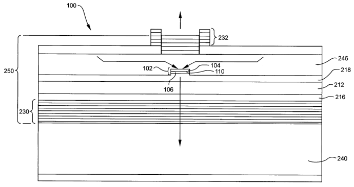
[0032] FIG. 1 is a schematic side view of a tunnel junction structure of one
embodiment of the
present invention;
[0033] FIG. 2 is a schematic side view of a vertical cavity surface emitting
laser, incorporating
the tunnel junction structure of FIG. 1, in one embodiment of the present
invention;
[0034] FIG. 3A is a graph of absorption vs energy for a bulk p-doped AlGaAsSb
layer 106 on an
InP substrate 240 of FIG. 2, according to the present invention;
[0035] FIG. 3B is a graph of photoluminescence (PL) intensity vs energy for a
bulk p-doped
AlGaAsSb layer 106 on an InP substrate 240 of FIG. 2, according to the present
invention;
[0036] FIG. 4A is a graph of the absorption vs energy in a p-doped GaAs layer;
and
[0037] FIG. 4B is a graph of the absorption vs energy in an n-doped GaAs
layer.
DETAILED DESCRIPTION OF THE PREFERRED EMBODIMENTS
[0038] Reference will now be made in detail to the present preferred
embodiments of the
invention, examples of which are illustrated in the accompanying drawings.
Whenever possible,
the same reference numerals will be used throughout the drawings to refer to
the same or like
parts. One embodiment of a semiconductor device of the present invention is
shown in FIG. 1,
and is designated generally throughout by the reference numeral 100.
[0039] Referring to FIG. 1, a tunnel junction device 102 with minimal hydrogen
passivation of
acceptors includes a p-type tunnel junction layer 106 of a first semiconductor
material doped
with carbon (C). As part of a new material systems combination, the first
semiconductor
material includes alurninum (Al), gallium (Ga), arsenic (As) and antimony
(Sb). The present
invention uses carbon doped AlGaAsSb as the p-material for the tunnel junction
because
hydrogen compensation of carbon acceptors is significantly less than in
materials such as
AlGaInAs, which has been previously used for forming the p-type tunnel
junction layer.
[0040] Juxtaposed with the p-type tunnel junction layer 106, an n-type tunnel
junction layer 104
of a second semiconductor material includes indium (In), gallium (Ga), arsenic
(As) and one of
aluminum (Al) and phosphorous (P). The junction between the p-type and an-type
tunnel
junction layers forms a tunnel junction 110.
8
CA 02567028 2006-11-16
WO 2005/117135 PCT/US2005/017288
[0041] At least one of the tunnel junction layers 104 or 106 has a thickness
<_ 30nm. Preferably,
each of the tunnel junction layers 104 and 106 has a thickness < 30nm.
[0042] Referring to FIG. 2, the semiconductor device 100 of FIG. 1 is shown
with more detail as
a light-emitting device, with the tunnel junction structure 102 of FIG. 1
incorporated. An InP
substrate 240 has an upper side and a lower side opposite the upper side, and
being characterized
by a substrate bandgap and a substrate lattice constant. Because the tunnel
layers 104 and 106
are grown sufficiently thin, at least one of the tunnel layers can have a
strain matched within +/-
2% of the substrate lattice constant.
[0043] It will be appreciated that the InP substrate 240, can optionally be
removed, after crystal
growth. However, because the InP substrate is needed for crystal growth, the
tunnel junction still
needs to satisfy the lattice match condition. A first interference reflector
230, such as a
distributed Bragg reflector (DBR) consisting of a GaAs/AlAs mirror, can be
deposited or bonded
to the InP based tunnel junction 102 and an active region 212 after removal of
the InP substrate
240.
[0044] The active region 212 is grown over the upper side of the InP substrate
240. The active
region 212 has an effective bandgap configured to generate light at a lasing
wavelength in
response to injected charge from the tunnel junction structure 102. By design,
the active region
212 is structured to generate light having a wavelength between 1000 nm and
1650 nm.
[0045] The first interference reflector 230, which strongly reflects light at
the lasing wavelength,
is disposed near the InP substrate 240 and remote from the tunnel junction
structure 102. A
second interference reflector 232 is disposed remote from the first
interference reflector 230 and
near the tunnel junction structure 102. The second interference reflector 232
substantially
reflects light at the lasing wavelength generated by the active region 212
disposed between the
first and second interference reflectors 230 and 232.
[0046] An optical distance between the opposed ends of the first and second
interference
reflectors 230 and 232 being in a predetermined relationship with the lasing
wavelength forms a
vertical optical cavity 250 for a vertical cavity surface emitting laser
(VCSEL). To provide the
required optical distance, one or more spacers are disposed between the first
and second
interference reflectors 230 and 232. For example, a substrate-side spacer
layer 216 and a
remote-side spacer layer 218 sandwiches the active region 212 while a tunnel
junction spacer
9
CA 02567028 2006-11-16
WO 2005/117135 PCT/US2005/017288
layer 246 surrounds the tunnel junction structure 102. By design, the optical
cavity 250 is now
resonant at the lasing wavelength of the light generated in the active region
212.
[0047] Preferably, the tunnel junction structure 102 is epitaxially grown in
an OMCVD chamber
with a temperature setting in a range about 400-700 degree C. Epitaxially
grown between the n-
type tunnel junction layer 104 and the active region 212, the first
semiconductor material of the
first tunnel junction layer is doped with a carbon concentration in a range
from about 1.5 x 10¹⁹
cm"3 to 3 x 1020cm "3 to form the p-type tunnel junction layer 106.
[0048] Similarly grown, the second semiconductor material is doped with a
silicon (Si)
concentration in a range from about 1.5 x 1019 cm"3 to 5 x 1019cm "3 to
provide an n- type tunnel
junction layer 104. However, other n-type dopants, such as Sn, can be used.
100491 Referring to FIGS. 3A and 3B, the graphs of absorption vs energy and
photoluminescence (PL) intensity vs energy are shown respectively, for a bulk
p-doped
AlGaAsSb layer 106 on an InP substrate 240 of FIG. 2. In accordance with the
invention, the p-
type tunnel junction layer 104 is designed to have an effective bandgap 414
greater than the
energy of the lasing wavelength at room temperature 312 by at least 80 milli
electron Volts
(meV).
[0050] The energy at which the PL peak occurs corresponds approximately to the
effective
bandgap 414of the material. As can be seen from FIG. 3A, the absorption at
this energy is high.
From FIG. 3A, it can be seen that the absorption decreases by about two orders
of magnitude at
an energy which is 80 meV below the PL peak energy. In order to minimize the
absorption of
the laser light, one needs to choose the composition of the p-doped AlGaAsSb
layer 106 to be
such that the PL peak energy of this material (which is roughly the effective
bandgap energy) to
be 80 meV above the photon energy of the lasing wavelength 312. This 80meV
separation is
needed between the effective bandgap 414 of the tunnel junction layers and the
photon energy of
the lasing wavelength 312, and not between the intrinsic bandgap of the tunnel
junction layers
and photon energy of the lasing wavelength. Deterniining the optimum bandgap
value, ahead of
time saves fabrication resources and time. Hence, the effective bandgap of the
carbon doped
AlGaAsSb p-tunnel junction layer 106 (and the n-doped tunnel junction layer
104) should each
satisfy the following equation where the effective bandgap 414 is related to
the photon energy of
the lasing wavelength 312:
CA 02567028 2006-11-16
WO 2005/117135 PCT/US2005/017288
Effective Bandgap(meV)_Energy of Lasing wavelength at room
temperature(meV)+80meV
(Eq. 1)
[0051] Using Eq. 1, the effective bandgap 414 of the n-type tunnel junction
layer is also related
to the photon energy of the lasing wavelength 312. In accordance with the
teachings of the
present invention, it is actually better to use the same equation for the n-
type layer as for the p-
type layer. This allows one to use a material with a smaller intrinsic
bandgap, which would be
better for increasing the probability of tunneling to enhance tunnel junction
performance. In the
case of n-type layers, the effective bandgap is larger than the intrinsic
bandgap, as can be seen in
FIG. 4B.
[0052] Referring to FIGS. 4A and 4B, the absorption vs energy in p- and n-
doped GaAs are
graphed, respectively. Graphs for AlGaAsSb p-type tunnel junction layer 106
and AlGaInAs n-
type tunnel junction layer would be similar except that the curves would be
shifted to lower
energy values. Even though GaAs is shown instead of A]GaAsSb the same tendency
between
the curves for the p-layer and n-layer is present.
[0053] The progression of the curves numbering increases as the dopant
concentration increases.
For example curve 400 represents the case for a high purity GaAs sample as the
starting
reference in both the p-type doping graph of FIG. 4A where the free hole
concentration is about
1.6x 1016cm crrfthe n-type doping graph of 4B where the free electron
concentration is about
5x 1013cm 3. Increasing in dopant concentrations, curves 422, respectively,
represent the next
higher concentration in both the p-type doping graph of FIG. 4A, where the
free hole
concentration is about 2.2x 10¹⁷crri 3, and the n-doping graph of 4B, where
the free electron
concentration is about 5.9x 101 1cm 3. The progression of curves continue in a
similar series with
the next curves 424, 426, 428, and 430 (only seen in FIG. 4A).
(0054] From comparing the graphs, the absorption edge 402 of the p-type layer
tends to shift to
smaller energies as the p-dopant concentration increases, as seen in the
progression of the curves
numbering increasing as the dopant concentration increases.
[0055] On the other hand, the absorption edge 402 of the n-type layer shifts
to higher energies as
seen in the progression of the curves numbering increasing as the dopant
concentration increases.
Thus, the effective bandgap 414 is seen to be larger than the intrinsic
bandgap 412 due to the
Moss-Burstein effect in n-type semiconductors. Thus, it is not a problem to
design the bandgap
11
CA 02567028 2006-11-16
WO 2005/117135 PCT/US2005/017288
of n-type tunnel junction layer 104 using the value of the intrinsic bandgap
which is described in
the Agilent patent application US2004/005 1 1 1 3.
[0056] In paragraph 52 of the Agilent patent application US2004/005 1 1 1 3,
the intrinsic bandgap
of the n-type layer is taught to be different from the p-type material which
has a sufficiently high
intrinsic bandgap to avoid absorption of the light generated in the active
region. The bandgap of
each n and p layer should be as low as possible to increase the probability of
tunneling and make
a better tunnel junction. Furthermore, the Agilent patent application
US2004/005 1 1 1 3 teaches
that the energy difference between the valence band energy of the material of
the p-type tunnel
junction layer and the conduction band energy of the material of the n-type
tunnel junction layer
should also be small.
[0057] If the n-type layer which has the same intrinsic bandgap as the photon
energy of lasing
wavelength is used, the effective bandgap 414 of this layer (which is much
higher than the
intrinsic bandgap 412) most likely already satisfies Eq. 1. Other companies
have already
demonstrated a VCSEL with a tunnel junction which has a narrower intrinsic
bandgap n-type
layer than the photon energy of the lasing wavelength.
[0058] However, the p-type junction layer 106 has a problem, if designed
according to the
Agilent patent application US2004/0051113. That is why an 80 meV separation
between the
effective bandgap and the photon energy of the lasing wavelength is suggested
for p-type
materials. In accordance with teachings of the present invention, the doping
of the first
semiconductor material having an intrinsic bandgap to form the p- type tunnel
junction layer
with the carbon concentration is so high that undesirable bandtails are formed
which in effect
decreases the intrinsic bandgap 412 of the p-type layer to the effective
bandgap 414.
[0059] The bandtails (causing the effects 404) effectively decrease the
bandgap 414 of the p-type
layer from its undoped or intrinsic value 412 - that is why it has an
effective bandgap 414, which
is different from the real (or intrinsic) bandgap 412. A larger intrinsic
bandgap is needed as the
doping increases in the p-type layer because the bandtail (causing the effects
404) increases and
reduces the effective bandgap 414.
[0060] Absorption by the tunnel junction layers 104 and 106 is further
minimized by placing
them at a null in the standing wave pattern formed by the laser light within
the VCSEL.
12
CA 02567028 2006-11-16
WO 2005/117135 PCT/US2005/017288
[0061] An aluminum fraction significantly greater than that at which light
absorption is
prevented should be avoided to maintain the desirable small difference between
the valence band
energy of the material of the p-type tunnel junction layer and the conduction
band energy of the
material of the n-type tunnel junction layer, and also to maintain as small a
bandgap as possible.
[0062] According to the teachings of the present invention, the bandgap is
varied independent of
the strain to offer more flexibility to overcome the undesired absorption in
the tunnel junction
layers. The strain and bandgap can be decoupled, according to the teachings of
the present
invention. The reason the first semiconductor material includes aluminum (Al)
in the p-type
tunnel junction layer is for decoupling the lattice strain from the bandgap by
maintaining the
lattice constant of the p-type tunnel junction layer 106 and allowing the
effective bandgap of the
p-type tunnel junction layer 106 of the tunnel junction structure 102 to be
higher than the photon
energy of the lasing wavelength to avoid absorption.
[0063] Including Al in the p-type tunnel junction layer does not influence the
n-type layer of the
tunnel junction. Also, including the Al maintains the lattice constant of the
p-type tunnel
junction layer and allows one to adjust the strain in the p-type tunnel
junction layer while
maintaining the bandgap. The strain can be up to 2% in the 30 nm p-tunnel
junction layer
(similarly for the n-tunnel junction layer) without introducing dislocations
in the strained layer.
[0064] By adding Al, the same lattice constant can be maintained, but the
bandgap can increase.
When one changes the As/Sb ratio in GaAsSb the bandgap changes and since the
lattice constant
changes, so does the strain. When one changes the Al/Ga ratio in AlGaAsSb (or
in AlGaInAs,
AlGaAs, etc) the lattice constant is nearly constant, only the bandgap
changes.
[0065] In accordance with the invention, the wavelength at which absorption
occurs in the p-type
AlGaAsSb layer is thus decreased in order to compensate for the effect of the
undesirable
bandtails. The decreasing step includes adjusting the composition of the p-
type AlGaAsSb layer
by suitably adjusting the Al/Ga and As/Sb ratios in order to obtain a low
enough absorption such
that the p-type AlGaAsSb layer has the effective bandgap greater than the
photon energy of the
lasing wavelength at room temperature by at least 80 milli electron Volts.
Only the Al/Ga ratio
is adjusted if the strain is to be kept constant.
[0066] Experimentally, one adjusts the As/Sb ratio at a given doping level to
control the strain
and the Al/Ga ratio to control the effective bandgap (80 meV above or equal to
the photon
13
CA 02567028 2006-11-16
WO 2005/117135 PCT/US2005/017288
energy of the lasing wavelength). Calculations of the strain change seem to
suggest that the
strain change with doping up to 5 x 1019 cm"3 is very small and can be
neglected. In any case,
the introduction of the dopant gas (CBr4 or CC14) changes the growth chemistry
and introduces
a change in the As/Sb ratio (and possibly Al/Ga ratio), which changes the
strain, and because the
effective bandgap changes with doping, it is difficult to detemline what the
composition of the
AlGaAsSb is but it can be adjusted to obtain the desired effective bandgap and
strain.
[0067] In order to maintain the strain between In,,GayAl({_X_y)As and InP at
+/-2%, x should
satisfy 0.83_x>0.24, with the value of y adjusted to achieve the desired
bandgap.
The semiconductor material of the n-type tunnel junction layer 104 consists
essentially of Indium
Gallium Aluminum Arsenide (InGayAl(l_,,_y)As), in which 0.83~!X>-0.24 and y>0,
according to
the teachings of the present invention for the optimum selection of material
systems. With such
a material composition for the n-type tunnel junction layer 104, the
semiconductor material of
the p-type tunnel junction layer 106 consists essentially of aluminum gallium
arsenide
antimonide A1YGa(,_Y)As(,_,,)Sb,,, in which 0.752>x>0.22, and y _0.
[0068] Alternatively, regardless of the composition of the n-type tunnel
junction layer 104, the
semiconductor material of the p-type tunnel junction layer consists
essentially of aluminum
gallium arsenide antimonide AIyGa(,_y)As(i_,,)Sb,,, in which 0.752>x>0.22, and
y>0.
[0069] If the semiconductor material of the n-type tunnel junction layer 104
consists essentially
of Indium Gallium Arsenide Phosphide InyGa(t_y)As(l_,,)P,, in which 1>x->0 and
1> y> 0.24, then
the semiconductor material of the p-type tunnel junction layer consisting
essentially of aluminum
gallium arsenide antimonide AlyGa(t_Y)As(I_,,)Sb,,, in which 0.752>x>0.22, and
y>0 will be used
as the carbon doped p-type material for the tunnel junction.
[0070] If the InYGa(,_y)As(l_X)PX is lattice matched to InP then
y=(0.2154+0.2021 x)/(0.4051+0.0125x) (Eq. 2.)
However, the InYGa(,_y)As(,_X)PX layer can be designed to have a strain of+/-
2%.
AlGaAsSb is the preferred p-type tunnel junction layer, since we have found
that hydrogen
compensation of carbon acceptors is significantly less than in materials such
as AlGaInAs, which
is commonly used for forming the tunnel junction.
14
CA 02567028 2006-11-16
WO 2005/117135 PCT/US2005/017288
EXAMPLE
[0071] The invention will be further clarified by the following example.
EXAMPLE 1
[00721 The band gap of the p-type AlGaAsSb tunnel junction layer 106 can thus
be adjusted to a
suitable value by adjusting the Al/Ga ratio. The p-type AlGaAsSb layer 106 and
the A]GaInAs.
layer 1041ayers may be strained. For 1.3 micron VCSELs the effective bandgap
wavelengths of
AlGaAsSb and AlGaInAs are selected to be 1.2 microns but other suitable values
may also be
used, as long as Eq. 1 is satisfied. C-doped AlGaAsSb is grown by OMCVD using
suitable
precursors such as trimethylaluminum, triethylgallium, arsine,
trimethylantimony and carbon
tetrabromide. However, any other growth method could be used. Hole
concentrations of
-3 x 1020 cm"3 have been achieved in AlGaAsSb. The carrier gas was hydrogen
and the growth
temperature was -550 C. A higher growth temperature is preferred in order to
minimize
hydrogen compensation of the C acceptors. The reagents were trimethylaluminum,
triethylgallium, trimethylindium, arsine, phosphine, trimethylantimony,
disilane and carbon
tetrabromide. The reagent flows were adjusted to achieve an effective bandgap
wavelength of
1.2 microns for both AIGaAsSb and AlGaInAs, while achieving lattice matching
to an InP
substrate. The p-doping was done using carbon tetrabromide. The n-doping was
done using
disilane.
[0073] It will be apparent to those slcilled in the art that various
modifications and variations can
be made to the present invention without departing from the spirit and scope
of the invention.
Thus it is intended that the present invention cover the modifications and
variations of this
invention provided they come within the scope of the appended claims and their
equivalents.