Note: Descriptions are shown in the official language in which they were submitted.
CA 02567523 2006-11-21
WO 2005/122377 PCT/US2005/018794
INTEGRATION OF PLANAR TRANSFORMER AND/OR PLANAR INDUCTOR
WITH POWER SWITCHES IN POWER CONVERTER
BACKGROUND OF THE INVENTION
Field of the Invention
This disclosure generally relates to electrical power systems, and
more particularly to power module architectures suitable for rectifying,
inverting,
and/or converting electrical power between power sources and loads.
Description of the Related Art
Power modules are typically self-contained units that transform
and/or condition power from one or more power sources for supplying power to
one or more loads. Power modules commonly referred to as "inverters"
transform direct current (DC) to alternating current (AC), for use in
supplying
power to an AC load. Power modules commonly referred to as "rectifiers"
transform AC to DC. Power modules commonly referred to as "DC/DC
converters" step up or step down a DC voltage. An appropriately configured
and operated power module may perform any one or more of these functions.
The term "converter" commonly applies generically to all power modules
whether inverters, rectifiers and/or DC/DC converters, and is used herein in
that
generic sense.
Many applications employ the delivery of high power, high current
and/or high voltage from a power source to a load. For example, transportation
applications may employ high power to drive a load such as a traction motor
for
propelling an electric or hybrid electric vehicle. Such applications may
employ
one or more of a variety of power sources, for example, energy producing
power sources such as arrays of fuel cells or photovoltaic cells, and/or
energy
storage power sources such as arrays of battery cells and/or super capacitors.
Often, such applications employ a power converter to transform and/or
1
CA 02567523 2006-11-21
WO 2005/122377 PCT/US2005/018794
condition the power, for example, stepping down the voltage at which the power
is supplied to the load.
Power converters typically employ power semiconductor devices,
such as insulated gate bipolar transistors (IGBTs), metal oxide semiconductor
field effect transistors (MOSFETs), and/or semiconductor diodes. These power
semiconductor devices dissipate large amounts of heat during high power
operation, creating thermal management problems which may limit the
operating range, increase cost, increase size and/or weight, adversely effect
efficiency, and/or reduce reliability of the power converter.
Methods and, or architectures for power converters capable of
high power operation that alleviate the thermal management problems are
highly desirable.
BRIEF SUMMARY OF THE INVENTION
In one aspect, a power converter comprises a heat sink; a
magnetic core capable of producing a magnetic field; at least a first multi-
layer
substrate comprising at least two electrically and thermally conductive
layers,
and at least one electrically insulative and thermally conductive layer, each
of
the electrically and thermally conductive layers of the first multi-layer
substrate
electrically isolated from a next successive one of the electrically and
thermally
conductive layers by a respective one of the electrically insulative and
thermally
conductive layers, at least a first one of the electrically and thermally
conductive
layers patterned to form a first winding, at least a second one of the
electrically
and thermally conductive layers patterned to form a second winding, at least a
portion of each of the first and the second windings disposed within the
magnetic field of the magnetic core to form a planar transformer, the first
multi-
layer substrate thermally coupled to the heat sink; and at least a first power
semiconductor device electrically coupled to one of the electrically and
thermally conductive layers of the first multi-layer substrate, the first
power
semiconductor device electrically isolated from and thermally coupled to the
heat sink via the first multi-layer substrate.
2
CA 02567523 2006-11-21
WO 2005/122377 PCT/US2005/018794
In another aspect, a power converter comprises a heat sink; a first
multi-layer substrate comprising at least two electrically and thermally
conductive layers, and at least one electrically insulative and thermally
conductive layer, each of the electrically and thermally conductive layers of
the
first multi-layer substrate electrically isolated from a next successive one
of the
electrically and thermally conductive layers by a respective one of the
electrically insulative and thermally conductive layers; at least a first
power
semiconductor device electrically coupled to a portion of an outermost one of
the electrically and thermally conductive layers of the first multi-layer
substrate,
the first power semiconductor device electrically isolated from and thermally
coupled to the heat sink via the first multi-layer substrate; a magnetic core
capable of producing a magnetic field; and at least a second multi-layer
substrate comprising at least two electrically and thermally conductive
layers,
and at least one electrically insulative and thermally conductive layer, each
of
the electrically and thermally conductive layers of the second multi-layer
substrate electrically isolated from a next successive one of the electrically
and
thermally conductive layers by a respective one of the electrically insulative
and
thermally conductive layers, at least a first one of the electrically and
thermally
conductive layers patterned to form a first winding, at least a second one of
the
electrically and thermally conductive layers patterned to form a second
winding,
at least a portion bf each of the first and the second windings disposed
within
the magnetic field of the magnetic core to form a planar transformer, the
second
multi-layer substrate thermally coupled to the heat sink.
In still another aspect, a power converter comprises a heat sink; a
first multi-layer substrate comprising at least a first layer, a second layer,
and
third layer, the first layer comprising an electrically and thermally
conductive
material patterned to from a first inductor, the second layer comprising an
electrically insulative and thermally conductive material, and the third layer
comprising an electrically and thermally conductive material, the second layer
electrically isolating the third layer from the first layer, the third layer
of the first
multi-layer substrate thermally conductively coupled to the heat sink; at
least a
3
CA 02567523 2006-11-21
WO 2005/122377 PCT/US2005/018794
first power semiconductor device thermally coupled to a first portion of the
first
layer; a magnetic core with a magnetic field; and at least a second multi-
layer
substrate comprising at least a first layer, a second layer, and a third
layer, the
first layer comprising an electrically and thermally conductive material, the
second layer comprising an electrically insulative and thermally conductive
material, the third layer comprising an electrically and thermally conductive
material, the second layer electrically isolating the third layer from the
first layer,
the third layer patterned to form a first winding, the first layer patterned
to form
a second winding, at least a portion of the first and the second conductive
layers disposed within the magnetic field of the magnetic core to form a
planar
transformer, the second multi-layer substrate thermally conductively coupled
to
the heat sink.
In yet another aspect, a power converter comprises: at least a first
heat sink; at least a first magnetic core capable of producing a magnetic
field; at
least a first multi-layer substrate comprising at least two electrically and
thermally conductive layers, and at least one electrically insulative and
thermally conductive layer, each of the electrically and thermally conductive
layers of the first multi-layer substrate electrically isolated from a next
successive one of the eiectrically and thermally conductive layers by a
respective one of the electrically insulative and thermally conductive layers,
at
least a first one of the electrically and thermally conductive layers
patterned to
form a first winding of at least a first planar transformer and a first
winding of a
first inductor, at least a second one of the electrically and thermally
conductive
layers patterned to form a second winding of the first planar transformer, at
least a portion of each of the first and the second winding of the planar
transformer disposed within the magnetic field of the magnetic core, the first
multi-layer substrate thermally coupled to the heat sink; and at least a first
power semiconductor device electrically coupled to one of the electrically and
thermally conductive layers of the first multi-layer substrate, the first
power
semiconductor device electrically isolated from and thermally coupled to the
heat sink via the first multi-layer substrate.
4
CA 02567523 2006-11-21
WO 2005/122377 PCT/US2005/018794
In a further aspect, a method of forming a power converter
comprises providing a heat sink, providing a number of multi-layer switch
substrates, each of the multi-layer switch substrates comprising at least two
electrically and thermally conductive layers, and at least one electrically
insulative and thermally conductive layer, each of the electrically and
thermally
conductive layers of the multi-layer switch substrate isolated from a next
successive one of the electrically and thermally conductive layers by a
respective one of the electrically insulative and thermally conductive layers;
for
each of the multi-layer switch substrates, soldering at least one respective
power semiconductor device to one of the electrically and thermally conductive
layers of the multi-layer switch substrate; for each of the multi-layer switch
substrates, soldering one of the electrically insulative and thermally
conductive
layers of the multi-layer switch substrate to the heat sinks; providing a
magnetic
core; providing a multi-layer transformer substrate comprising at least two
electrically and thermally conductive layers, and at least one electrically
insulative and thermally conductive layers, each of the electrically and
thermally
conductive layers of the multi-layer transformer substrate isolated from a
next
successive one of the electrically and thermally conductive layers by a
respective one of the electrically insulative and thermally conductive layers;
patterning at least one of the electrically and thermally conductive layers of
the
multi-layer transformer substrate to form a first winding; patterning at least
one
of the electrically and thermally conductive layers of the multi-layer
transformer
substrate to form respective portions of a second winding; disposing at least
a
portion of each of the first and the second windings within the magnetic field
of
the magnetic core to form a planar transformer; and soldering one of the
electrically insulative and thermally conductive layers of the multi-layer
transformer substrate to the heat sink.
BRIEF DESCRIPTION OF THE SEVERAL VIEWS OF THE DRAWING(S)
In the drawings, identical reference numbers identify similar
elements or acts. The sizes and relative positions of elements in the drawings
5
CA 02567523 2006-11-21
WO 2005/122377 PCT/US2005/018794
are not necessarily drawn to scale. For example, the shapes of various
elements and angles are not drawn to scale, and some of these elements are
arbitrarily enlarged and positioned to improve drawing legibility. Further,
the
particular shapes of the elements as drawn, are not intended to convey any
inforrnation regarding the actual shape of the particular elements, and have
been solely selected for ease of recognition in the drawings.
Figure 1 is an electrical schematic of a power converter according
to one illustrated embodiment.
Figure 2A is a top front left isometric view of a portion of the
power converter of Figure 1, with a cover removed from a module housing to
show an inverter, a rectifier, two planar transformers, filter inductors, and
an
integrated base plate heat sink.
Figure 2B is a top front left isometric view of a portion of an
integrated base plate heat sink showing a number of multi-layer switch
substrates physically and thermally coupling respective switches of the
rectifier
to the integrated base plate heat sink according to one illustrated
embodiment.
Figure 2C is a top front left isometric view of a portion of an
integrated base plate heat sink showing two multi-layer switch substrates each
comprising two distinct areas formed in an electrically and thermally coupled
layer to physically and thermally couple respective switches of the rectifier
to
the integrated base plate heat sink, according to another illustrated
embodiment.
Figure 2D is a top front left isometric view of a portion of an
integrated base plate heat sink showing a single multi-layer switch substrate
comprising four distinct areas formed in an electrically and thermally coupled
layer to physically and thermally couple respective switches of the rectifier
to
the integrated base plate heat sink, according to another illustrated
embodiment.
Figure 3 is a top front left isometric view of one of the planar
transformers, according to one illustrated embodiment.
6
CA 02567523 2006-11-21
WO 2005/122377 PCT/US2005/018794
Figure 4 is an exploded top left front isometric view of the planar
transformer of Figure 3.
Figure 5 is a top front left isometric view of one of the planar
inductor, according to one illustrated embodiment.
Figure 6 is an exploded top left front isometric view of the planar
inductor of Figure 5.
Figure 7A is a top left front isometric view of a power converter
according to another illustrated embodiment, in which the inverter and filter
inductors are in the module housing.
Figure 7B is a top front left isometric view of a portion of an
integrated base plate heat sink showing a single multi-layer switch substrate
comprising ten distinct areas formed in an electrically and thermally coupled
layer to physically and. thermally couple respective switches of the rectifier
and
inverter to the integrated base plate heat sink, according to another
illustrated
embodiment.
Figure 7C is a top front left isometric view of a portion of an
integrated base plate heat sink showing a single multi-layer substrate
comprising ten distinct areas formed in an electrically and thermally coupled
layer to physically and thermally couple respective switches of the rectifier
and
inverter to the integrated base plate heat sink, as well as area for forming
the
windings of the two transformers, according to another illustrated embodiment.
Figure 7D is a top front left isometric view of a portion of an
integrated base plate heat sink similar to that of Figure 7C, showing the use
of
one of the electrically and thermally conductive layers of the multi-layer
substrate electrically coupling the second side of the transformers to
respective
terminals of the power semiconductor switches of the rectifier.
Figure 7E is a top front left isometric view of a portion of an
integrated base plate heat sink similar to that of Figure 7D, showing the use
of
one of the electrically and thermally conductive layers of the multi-layer
substrate electrically coupiing the second side of the transformers to
respective
7
CA 02567523 2006-11-21
WO 2005/122377 PCT/US2005/018794
terminals of the power semiconductor switches of the rectifier and to planar
inductors.
Figure 8 is a top front left isometric view of the integrated base
plate heat sink according to one illustrated embodiment.
Figure 9 is a graph illustrating control signals for controlling
operation of the power converter, as well as resulting voltage and current
plots,
according to one illustrated embodiment.
DETAILED DESCRIPTION OF THE INVENTION
In the following description, certain specific details are set forth in
order to provide a thorough understanding of various embodiments. However,
one skilled in the art will understand that the invention may be practiced
without
these details. In other instances, well-known structures associated with power
converters, controllers and/or gate drives have not been shown or described in
detail to avoid unnecessarily obscuring descriptions of the embodiments.
Unless the context requires otherwise, throughout the
specification and claims which follow, the word "comprise" and variations
thereof, such as, "comprises" and "comprising" are to be construed in an open
sense, that is as "inciuding, but not limited to."
Reference throughout this specification to "one embodiment" or
"an embodiment" means that a particular feature, structure or characteristic
described in connection with the embodiment is included in at least one
embodiment. Thus, the appearances of the phrases "in one embodiment" or "in
an embodiment" in various places throughout this specification are not
necessarily all referring to the same embodiment. Further more, the particular
features, structures, or characteristics may be combined in any suitable
manner
in one or more embodiments.
The headings provided herein are for convenience only and do
not interpret the scope or meaning of the claimed invention.
Figure 1 shows a power converter 10, according to one illustrated
embodiment in which the power converter 10 takes the form of a DC/DC power
8
CA 02567523 2006-11-21
WO 2005/122377 PCT/US2005/018794
converter. The power converter 10 is operable to transform and/or condition
power supplied by a power source VI for supply to one or more loads R1, R2.
The power converter 10 may comprise an inverter 12, a rectifier 14, and a pair
of transformers T1, T2 galvanically coupling the inverter 12 with the
rectifier 14.
The power converter 10 may also comprise a pair terminals 16a, 16b, which
may be electrically coupled to receive power from the power source VI. The
power source VI may, for exampie, take the form one or more energy producing
power sources such as arrays of fuel cells or photovoltaic cells, and/or may
take the form of one or more energy storage power sources such as arrays of
battery cells and/or super capacitors. The power converter 10 also comprises a
set of terminals 18a, 18b, 18c, which may be electrically coupled to supply
power to one or more loads RI, R2.
The inverter 12 comprises an inverter side bus 20 (collectively)
formed by voltage rails 20a, 20b. The inverter 12 also comprises a first phase
leg 12a formed by an upper power semiconductor switch S1 and lower power
semiconductor switch S2, a second phase leg 12b formed by an upper power
semiconductor switch S3 and lower power semiconductor switch S4, and a third
phase leg 12c formed by an upper power semiconductor switch S5 and lower
power semiconductor switch S6, each of the phase legs 12a-12c electrically
coupled between the voltage rails 20a, 20b. The power semiconductor
switches S1-S6 may, for example, take the form of metal oxide semiconductor
field effect transistors (MOSFETs), insulated gate bipolar transistors (IGBTs)
and/or other switches suitabie for high power operation.
The inverter 12 further comprises power semiconductor diodes
D1-D6, electrically coupled in anti-parallel across respective ones of the
power
semiconductor switches S1-S6. As used herein and in the claims, the term
"power semiconductor device" includes semiconductor devices designed to
handle large currents, large voltages and/or large amounts of power with
respect to standard semiconductor devices, including power semiconductor
switches devices, power semiconductor diodes, and other such devices used in
power distribution, for example, grid or transportation related applications.
In
9
CA 02567523 2006-11-21
WO 2005/122377 PCT/US2005/018794
some embodiments, the power semiconductor diodes D1-D6 may be formed as
part of the power semiconductor switches S1-S6, for example as body diodes,
while in other embodiments the power semiconductor diodes D1-D6 may take
the form of discrete semiconductor devices.
Between the pair of power semiconductor switches S1, S2, S3,
S4, S5, S6 forming each phase leg 12a, 12b, 12c respectively, is a phase node
A, B, C, upon which the respective phase of a three phase output of the
inverter
12 appears during operation. While illustrated as a single switch and diode,
each of the power semiconductor switches S1-S6 and/or diodes D1-D6 may
take the form of one or more power semiconductor switches and/or diodes
electrically coupled in parallel. A controller 24 controls the power
semiconductor switches S1-S6 via control signals 26.
The inverter 12 may further comprise an input capacitor Cl,
electrically coupled across the voltage rails 20a, 20b of the inverter side
bus 20.
The rectifier 14 may take the form of an active rectifier, such as
the current doubler rectifier illustrated in Figure 1. The rectifier 14
comprises a
first leg 14a formed by an upper power semiconductor switch S7 and lower
power semiconductor switch S9, and a second leg 14b formed by an upper
power semiconductor device switching S8 and lower power semiconductor
device switch S10. The rectifier 14 also comprises power semiconductor
diodes D7-D10, electrically coupled in anti-parallel across respective ones of
the power semiconductor switches S7-S10, respectively. In some
embodiments, the power semiconductor diodes D7-D10 may be formed as part
of the power semiconductor switches S7-S1 0, for example as body diodes,
while in other embodiments the power semiconductor diodes D7-D10 may take
the form of discrete semiconductor devices. While illustrated as a single
switch
and diode, each of the power semiconductor switches S7-S10 and/or diodes
D7-D10 may take the form of one or more power semiconductor switches
and/or diodes electrically coupled in parallel.
A node between each of the first and the second legs 14a, 14b of
the rectifier 14 are electrically coupled to one another to provide a neutral
node
CA 02567523 2006-11-21
WO 2005/122377 PCT/US2005/018794
0 for the rectifier 14. The controller 24 controls the power semiconductor
switches S7-S10 via control signals 28.
The transformers T1, T2 may be high frequency transformers,
which provide galvanic isolation, and voltage step up/step down between the
inverter side and the rectifier side of the power converter 10. Each
transformer
TI, T2 share half the power of the power converter 10.
The first transformer T1 comprises a first side T1 a and a second
side T1 b. Where power is transferred from the power source VI to the load(s)
RI, R2, the first side T1a is typically referred to as the primary winding and
the
second side T1 b as the secondary winding. In some embodiments, power may
transfer in the opposite direction, for example during regenerative braking
power may transfer from the "load(s)" R1, R2 (e.g., electric machine) to the
"power source" VI (e.g., battery and/or super-capacitor). Consequently, the
terms first and second side are used throughout this description and in the
claims to generically refer to the windings of the transformers Tl, T2 without
regard to the direction of power transfer. Likewise, as used throughout this
description and in the claims, the load(s) RI, R2 may consume power in a first
mode (e.g., driving), while generating power in a second mode (e.g.,
regenerative braking), and the power supply VI may provide power in the first
mode, while consuming or storing power in the second mode. Other modes
and operations are possible.
The first side T1 a of the first transformer TI includes a pair of
poles T1 c, T1 d, and the second side T1 b also includes a pair of poles T1 e,
T1f.
Likewise, the second transformer T2 comprises a first side T2a and a second
side T2b. The first side T2a of the second transformer T2 includes a pair of
poles T1 c, T1 d, and the second side T2b includes a pair of poles T2e, T2f.
The second side T2b of the second transformer T2 is electrically coupled to
respective current paths K, L, M, N that form a rectifier side bus which also
includes the neutral node 0 of the rectifier 14.
The phase node A of the first phase leg 12a of the inverter 12 is
electrically coupled to the first pole T1c of the first side T1a of the first
11
CA 02567523 2006-11-21
WO 2005/122377 PCT/US2005/018794
transformer T1. The phase node B of the second phase leg 12b of the inverter
12 is electrically coupled to the second pole T1d of the first side T1a of the
first
transformer TI, and coupled to the first pole T2c of the first side T2a of the
second transformer T2. The phase node C of the third phase leg 12c of the
inverter 12 is electrically coupled to the second pole T2d of the first side
T2a of
the second transformer T2.
The first leg 14a of the rectifier 14 is electrically coupled between
the first pole TI e of the second side TI b of the first transformer T1 via
current
path K and the second pole T2f of the second side T2b of the second
transformer T2 via current path N. The second leg 14b of the rectifier 14 is
electrically coupled between the second pole T1 f of the second side T1 b of
this
first transformer T1 via current path L and the first pole T2e of the second
side
T2b of the second transformer T2 via current path M. A filter inductor LI, L2,
L3, L4 is electrically coupled between each pole T1e, T1f, T2e, T2f of the
secondary sides T1 c, T2c of the transformers TI, T2 via the current paths K,
L,
M, N and the terminals 18a-18c. The filter inductors L1-L4 share the load
current. Output capacitors CO1, C02 are electrically coupled across each pair
of the terminals 18a-18b, 18b-18c.
The controller 24 provides control signals 26, 28 to control the
power semiconductor switches S1-6 of the inverter 12 and/or the power
semiconductor switches S7-S10 of the rectifier 14, respectively. The
controller
24 may take the form of a microcontroller such as a microprocessor, digital
signal processor (DSP) and/or application specific integrated circuit (ASIC).
Controller 24 may receive input signals such as voltage and current
measurements from a voltage sensor 40a and/or current sensor 40b that sense
voltage or current with respect to the input from the power source VI. The
controller 24 may additionally or alternatively receive voltage and/or current
signals from a voltage sensor 42a and/or current sensor 42b that measure
output voltage and/or current.
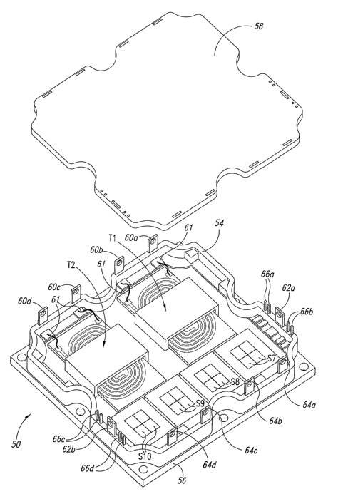
Figure 2A shows a power module 50 according to one illustrated
embodiment, the power module 50 housing a portion of the power converter 10
12
CA 02567523 2006-11-21
WO 2005/122377 PCT/US2005/018794
illustrated by broken line box 52 of Figure 1. In particular, the power module
50
comprises an electrically insulative lead frame 54, an integrated base plate
heat
sink 56 and an electrically insulative cover 58, collectively forming a
housing.
The Figure does not separately call out the power semiconductor diodes D6-
D10, which are formed as a part of the power semiconductor switches S6-S10
in this illustrated embodiment. As illustrated in Figure 2A, each of the power
semiconductor switches S6-S10 illustrated in Figure 1 may actually take the
form of one or more (four illustrated) power semiconductor switches S6-S10
electrically coupled in parallel with one another.
The lead frame 54 supports a number of external terminals or
connectors making electrical couplings external from the housing formed by the
lead frame 54, heat sink 56 and cover 58. For example, the power module 50
may include a number of terminals 60a-60d for making electrical couplings
between the phase nodes A, B, C of the inverter 12 and the poles of the first
sides T1a, T2a of the transformers T1, T2. In particular, a first terminal
60a,
electrically couples the phase node A of the inverter 12 to the first pole T1
c of
the transformer T1, via wire bonds 61. A second terminal 60b and a third
terminal 60c electrically couple the phase node B of the inverter 12 to the
second pole T1d of the first transformer T1 and the first pole T2c of the
second
transformer T2, respectively, via wire bonds 61. A fourth terminal 60d
electrically couples the phase node C of the inverter 12 to the second pole
T2d
of the second transformer T2 via wire bonds 61. While Figure 2A only
illustrates one wire bond 61 per electrical coupling, most practical
applications
with comprise a plurality of wire bonds for each electrical coupling:
Also for example, a number of terminals or connectors electrically
couple the rectifier 14 to the filter inductors L1-L4 and to the terminals 18a-
18c
via wire bonds (not shown). For example, a pair of terminals 62a, 62b
electrically couple the neutral node 0 of the rectifier 12 to the terminal
18b.
Other terminals 64a-64d electrically couple the rectifier 14 and/or second
sides
T1b, T2b of the transformers T1, T2 to the filter inductors L1-L2, via the
current
paths K-N.
13
CA 02567523 2006-11-21
WO 2005/122377 PCT/US2005/018794
Terminals or connectors such as pins 66a, 66b, 66c, 66d
electrically couple control signals 28 from the controller 24 to the power
semiconductor switches S7-S10 of the rectifier 14 via wire bonds (not shown).
The pins 66a-66d are located proximate the terminal 18b which is connected to
the neutral node O.
Many of the electrical couplings within the power module 50 are
advantageously made via wire bonds. For example, the electrical couplings
between the terminals 60a-60d and the first side T1 a, T2a of the transformers
T1, T2, are made via wire bonds 61. Also for example, the electrical couplings
between the second side TI b, T2b of the transformers T1, T2 and the power
semiconductor switches S7-S10 and power semiconductor diodes D7-D10 are
made via wire bonds (not shown). Further, the electrical couplings between
terminals 62a, 62b, 64a-64b and the power semiconductor switches S7-S10
and power semiconductor diodes D7-D1 0 are also made via wire bonds (not
shown).
Figures 2B-2D show how the power semiconductor switches S7-
S10 and power semiconductor diodes D7-D10 of the rectifier 14 are physically
mounted and thermally coupled to the integrated base plate heat sink 56 by one
or more multi-layer switch substrates 44, according to a number of illustrated
embodiments. The multi-layer switch substrates 44 comprise a first layer 44a
that is electrically and thermally conductive, a second layer 44b that is
electrically insulative and thermally conductive, and a third layer 44c that
is
electrically and thermally conductive. In some embodiments, the multi-layer
switch substrate 44 may comprise a greater number of layers.
In particular, Figure 2B shows one embodiment in which a
number of multi-layer switch substrates 44 are provided, one for each of the
power semiconductor devices S7-S10 and associated power semiconductor
diodes D7-D10 forming the rectifier 14. Thus, this embodiment of Figure 2B
may include a total of four separate multi-layer switch substrates 44 for the
rectifier 14.
14
CA 02567523 2006-11-21
WO 2005/122377 PCT/US2005/018794
Figure 2C shows another embodiment in which a number of muiti-
layer switch substrates 44 are provided, one for each leg 14a, 14b of the
rectifier 14. In such an embodiment, the eiectrically and thermally conductive
layer 44a of each of the multi-layer substrates 44 form distinct areas for
mounting each of the power semiconductor devices S7-S1 0 and associated
power semiconductor diodes D7-D1 0 forming the respective leg 14a, 14b of the
rectifier 14.
Figure 2D shows still a further embodiment in which a single
multi-layer switch substrate 44 is provided for forming entire the rectifier
14. A
number of distinct areas are formed in the first electrically and thermally
conductive layer 44a, the areas being electrically isolated from one another.
In
this embodiment, there is one area for each of the power semiconductor
devices S7-S10 and associated power semiconductor diodes D7-D10 forming
the rectifier 14, thus a total of four distinct areas.
Generally, the inclusion of fewer individual multi-layer substrates
44, 70 reduces the parts count, and may reduce the number of manufacturing
operations, although forming distinct areas may offset some of the savings in
manufacturing operations. However, such a reduction in number is typically
accompanied by an increase in size of the remaining multi-layer substrate(s)
44, 70. This increase in size increases the stresses to which the multi-layer
substrates 44, 70 are subject, and thus increases the likelihood of defects
occurring, such as cracks developing, for example, from solder reflow.
. Figures 3 and 4 show one of the transformers T1 in more detail.
The second transformer T2 may have a similar construction to that of the first
transformer TI.
The transformer TI comprises a multi-layer transformer substrate
70 and magnetic core 72. The multi-layer transformer substrate 70 includes a
first layer 70a that is electrically and thermally conductive, a second layer
70b
that is electrically insulative and thermally conductive, a third layer 70c
that is
electrically and thermally conductive, a fourth layer 70d that is electrically
insulative and thermally conductive, and a fifth layer 70f that is
electrically and
CA 02567523 2006-11-21
WO 2005/122377 PCT/US2005/018794
thermally conductive. The multi-layer transformer substrate 70 may include a
greater number of layers to vary the performance of the transformer T1, for
example, by varying the number of layers and hence the ratio of "turns"
between the primary and secondary windings of the transformer and/or by
reducing eddy currents.
The first layer 70a and fifth layer 70e are patterned to form
portions of a first winding, and electrically coupled through vias 74a, 74b
and
connecting pads 74c, 74d, 74e to form the first winding. The third layer 70c
is
also patterned to form a second winding. While the Figures illustrate the
first
winding comprising more layers than the second winding, in some
embodiments the second winding may comprises more layers than the first
winding, or may the first and second windings may comprises the same number
of layers.
The fifth layer 70e may be further patterned to form mounting
areas 70f for attaching the multi-layer transformer substrate 70 to the heat
sink
56, for example by soldering. This reduces the coupling area between the
multi-layer substrate 70 and the integrated base plate heat sink 56 reducing
associated stresses and the likelihood of imperfections developing such as
cracking, for example, during solder reflow.
The magnetic core 72 may include two or more portions 72a, 72b
that wrap around the first and second windings of the multi-layer transformer
substrate 70. A portion 72c of the magnetic core 72 may be received through
an opening 70g formed in each of the layers 70a-70e of the multi-layer
transformer substrate 70.
The multi-layer transformer substrate 70 may be formed using a
variety of techniques and materials, for example, the multi-layer substrates
70
may take the form of direct bonded copper (DBC) substrates available, for
example, from Curamik Electronics of Addison, Texas. Additionally or
alternatively, the multi-layer substrates 70 may take the form of insulated
metal
substrates (IMS) available, for example, from Bergquist Company of
Chanhassen, Minnesota.
16
CA 02567523 2006-11-21
WO 2005/122377 PCT/US2005/018794
The electrically and thermally conductive layers may take a
variety of forms such as copper, aluminum and/or other good electrical and
thermal conductors. While typically provided in the form of a film, the
electrically and thermally conductive layers may take other forms, for
example,
stamped sheet metal. The electrically insulative and thermally conductive
layers may, for example, take the form of a thermally enhanced polyimide film
such as Kapton film, available from Du Pont de Nemours, High Performance
Materials of Circleville, Ohio. Additionally, or alternatively, the
electrically
insulative and thermally conductive layers may, for example, take the from of
a
suitable ceramic, such as an alumina, aluminum nitride and/or silicon nitride
ceramic. ln one embodiment, the multi-layer transformer substrate 70 takes the
form of layers of stamped sheet metal that are laminated together with
insulative layers such as Mylar film, available from Du Pont de Nemours,
High Performance Materials of Circleville, Ohio, using an adhesive such as an
epoxy based adhesive.
The multi-layer switch and transformer substrates 44, 70 may be
attached to the integrated base plate heat sink 56 via solder reflow
techniques.
For example, the.power semiconductor switches S1-S10 and power
semiconductor diodes D1-D10 may be soldered onto respective multi-layer
substrates 44, 70, which are then positioned on the integrated base plate heat
sink 56. The multi-layer substrates 44, 70 are then soldered to the integrated
base plate heat sink 56 at a same time and/or in a single act, for example,
via
heating in an oven using solder reflow techniques.
Alternatively, the multi-layer substrates 44, 70 may be positioned
on the integrated base plate heat sink 56, the power semiconductor switches
S1-S10 and power semiconductor diodes D1-D10 may be positioned on the
multi-layer substrates 44, 70. The connections between the power
semiconductor switches S1-S10 and power semiconductor diodes D1-D10 and
between the multi-layer substrates 44, 70 and the integrated base plate heat
sink 56, may be made at a same time and/or in a single act, for example, via
heating in an oven using solder reflow techniques.
17
CA 02567523 2006-11-21
WO 2005/122377 PCT/US2005/018794
Figures 5 and 6 show one of the inductors L1 formed as a planar
inductor, according to one illustrated embodiment. The other inductors L2-L4
may have a similar construction to that of the first planar inductor L1.
Alternatively, the power converter 10 may employ conventional inductors.
The inductor L1 comprises a multi-layer inductor substrate 80 and
magnetic core 82. The multi-layer inductor substrate 80 includes a first layer
80a that is electrically and thermally conductive, a second layer 80b that is
electrically insulative and thermally conductive, a third layer 80c that is
electrically and thermally conductive, a fourth layer 80d that is electrically
insulative and thermally conductive, and a fifth layer 80f that is
electrically and
thermally conductive. The multi-layer inductor substrate 80 may include a
greater number of layers to vary the performance of the planar inductor L1,
for
example, by varying the number of layers and hence the ratio of "turns" of the
winding of the inductor and/or by reducing eddy currents.
The first layer 80a and third layer 80c are patterned to form
portions of a first winding, and electrically coupled through vias 84a, 84b
and
connecting pads 84c, 84d to form the first winding.
The magnetic core 82 may include two or more portions 82a, 82b
that wrap around the first winding of the multi-layer inductor substrate 80. A
portion 82c of the magnetic core 82 may be received through an opening 80g
formed in each of the layers 80a-80e of the multi-layer inductor substrate 80.
The multi-layer inductor substrate 80 may be formed using a
variety of techniques and materials, for example, the multi-layer substrates
80
may take the form of direct bonded copper (DBC) substrates available, for
example, from Curamik Electronics of Addison, Texas. Additionally or
alternatively, the multi-layer substrates 70 may take the form of insulated
metal
substrates (IMS) available, for example, from Bergquist Company of
Chanhassen, Minnesota.
The electrically and thermally conductive layers may take a
variety of forms such as copper, aluminum and/or other good electrical and
thermal conductors. While typically provided in the form of a film, the
18
CA 02567523 2006-11-21
WO 2005/122377 PCT/US2005/018794
electrically and thermally conductive layers may take other forms, for
example,
stamped sheet metal. The electrically insulative and thermally conductive
layers may, for example, take the form of a thermally enhanced polyimide film
such as {Capton film, available from Du Pont de Nemours, High Performance
Materials of Circleville, Ohio. Additionally, or alternatively, the
electrically
insulative and thermally conductive layers may, for example, take the from of
a
suitable ceramic, such as an alumina, aluminum nitride and/or silicon nitride
ceramic. In one embodiment, the multi-layer inductor substrate 80 takes the
form of layers of stamped sheet metal that are laminated together with
insulative layers such as Mylar film, available from Du Pont de Nemours,
High Performance Materials of Circleville, Ohio, using an adhesive such as an
epoxy based adhesive.
The multi-layer switch and inductor substrates 44, 70 may be
attached to the integrated base plate heat sink 56 via solder reflow
techniques.
For example, the power semiconductor switches S1-S10 and power
semiconductor diodes D1-D10 may be soldered onto respective multi-layer
substrates 44, 80, which are then positioned on the integrated base plate heat
sink 56. The multi-layer substrates 44, 80 are then soldered to the integrated
base plate heat sink 56 at a same time and/or in a single act, for example,
via
heating in an oven using solder reflow techniques.
Alternatively, the multi-layer substrates 44, 80 may be positioned
on the integrated base plate heat sink 56, the power semiconductor switches
S1-S10 and power semiconductor diodes D1-D10 may be positioned on the
multi-layer substrates 44, 70. The connections between the power
semiconductor switches S1-S10 and power semiconductor diodes D1-D10 and
between the multi-layer substrates 44, 80 and the integrated base plate heat
sink 56, may be made at a same time and/or in a single act, for example, via
heating in an oven using solder reflow techniques.
The described techniques may reduce the number of acts
involved in manufacturing the power module thereby reducing manufacturing
19
CA 02567523 2006-11-21
WO 2005/122377 PCT/US2005/018794
costs, and also subject the various elements to less thermal cycles
advantageously increasing reliability and throughput.
Figure 7A shows the power module 50 according to another
illustrated embodiment, housing the entire power converter 10 of Figure 1,
other
than the controller 24. In particular, the power module 50 of Figure 7A
includes
the inverter 12, rectifier 14 and transformers T1, T2. A pair of terminals
20a,
20b allow electrical connections to be made to the power source VI. Three
terminals 18a, 18b, 18c allow electrical connections to be made to the load(s)
R1, R2. The terminals 18a, 18c may be formed as bus bars 90a, 90b.
Terminals or connectors such as pins 95a-95f, receive control signals 26 from
the controller 24 for operating the power semiconductor switches S1-S6 of the
inverter. The power semiconductor switches S1-S6 and associated power
semiconductor diodes D1-D6 of the inverter 12 may advantageously be
electrically coupled to the first sides T1 a, T2a of the transformers T1, T2
via
wire bonds 91, only a few of which are illustrated. The first sides T1 a, T2a
of
the transformers T.1, T2 may advantageously be electrically coupled to the
power semiconductor switches S7-S10 and associated power semiconductor
diodes D7-D10 of the rectifier 14 via wire bonds 93, only a few of which are
illustrated.
In the embodiment of Figure 7A, the power module 50 may
include one or more additional multi-layer switch substrates 44 for mounting
the
power semiconductor switches S1-S10 and associated power semiconductor
diodes D1-D10 forming the inverter 12 to the integrated base plate heat sink
56.
For example, the power module 50 may comprise a separate
multi-layer switch substrate 44 for each of the power semiconductor switches
S1-S6 and associated power semiconductor diodes D1-D6 pairs of the inverter
12, in fashion similar to that shown in Figure 2B for the rectifier 14. Thus,
the
power module 50 may include six separate multi-layer switch substrates 44 for
the inverter 12.
Also for example, the power module 50 may comprise a separate
multi-layer switch substrate 44 for each phase leg 12a-12c of the inverter 12.
CA 02567523 2006-11-21
WO 2005/122377 PCT/US2005/018794
The electrically conductive layer 44a of each multi-layer switch substrate 44
is
formed into two distinct areas, one for each of the power semiconductor
switches S1-S6 and associated power semiconductor diodes D1-D6 of the
respective phase leg 12a-12c, in a similar fashion to that of Figure 2D for
the
rectifier 14. Thus, the power module 50 may include three additional multi-
layer
switch substrates 44 for the inverter 12.
In a further example, the power module 50 may comprise a single
additional multi-layer switch substrate 44 for mounting all of the power
semiconductor switches S1-S6 and associated power semiconductor diodes
D1-D6 of the inverter 12, in a similar fashion to that of Figure 2D for the
rectifier
14. Thus, the multi-layer switch substrate 44 may include six distinct areas
formed in the electrically and thermally conductive layer 44a, one area for
each
power semiconductor S1-S6 and associated diode D1-D6 pair.
In addition to the embodiments discussed above, a further
embodiment illustrated in Figure 7B shows a single multi-layer switch
substrate
44 for mounting the power semiconductor switches S1-S6 and associated
power semiconductor diodes D1-D6 forming the inverter 12, along with the
power semiconductor devices S7-S10 and associated power semiconductor
diodes D7-D10 forming the rectifier 14. Thus, such an embodiment may
include ten distinct areas formed in the first electrically and thermally
conductive
layer 44a, the areas electrically isolated from one another.
Figure 7C shows a single multi-layer switch substrate 70
comprising at least three electrically and thermally conductive layers 70a,
70c,
70e and at least two electrically insulative and thermally conductive layers
70b,
70d separating respective pairs of the electrically and thermally conductive
layers 70a-70c, 70c-70e. The second electrically and thermally conductive
layer 70c of the multi-layer switch substrate 70 form ten distinct areas. The
areas are electrically isolated from one another, for mounting the power
semiconductor switches S1-S6 and associated power semiconductor diodes
D1-D6 (not shown in Figure 7C) forming the inverter 12, and the power
semiconductor devices S7-S10 and associated power semiconductor diodes
21
CA 02567523 2006-11-21
WO 2005/122377 PCT/US2005/018794
D7-D10 (not shown in Figure 7C) forming the rectifier 14, in a similar fashion
to
that illustrated in Figure 7B. At least the first and third electrically and
thermally
conductive layers 70a, 70e, are patterned and electrically coupled to one
another to form a first winding of a transformer T1, T2. At least the second
electrically and thermally conductive layer 70c is patterned to form a second
winding of the transformer T1, T2.
While Figure 7C illustrates three electrically and thermally
conductive layers 70a, 70c, 70e and two electrically insulative and thermally
conductive layers 70b, 70d, the multi-layer substrate 70 may include a greater
number of layers. Further while the power semiconductor devices S1-S10, D1-
D10 are illustrated as mounted to the second electrically and thermally
conductive layer, some or all of those power semiconductor devices may be
mounted on other ones of the electrically and thermally conductive layers.
Figure 7D shows a portion of an integrated base plate heat sink
similar to that of Figure 7C, illustrating the use of one of the second
electrically
and thermally conductive layer 70c of the multi-layer substrate 70 to
electrically
couple the second sides T1 b, T2b of the transformers TI, T2 to respective
terminals (e.g., drain/collector) of the power semiconductor switches S7-S10
and/or power semiconductor diodes D7-D10 of the rectifier 14, advantageously
eliminating a number of the wire bonds. Other embodiments may employ the
same or other electrically and thermally conductive layers 70a, 70c, 70e, in a
similar manner, for example, to eliminate wire bonds.
Figure 7E shows a portion of an integrated base plate heat sink
similar to that of Figure 7D, illustrating the use of one of the second
electrically
and thermally conductive layer 70c of the multi-layer substrate 70 to
electrically
couple the second sides T1 b, T2b of the transformers T1, T2 to respective
terminals (e.g., drain/collector) of the power semiconductor switches S7-S10
and/or power semiconductor diodes D7-D10 of the rectifier 14, and to planar
inductors L1-L4, advantageously eliminating a number of the wire bonds. Other
embodiments may employ the same or other electrically and thermally
22
CA 02567523 2006-11-21
WO 2005/122377 PCT/US2005/018794
conductive layers 70a, 70c, 70e, in a similar manner, for example, to
eliminate
wire bonds.
Figure 8 shows the integrated base plate heat sink 56 according
to one embodiment. The integrated base plate heat sink 56 may comprise a
plate section 56a and conduit section 56b. The plate section 56a includes a
top
surface 92 having a pair of recesses 92a, 92b sized and dimensioned to
receive a portion of the magnetic core 72 such as the portion 72b such that
the
multi-layer transformer substrate 70 is flush with the surface 92. The conduit
section 56b comprises an inlet 94a, an outlet 94b and a passage formed by
first
passage section 96a and second passage section 96b which are fluidly
communicatingly coupled with the intake 94a and outtake 94b. The plate 92
may include thermal radiating structures such as fins or pins 97 on a surface
opposed to the top surface 92 which are received in the portions 96a, 96b for
transferring heat from the plate 56a to a fluid passing through the conduit
portions 96a, 96b. The power converter 10 may include a circulation system
(not shown) including, for example, a pump, compressor, and/or fan for
circulating fluid through the conduit portions 96a, 96b to assist in
transferring
heat from the integrated base plate heat sink 56. While shown as an integrated
base plate heat sink 56, other embodiment may employ other forms of heat
sinks.
Figure 9 shows a timing diagram illustrating switching signals
applied to the semiconductor switches S1-S6 of the inverter 12, the voltage
UAB
appiied to the first side TI a of the transformer T1 and the voltage UBc
applied to
the first side T2a of the second transformer T2 at various time intervals to+2
over a period Ts. Figure 9 also shows the current output I1-1-I1-4 of the
filter
inductors L1-L4, respectively.
The power semiconductor switches S1-S6 (Figure 1) of each
phase leg 12a-12c of the inverter 12 each generate a nearly 50% duty cycle
square waveform. The first and second phase legs 12a, 12b of the inverter 12
are phase shift controlled to generate a three-level square waveform UAB
applied to the first side or winding T1 a of the first transformer T1. The
second
23
CA 02567523 2006-11-21
WO 2005/122377 PCT/US2005/018794
leg 12b and third leg 12c of the inverter 12 are phase shifted controlled to
generate a three-level square wave form UBc to the first side or winding T2a
of
the second transformer T2. Thus, phase B is shared by the transformers T1,
T2 to form the equivalent of two conventional full bridge DC/DC converters,
while advantageously saving one high voltage leg (i.e., at least two power
semiconductor switches and associated power semiconductor diodes) and gate
driver circuit.
The two outputs UAB and Usc are phase locked to each other, so
that the second phase leg 12b (phase B) can achieve a wide soft-switching
range by means of the load current in the transformers T1. The soft switching
is achieve by the energy stored in the filter inductors L1-L4, without relying
on
the energy stored in the leakage inductance of the transformers T1. The output
voltage Vout1 is regulated by a phase shift angle ~AB, and the output voltage
Vout2 is regulated by a phase shift angle ~Bc.
The power converter 10 can be configured as either single output
or dual output. In single output configuration, the outputs Vout1 and Vout2
are
paralleled together to double the output current/power. If Vout1 and Vout2 are
paralleled together in a single output voltage configuration, the phase shift
angles ~AB, ~Bc are equal. In the dual output configuration Voutl and Vout2
may be controlled independently.
The interleaved full bridge DC/DC power converter 10 described
above doubles output power capability while operating at a high coolant
temperature (e.g., 105 C) and maintaining current and thermal stress at
acceptable levels to provide high reliability. Soft switching is achieved over
a
wide range of loads, reducing switching losses and providing high efficiency
operation by means of the load currents in the transformers T1, T2 and filter
inductors L1-L4. Thus, the described power converter may efficiently provide
high power conversion, with high power density and high coolant temperature.
The interleaving also advantageously reduces high frequency ripple current to
the input and output capacitors Cl, CO1, CO1. Sharing of a phase leg 12a-12c
of the inverter 12 allows the use of one less inverter phase leg (i.e., at
least two
24
CA 02567523 2006-11-21
WO 2005/122377 PCT/US2005/018794
power semiconductor switches and associated diodes) than would typically be
required, reducing parts count, complexity, and cost while increasing
reliability.
The power converter 10 is further easily configurable as either a single or
dual
output unit.
The integration of planar transformers and/or planar inductors in
the power converter 10 described above, avoids or reduces the use of
conventional air-cooled heavy copper printed circuit board windings and
traditional wound wire inductors. The integration of pianar transformers
and/or
planar inductors may allow a reduction in Ohmic losses and inductance related
to contacts, which are particularly problematic at high frequencies, by
employing direct wire bonding connections as described above. Leakage
inductance and AC loss may be reduced by employing the flat winding structure
of the planar transformers T1, T2 and/or the planar inductors L1, L2, L3, and
L4. The use of planar transformers and/or planar inductors in the described
power converter 10 may advantageously allow an increase in the magnetic core
window utilization ratio, a reduction in the magnetic core value, and an
increase
in power density. The power converter 10 described above may also provide
enhanced EMI performance.
Although specific embodiments of and examples for the power
converter and method are described herein for illustrative purposes, various
equivaient modifications can be made without departing from the spirit and
scope of the invention, as will be recognized by those skilled in the relevant
art.
The teachings provided herein can be applied to power converters, not
necessarily the DC/DC interleaved power converter with planar transformers or
planar inductors generally described above.
For example, the power converter 10 may share the first or third
phase legs 12a, 12c, rather than the second phase leg 12b. Also for example,
the teachings are not limited to a three phase inverter 12, but may be applied
to
inverters with an even greater number of phase legs, for example, to provide
even high power. For example, the power converter 10 may comprise a fourth
phase leg added to the inverter 12, and a third transformer eiectrically
coupled
CA 02567523 2006-11-21
WO 2005/122377 PCT/US2005/018794
between the third phase leg 12c and the added phase leg. The power
converter may also comprise two filter inductors, along with adding power
semiconductor switches and associated diodes to the rectifier which are
supplied from the second side of the third transformer to provide a power
increase of 50%. Also for example, synchronized rectification is optional, and
may be omitted in some embodiments, for example being replaced by a diode
rectifier. As a further example, the integrated planar transforms or planar
inductors may be advantageously employed in other power converters such as
inverters and/or rectifiers. As an even further example, the interleaving may
be
advantageously employed without the integrated planar transformers or planar
inductors.
The various embodiments described above can be combined to
provide further embodiments. All of the U.S. patents, U.S. patent application
publications, U.S. patent applications, foreign patents, foreign patent
applications and non-patent publications referred to in this specification
and/or
listed in the Application Data Sheet, including but not limited to commonly
assigned U.S. patent application Serial No. 10/738,926 filed December 16,
2003, and entitled "Power Module With Heat Exchange"; U.S. patent application
Serial No. 10/688,834, filed October 16, 2003, and entitled "Power Converter
Employing A Planar Transformer"; U.S. patent application Serial No.
10/861,241, filed June 4, 2004, and entitled "Integration of Planar
Transformer
and Power Switches in Power Converter," which was converted to provisional
patent application Serial No. 60/560,755, ; and U.S. patent application Serial
No. 10/861,319, filed June 4, 2004, and entitled "Interleaved Power
Converter,"
are incorporated herein by reference, in their entirety. Aspects of the
invention
can be modified, if necessary, to employ systems, circuits and concepts of the
various patents, applications and publications to provide yet further
embodiments of the invention.
These and other changes can be made to the invention in light of
the above-detailed description. In general, in the following claims, the terms
used should not be construed to limit the invention to the specific
embodiments
26
CA 02567523 2006-11-21
WO 2005/122377 PCT/US2005/018794
disclosed in the specification and the claims, but shouid be construed to
include
all power converters. Accordingly, the invention is not limited by the
disclosure,
but instead its scope is to be determined entireiy by the following claims.
27