Note: Descriptions are shown in the official language in which they were submitted.
CA 02567562 2006-11-10
Supercapacitor Backup Power Supply With Bi-directional Power Flow
FIELD OF INVENTION
[0001] The present invention relates to power supply technology and more
particularly to a supercapacitor based system for backup power supply.
BACKGROUND OF THE INVENTION
[0002] Many digital systems require a backup power supply for instances where
main
power becomes unavailable. Typically this has been done using batteries, but
with the
development of very high value capacitors (supercapacitors) it is quite often
preferable
to replace a battery with a capacitor. This is done mainly for service
reasons:
supercapacitors can endure more charge/discharge cycles than rechargeable
batteries,
and have a longer useable life than batteries leading to reduced service needs
for a
given product requiring a backup mechanism.
[0003] Known backup power mechanisms using supercapacitors for energy storage
comprise two separate circuits: a circuit to charge the supercapacitor when a
main
power supply is available, and a switching power supply running off the
supercapacitor when the main power supply is unavailable.
[0004] A simple example of a backup power mechanism with separate charge and
discharge circuits is presented in Figure 1. When the main power supply (not
shown)
is available, Vcc is generated by this power supply. During this time, a
switch 102 is
closed allowing a supercapacitor 104 to charge via a current source 103. The
current
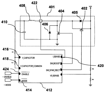
source 103 may include a resistor, active current source, switching supply or
other
mechanism. A switch 106 is open during charging. The switch 102 is modulated
to
maintain a fixed (maximum) voltage on the supercapacitor 104. This will
generally
be performed by a control mechanism (not shown).
[0005] When the main power source is lost, the switch 102 is opened and the
switch
106 is modulated to transfer energy from the supercapacitor 104 to Vcc via an
inductor 108 and a diode 110. Output filtering is performed by output
capacitors of
the main power supply (not shown). Thus there are separate charge and
discharge
circuits. This use of separate circuits for charge and discharge requires
additional part
count thereby adding cost, Printed Circuit Board (PCB) layout area and weight.
-1-
CA 02567562 2006-11-10
[0006] A higher efficiency can be achieved when the diode 110 has a switch
across it
to form a synchronous rectifier. A circuit having this additional component is
shown
in Figure 2. A switch 202 is connected in parallel with the diode 110.
However, the
circuit of Figure 2 has a separate charge and discharge circuit.
[0007] There are supercapacitor charging schemes of the art that only provide
for
simple charging mechanisms where the supercapacitor is placed directly across
the
voltage allowing a very large current at the start of charging.
[0008] There is therefore a need to provide a supercapacitor based backup
power
system that minimizes part count, provides efficient output voltage generation
and
provides controlled (the instantaneous current requirements of the voltage
source are
limited) and power-efficient charging of the supercapacitor.
SUMMARY OF THE INVENTION
[0009] The present invention generally relates to the charging and discharging
of a
supercapacitor that is used power supply backup situations.
[0010] It is an object of the invention to obviate or mitigate at least one of
the
drawbacks of prior art circuits used for the charging and discharging of a
supercapacitor.
[0011 ] In accordance with an aspect of the invention there is provided a
system for
backup power supply. The system includes a supercapacitor, and a single
circuit for
charging and discharging of the supercapacitor. The single circuit includes a
path
having an inductor for operating in charging mode for the charging and in
backup
mode for the discharging.
[0012] In accordance with another aspect of the invention, there is provided a
system
for backup power supply. The system includes a supercapacitor, an inductor, a
single
circuit operating with the inductor to provide for charging and discharging of
the
supercapacitor, and a controller for monitoring and controlling the single
circuit.
[0013] This summary of the invention does not necessarily describe all
features of the
invention.
-2-
CA 02567562 2006-11-10
BRIEF DESCRIPTION OF THE DRAWINGS
[0014] These and other features of the invention will become more apparent
from the
following description in which reference is made to the appended drawings
wherein::
[0015] FIGURE 1 is a schematic diagram illustrating a supercapacitor based
backup
power supply circuit of the prior art;
[0016] FIGURE 2 is a schematic diagram illustrating another supercapacitor
based
backup power supply circuit;
[0017] FIGURE 3 is a schematic diagram illustrating a supercapacitor based
backup
power supply circuit in accordance with an embodiment of the present
invention;
[0018] FIGURE 4 is a schematic diagram illustrating a supercapacitor based
backup
power supply circuit in accordance with another embodiment of the present
invention;
[0019] FIGURE 5 is a schematic diagram illustrating a supercapacitor based
backup
power supply circuit in accordance with a further embodiment of the present
invention;
[0020] FIGURE 6 is a schematic diagram illustrating an example of a control
circuit
in accordance with an embodiment of the present invention; and
[0021 ] FIGURE 7 is a schematic diagram illustrating a supercapacitor based
backup
power supply circuit in accordance with a further embodiment of the present
invention.
DETAILED DESCRIPTION
[0022] Embodiments of the present invention provide a backup power supply
which
is implemented by a single charge-discharge circuit for a supercapacitor. The
circuit
may have a reduced part count compared to circuits with separate charge and
discharge circuitry. In the description below, the term "connect(ed)" may be
used to
indicate that two or more elements are directly or indirectly in contact with
each other.
[0023] Figure 3 illustrates a supercapacitor based backup power supply circuit
in
accordance with an embodiment of the present invention. The backup power
supply
-3-
CA 02567562 2006-11-10
circuit 300 of Figure 3 includes switches 302 and 304, diodes 305 and 306, an
inductor 308, and a supercapacitor 310. The switch 302 is connected in
parallel with
the diode 305. The switch 304 is connected in parallel with the diode 306. The
inductor 308 and the supercapacitor 310 may be same or similar to the inductor
108
and the supercapacitor 104 of Figure 2, respectively. It is noted that Figure
3 is
conceptual in the sense that further circuitry around that presented in Figure
3 may be
included.
[0024] The diode 306 acts as a so-called free-wheeling diode. The combination
of the
switch 302, the inductor 308 and the diode 306 provides a switching power
supply or
so-called buck converter that can be used to charge the supercapacitor 310. As
this
circuit 300 can be used for charging, a current source and its controlling
switch (103
and 102 of Figure 2) become redundant. Therefore the circuit 300 does not use
the
current source 103 and its switch 102 of Figure 2. The circuit 300 provides
for both
charging and discharging of the supercapacitor 310 without a current source
and its
switch. In the circuit 300, magnetic element, i.e., inductor 308, operates in
a bi-
directional mode.
[0025] The circuit 300 is in charging mode when Vcc is generated by a main
power
supply (not shown). In charging mode, the switch 302 is modulated to charge
the
supercapacitor 310 to a desired level, i.e., power flows from Vcc to the
supercapacitor
310. In charging mode, the switch 304 is generally left open at this time. It
may
however be closed during the freewheeling time of the diode 306 for improved
efficiency. In this case the switch 304 behaves as a synchronous rectifier.
[0026] The circuit 300 is in backup (discharging) mode when the main power
source
that generates Vcc is detected as missing. In backup mode, the switch 304 is
modulated such that power flows from the supercapacitor 310 to Vcc. In backup
mode, the switch 302 is used as a synchronous rectifier and is closed during
the fly-
back time of the inductor 308.
[0027] In an embodiment, a controller is provided to the circuit 300 to
monitor the
main power source, supercapacitor voltage, output voltage (Vcc), inductor
current (if
current mode control is to be implemented), or combinations thereof, and then
control
-4-
CA 02567562 2006-11-10
the operation of the charge-discharge circuit based on the monitored value(s)
(e.g.,
Figures 4-6).
[0028] In one example, the controller monitors the main power source and
enables the
supercapacitor charging mechanism (charging mode) when the main power source
is
available. In charging mode, the controller monitors the voltage across the
supercapacitor 310 and operates the switches 302 and 304 in conjunction with
the
inductor 308 such that a buck converter (with synchronous rectifier) is
formed. In this
case energy flows from Vcc to the supercapacitor.
[0029] When the main power source is lost, the controller then switches to the
backup
mode. In backup mode, the controller monitors the voltage Vcc and runs the
switches
302 and 304 in conjunction with the inductor 308 such that a boost converter
(with
synchronous rectifier) is formed. In this case energy flows from the
supercapacitor to
Vcc.
[0030] In either charging or backup mode, the controller may implement the
current
mode control. The current mode control uses an inner control loop to limit the
peak
or average current in the inductor 308, which results in the apparent removal
of the
pole associated with the inductor 308 when compared to a voltage mode
controlled
switching mode power supply. This resulting reduced order transfer function
allows
for better dynamic response of the power supply, and may make the compensation
of
the power supply easier. For such control the controller includes a mechanism
to
monitor the current of the inductor 308 in the current control mode. The
inherent
control of inductor current from the current mode control works well with the
concept
of charging the capacitor at a fixed rate. The circuit 300 may employ a
voltage mode
control for controlling the output voltage.
[0031] The circuit 300 is appropriate for the configuration where the supply
voltage,
Vcc, is greater than or equal to the maximum allowable capacitor voltage.
However,
it is well understood by one skilled in the art that the circuit 300 can be
restructured
such that a Vcc lower than the maximum supercapacitor voltage can be
supported.
Thus a boost circuit to charge the supercapacitor, and a buck circuit to
supply Vcc in
backup is provided, i.e., a bi-directional power flow through one common
mechanism.
-5-
CA 02567562 2006-11-10
[0032] Figure 4 illustrates a supercapacitor based backup power supply circuit
in
accordance with a further embodiment of the present invention. The
supercapacitor
based backup power supply circuit 401 of Figure 4 is similar to the circuit
300 of
Figure 3. The circuit 401 includes switches 402 and 404, diodes 405 and 406,
inductor 408, and supercapacitor 410. The diodes 405 and 406 correspond to the
diodes 305 and 306 of Figure 3. The inductor 408 may be same or similar to the
inductor 308 of Figure 3. The supercapacitor 410 may be same or similar to the
supercapacitor 310 of Figure 3. The switches 402 and 404 correspond to the
switches
302 and 304 of Figure 3. However, in this embodiment the switch 402 and 404
are
Metal-Oxide-Semiconductor Field-Effect Transistors (MOSFETs). In the
description,
the terms "switch 402 (404)" and "MOSFET 402 (404)" may be used
interchangeably.
[0033] In one example, the diodes 405 and 406 may be intrinsic diodes of the
MOSFETs 402 and 404, respectively. In another example, the diodes 405 and 406
may be external schottky diodes connected in parallel with the intrinsic
diodes of the
MOSFETs 402 and 404, respectively. The schottky diode may provide a current
path
during the time it takes for the corresponding MOSFET to fully turn on. The
schottky
diode has a lower forward voltage than the parallel diode that is intrinsic to
the
construction of the MOSFET, which is efficient for use in power rectification
applications.
[0034] The diodes 405 and 406 and the switches 402 and 404 and an inductor
current
sensing mechanism may be integrated into an IC package (integrated circuit)
with a
controller 412. The controller 412 may be implemented in any appropriate
fashion.
The inductor 408 and the supercapacitor 410 may be outside of any integrated
circuit.
[0035] In order for the controller 412 to provide the required functionality
it receives
as input and is responsive to various signals. Such signals according to an
embodiment of the invention are presented in Figure 4. A "-MODE" control
signal
414 is used by the controller 412 to provide for automatic switchover between
charging and backup modes. In one example, the "-MODE" signal 414 is an
analogue input to a comparator (e.g., 600 of Figure 6) referenced to a voltage
compatible for TTL or some other logic level. This allows -MODE 414 to be
driven
from another circuit or from a scaled version of the main input power source.
In the
-6-
CA 02567562 2006-11-10
simplest realization, a resistive divider may scale the main input voltage to
the
comparator input, and may be scaled to less than the minimum input voltage,
allowing
backup in the case of unexpected supply removal. A"V_CAPACITOR" signal 416 is
a JFET input (low input current) and a"V_CAPACITOR_COMMON" signa1418 is
high impedance when not sampling the supercapacitor voltage, i.e., when in
backup
mode. A "-ENABLE" signal 424 is a signal to enable the entire functionality of
the
device.
[0036] A"I_SENSE" signal 420 is a single input allowing a current input as is
needed
in current mode control. In this embodiment, the current through the inductor
408 is
measured at a current sense 422. The current may in fact be measured in
several
places depending on the topology of circuit. The current sense mechanism of
the
controller 412 accepts bi-directional current flow assuming current mode
control is
used. In the embodiment, the circuit is operated at a high frequency allowing
the use
of a small inductor. For simple circuit realization, the internal reference
voltage of the
controller 412 may be less than both Vcc and the maximum voltage of the
supercapacitor 410.
[0037] The circuit 401 is appropriate for the configuration where the supply
voltage,
Vcc, is greater than or equal to the maximum allowable capacitor voltage. In
an
alternative embodiment the Vcc is lower than the maximum allowable capacitor
voltage. In this situation the topology of the charge-discharge circuit 401 of
Figure 4
is reversed so that a boost circuit charges the capacitor and a buck circuit
produces
Vcc from the capacitor voltage.
[0038] Figure 5 illustrates a supercapacitor backup power supply circuit in
accordance
with a further embodiment of the present invention. The configuration
presented in
Figure 5 is appropriate for a supercapacitor backup power supply with bi-
directional
power flow where Vcc is greater than the maximum supercapacitor voltage. The
controller element of this circuit includes diodes, power supply switches for
the
charge-discharge mechanism, current sensing, voltage sensing, and circuits to
support
the operation of the dual mode power supply. The controller element may be
implemented within an integrated circuit (referred to as integrated circuit
502). A
supercapacitor 504 and an inductor 506 are external of the integrated circuit
502.
-7-
CA 02567562 2006-11-10
[0039] The supercapacitor 504 may be same or similar to the supercapacitor 310
of
Figure 3 or the supercapacitor 410 of Figure 4. The inductor 506 may be
similar to
the inductor 308 of Figure 3 or the inductor 408 of Figure 4.
[0040] The circuit of Figure 5 has resistor networks similar to those of
Figure 4. A
resistor network having resistors 530 and 532 is provided between the
integrated
circuit 502 and a node 534 that is a connection node of the supercapacitor 504
and the
inductor 506. A resistor network having resistors 536 and 538 is provided
between
Vcc and the integrated circuit 502.
[0041 ] In Figure 5, only resistive elements in the feedback paths are shown,
which set
the DC potentials. The circuit of Figure 5 includes two feedback paths, only
one of
which is activated, depending on whether the supercapacitor 504 is being
charged
(i.e., charging mode), or discharged (i.e., backup mode). Compensation may be
achieved by the addition of capacitors to these resistors to provide spectral
shaping in
order to achieve stable operation of the circuit, in both charging and backup
modes. It
is understood by a person of ordinary skill in the art that more complex
feedback
mechanisms may be formed, depending on the desired operating characteristics
of the
circuit.
[0042] In Figure 5, the integrated circuit 502 includes a plurality of pins
for
INDUCTOR signal 510, V_CAPACITOR signa1512, V_CAPACITOR COMMON
signa1514, -ENABLE signa1516, -MODE signa1518, VCC signa1520, V_SENSE
signa1522 and GROUND signal 524. The INDUCTOR signa1510, the
V_CAPACITOR signal 512, the V_CAPACITOR COMMON signal 514, the
-ENABLE signal 516, the -MODE signal 518, and the V_SENSE signal 522 may be
similar to the I_SENSE signal 420, the V CAPACITOR signal 418, the
V_CAPACITOR COMMON signa1418, the -ENABLE signa1424, the -MODE
signa1414, and the VO_SENSE signal in Figure 4, respectively.
[0043] Figure 6 illustrates an example of a control circuit in accordance with
an
embodiment of the present invention. The pin-out of the circuit of Figure 6 is
similar
to the controller of Figure 5. In Figure 6, signals associated with the
integrated circuit
502 other than the -ENABLE signa1516 are shown as examples. The circuit of
-8-
CA 02567562 2006-11-10
Figure 6 is a basic current mode control and, for simplicity, compensation
(feedback)
elements of the control loops are not shown.
[0044] The -MODE input 518 is used to define the operating mode of the circuit
(charging or backup) and select the source of the voltage error amplifier
(i.e., 602 or
604) into the inner current loop through a switch 606. A comparator 600
compares
the -MODE input 518 with a certain voltage and operates the switch 606. A
comparator 608 compares the output of the switch 606 and the output of an
"ISENSE"
circuit 616.
[0045] The circuit 616 includes a resistor 617 and a magnitude and level shift
circuit
618. The circuit 616 measures the current flowing through the inductor
connected at
the INDUCTOR node 510. In this embodiment, this measurement is a high-side
measurement, and the sensing element is not referred to ground. The circuit
616 thus
includes a mechanism to transmit the measured value to the ground-referenced
comparator 608 in order to implement current mode control. The magnitude of
the
current flow operates the comparator 608. When the inductor current hits a
threshold,
e.g., its peak current for the current mode, the current mode is activated.
[0046] A latch 610 includes "S" node connected to a clock circuit 612, "R"
node
connected to the output of the comparator 608, and "Q" node connected to a
gate
drive circuit 614. The gate drive circuit 614 selects the correct switch
operation for
the operating mode (charging or backup), including operation of the
synchronous
rectifier. In Figure 6, the gate drive circuit 614 drives switches 620, 622
and 624.
[0047] The switch 620 is turned on during the supercapacitor-charging mode. In
backup mode, the switch 620 is turned off so the resistor network with
resistors 530
and 532 of Figure 5 does not bleed off energy in order to maximize the backup
time
available. Granted the power bled off may tend to be small, and thus the
switch 620
may be eliminated at the expense of slightly reduced backup time.
[0048] The nature of the ISENSE circuitry (616, 618) depends on how the
circuit is
constructed. A current transformer is the simplest mechanism if building the
circuit
using discrete parts. For silicon implementations, techniques to do high-side
current
measurements are available to IC designers.
-9-
CA 02567562 2006-11-10
[0049] In the above embodiments, the main power supply has sufficient hold-up
time
such that the backup supply (i.e., the supercapacitor 310 of Figure 3 or 410
of Figure
4) can detect the missing input power and enter the backup mode from the
charging
mode.
[0050] In a further embodiment, the intrinsic diodes of the MOSFETs may be
used in
lieu of synchronous rectification.
[0051 ] In a further embodiment, additional inputs may be provided to set the
peak
inductor current for charging and discharging the supercapacitor, and for
compensation of the control loop(s).
[0052] Figure 7 illustrates a supercapacitor based backup power supply circuit
in
accordance with a further embodiment of the present invention. The backup
power
supply circuit 700 of Figure 7 is suitable for the configuration where the
supply
voltage, Vcc, is less than or equal to the maximum allowable capacitor
voltage.
[0053] The supply circuit 700 includes switches 702 and 704, diodes 705 and
706, an
inductor 708, and a supercapacitor 710. The switch 702 is connected in
parallel with
the diode 705. The switch 704 is connected in parallel with the diode 706. The
inductor 708 and the supercapacitor 710 may be same or similar to the inductor
308
and the supercapacitor 304 of Figure 3, respectively. In the backup power
supply
circuit 700, the switch 702 and the diode 705 are provided between the
inductor 708
and the supercapacitor 710. The inductor 708 is connected to Vcc node.
[0054] In charging mode, the switch 704 is a power switch for the boosting and
the
switch 702 acts as a synchronous rectifier. In backup mode, the switch 702 is
a power
switch 702 is a power switch for the bucking and the switch 704 acts as a
synchronous
rectifier.
[0055] It will be appreciated by a person of ordinary skill in the art that
the topology
of the based backup power supply circuit is not limited to those of Figures 3,
4 and 7
and other topologies can be envisioned.
[0056] The present invention has been described with regard to one or more
embodiments. However, it will be apparent to persons skilled in the art that a
number
-10-
CA 02567562 2006-11-10
of variations and modifications can be made without departing from the scope
of the
invention as defined in the claims.
-11-