Note: Descriptions are shown in the official language in which they were submitted.
CA 02567696 2006-11-22
WO 2005/123395 PCT/AU2005/000455
PROCESS FOR MODIFYING THE SURFACE PROFILE OF AN INK SUPPLY CHANNEL IN A
PRINTHEAD
Field of the Invention
This invention relates to a process for modifying the surface profile of an
ink supply channel in a
printhead. It has been developed primarily to minimize angular sidewall
projections in the ink supply channels,
which can disrupt the flow of ink.
Cross reference to related application
The following patents or patent applications filed by the applicant or
assignee of the present invention are
hereby incorporated by cross-reference.
6750901 6750901 6476863 6788336 11/003786 11/003354 11/003616
11/003418 11/003334 11/003600 11/003404 11/003419 11/003700 11/003601
11/003618 11/003615 11/003337 11/003698 11/003420 11/003682 11/003699
CAA018US 11/003463 11/003701 11/003683 11/003614 11/003702 11/003684
11/003619 11/003617 6623101 6406129 6505916 6457809 6550895
6457812 IJ52NPUS 6428133 10/815625 10/815624 10/815628 10/913375
10/ 913 3 7 3 10/913 3 74 10/913 3 72 10/913 3 7 7 10/913 3 7 8 10/913 3 8 0
10/913 3 79
10/913376 10/913381 10/986402 10/407212 10/760272 10/760273- 10/760187
10/760182 10/760188 10/760218 10/760217 10/760216 10/760233 10/760246
10/760212 10/760243 10/760201 10/760185 10/760253 10/760255 10/760209
10/760208 10/760194 10/760238 10/760234 10/760235 10/760183 10/760189
10/760262 10/760232 10/760231 10/760200 10/760190 10/760191 10/760227
10/760207 10/760181 10/728804 10/728952 10/728806 10/728834 10/729790
10/728884 10/728970 10/728784 10/728783 10/728925 10/728842 10/728803
10/728780 10/728779 10/773189 10/773204 10/773198 10/773199 6830318
10/773201 10/773191 10/773183 10/773195 10/773196 10/773186 10/773200
10/773185 10/773192 10/773197 10/773203 10/773187 10/773202 10/773188
10/773194 10/773193 10/773184 11/008118 MTB38US MTB39US 10/727181
10/727162 10/727163 10/727245 10/727204 10/727233 10/727280 10/727157
10/727178 10/727210 10/727257 10/727238 10/727251 10/727159 10/727180
10/727179 10/727192 10/727274 10/727164 10/727161 10/727198 10/727158
10/754536 10/754938 10/727227 10/727160 10/934720 PECOINPUS 6795215
10/296535 09/575109 6805419 6859289 09/607985 6398332 6394573
6622923 6747760 10/189459 10/884881 10/943941 10/949294 10/039866
10/854521 10/854522 10/854488 10/854487 10/854503 10/854504 10/854509
CA 02567696 2006-11-22
WO 2005/123395 PCT/AU2005/000455
2
10/854510 10/854496 10/854497 10/854495 10/854498 10/854511 10/854512
10/854525 10/854526 10/854516 10/854508 10/854507 10/854515 10/854506
10/854505 10/854493 10/854494 10/854489 10/854490 10/854492 10/854491
10/854528 10/854523 10/854527 10/854524 10/854520 10/854514 10/854519
PLT036US 10/854499 10/854501 10/854500 10/854502 10/854518 10/854517
10/934628 10/760254 10/760210 10/760202 10/760197 10/760198 10/760249
10/760263 10/760196 10/760247 10/760223 10/760264 10/760244 10/760245
10/760222 10/760248 10/760236 10/760192 10/760203 10/760204 10/760205
10/760206 10/760267 10/760270 10/760259 10/760271 10/760275 10/760274
10/760268 10/760184 10/760195 10/760186 10/760261 10/760258 11/014764
RRB002US 11/014748 11/014747 11/014761 11/014760 11/014757 11/014714
11/014713 RRB010US 11/014724 11/014723 11/014756 11/014736 11/014759
11/014758 11/014725 11/014739 11/014738 11/014737 11/014726 11/014745
11/014712 11/014715 11/014751 11/014735 11/014734 RRB030US 11/014750
11/014749 11/014746 11/014769 11/014729 11/014743 11/014733 RRC005US
11/014755 11/014765 11/014766 11/014740 11/014720 RRCOI lUS 11/014752
11/014744 11/014741 11/014768 RRC016US 11/014718 11/014717 11/014716
11/014732 11/014742 09/575197 09/575197 09/575195 09/575159 09/575132
09/575130 09/575165 6813039 09/575118 09/575131 09/575116 6816274
09/575139 09/575186 6681045 6728000 09/575145 09/575192 09/575181
09/575193 09/575183 6789194 09/575150 6789191 6644642 6502614
6622999 6669385 6549935 09/575187 6727996 6591884 6439706
6760119 09/575198 6290349 6428155 6785016 09/575174 6822639
6737591 09/575154 09/575129 6830196 6832717 09/575189 09/575170
09/575171 09/575161 09/575123 6825945
Some applications have been listed by docket numbers. These will be replaced
when application numbers are
known.
Background of the Invention
The impact of MEMS (Microelectromechanical Systems) devices on the
microelectronics industry has
been extremely significant in recent years. Indeed, MEMS is one of the fastest
growing areas of microelectronics.
The growth of MEMS has been enabled, to a large extent, by the extension of
silicon-based photolithography to
the manufacture of micro-scale mechanical devices and structures.
Photolithographic techniques, of course, rely
on reliable etching techniques, which allow accurate etching of a silicon
substrate revealed beneath a mask.
MEMS devices have found applications in a wide variety of fields, such as in
physical, chemical and
biological sensing devices. One important application of MEMS devices is in
inkjet printheads, where micro-scale
CA 02567696 2006-11-22
WO 2005/123395 PCT/AU2005/000455
3
actuators for inkjet nozzles may be manufactured using MEMS techniques. The
present Applicant has developed
printheads incorporating MEMS ink ejection devices and these are described in
the following patents and patent
applications, all of which are incorporated herein by reference.
6,227,652 6,213,588 6,213,589 6,231,163 6,247,795
6,394,581 6,244,691 6,257,704 6,416,168 6,220,694
6,257,705 6,247,794 6,234,610 6,247,793 6,264,306
6,241,342 6,247,792 6,264,307 6,254,220 6,234,611
6,302,528 6,283,582 6,239,821 6,338,547 6,247,796
6,557,977 6,390,603 6,362,843 6,293,653 6,312,107
6,227,653 6,234,609 6,238,040 6,188,415 6,227,654
6,209,989 6,247,791 6,336,710 6,217,153 6,416,167
6,243,113 6,283,581 6,247,790 6,260,953 6,267,469
6,273,544 6,309,048 6,420,196 6,443,558 6,439,689
6,378,989 6,848,181 6,634,735 6,623,101 6,406,129
6,505,916 6,457,809 6,550,895 6,457,812 6,428,133
6,362,868 6,755,509
Typically a MEMS inkjet printhead ("MEMJET printhead") is comprised of a
plurality of chips, with
each chip having several thousand nozzles. Each nozzle comprises an actuator
for ejecting ink, which may be, for
example, a thermal bend actuator (e.g. US 6,322,195) or a bubble-forming
heater element actuator (e.g. US
6,672,709). The chips are manufactured using MEMS techniques, meaning that a
high nozzle density and, hence,
high resolution printheads can be mass-produced at relatively low cost.
In the manufacture of MEMS printhead chips, it is often required to perform
deep or ultradeep etches.
Etch depths of about 3 pm to 10 um may be termed "deep etches", whereas etch
depths of more than about 10 fmn
may be termed "ultradeep etches.
MEMS printhead chips typically require delivery of ink to each nozzle through
individual ink supply
channels having a diameter of about 20 pm. These ink channels are typically
etched through wafers having a
thickness of about 200 pm, and therefore place considerable demands on the
etching method employed. It is
especially important that each ink channel is perpendicular to the wafer
surface and does not contain kinks,
sidewall projections (e.g. grassing) or angular junctions, which can interfere
with the flow of ink.
In the Applicant's US patent application nos. 10/728,784 (Applicant Ref:
MTB08) and 10/728,970
(Applicant Ref: MTB07), both of which are incorporated herein by reference,
there is described a method of
fabricating inkjet printheads from a wafer having a drop ejection side and an
ink supply side. Referring to Figure
1, there is shown a typical MEMS nozzle arrangement 1 comprising a bubble-
forming heater element actuator
assembly 2. The actuator assembly 2 is formed in a nozzle chamber 3 on the
passivation layer 4 of a silicon wafer
CA 02567696 2006-11-22
WO 2005/123395 PCT/AU2005/000455
4
5. The wafer typically has a thickness "B" of about 200 pm, whilst the nozzle
chamber typically occupies a
thickness "A" of about 20 pm.
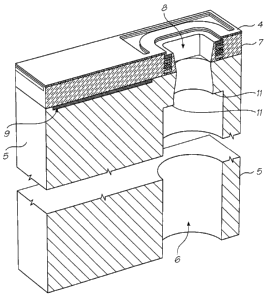
Referring to Figure 2, an ink supply channel 6 is etched through the wafer 5
to the CMOS metallization
layers of an interconnect 7. An inlet 8 provides fluid connection between the
ink supply channel 6 and the nozzle
chamber (removed for clarity in Figure 2). CMOS drive circuitry 9 is provided
between the wafer 5 and the
interconnect 7. The actuator assembly 2, associated drive circuitry 9 and ink
supply channel 6 may be formed on
and through a wafer 3 by lithographically masked etching techniques, as
described in US application no.
10/302,274, which is incorporated herein by reference.
Referring to Figure 3, the ink supply channel 6 is formed in the wafer 5 by
fust etching a trench partially
through the wafer 5 from the drop ejection side (i.e. nozzle side) of the
wafer. (This trench will become the inlet 8,
shown in Figure 2). Once formed, the trench is plugged with photoresist 10, as
shown in Figure 3, and the ink
supply channel 6, is formed by ultradeep etching from the ink supply side of
the wafer 5 to the photresist plug 10.
Finally, the photoresist 10 is stripped from the trench to form the inlet 8,
which provides fluid connection between
the ink supply channel 6 and the nozzle chamber 3.
This "back-etching" technique avoids filling and removing an entire 200,um
long ink supply channel
with resist whilst nozzle structures in the wafer are being lithographically
formed. However, there are a number of
problems associated with back-etching the ink supply channels in this way.
Firstly, the mask on the ink supply
side needs to be carefully aligned so that the etched channels meet the
trenches plugged with photoresist, and do
not damage the drive circuitry 9. Secondly, the etching needs to be
perpendicular and anisotropic to a depth of
about 200 pm. Thirdly, angular sidewall features in the ink channel,
especially at the junction of the ink channel 6
with the inlet 8, are produced. These angular shoulders should ideally be
minimized to allow smooth ink flow.
Accordingly, there is a demand for improved etching methods, which allow
ultradeep trenches having relatively
smooth sidewalls to be made in silicon wafers.
Several methods for etching ultradeep trenches into silicon are known in the
art. All these methods
involve deep reactive ion etching (DRIE) using a gas plasma. The semiconductor
substrate, with a suitable mask
disposed thereon, is placed on a lower electrode in a plasma reactor, and
exposed to an ionized gas plasma formed
from a mixture of gases. The ionized plasma gases (usually positively charged)
are accelerated towards the
substrate by a biasing voltage applied to the electrode. The plasma gases etch
the substrate either by physical
bombardment, chemical reaction or a combination of both. Etching of silicon is
usuaily ultimately achieved by
formation of volatile silicon halides, such as SiF4, which are carried away
from the etch front by a light inert
carrier gas, such as helium.
Anisotropic etching is generally achieved by depositing a passivation layer
onto the base and sidewalls of
the trench as it is being formed, and selectively etching the base of the
trench using the gas plasma.
One method for achieving ultradeep anisotropic etching is the "Bosch process",
described in US
5,501,893 and US 6,284,148. This method involves alternating polymer
deposition and etching steps. After
formation of a shallow trench, a first polymer deposition step deposits a
polymer onto the base and side walls of
the trench. The polymer is deposited by a gas plasma formed from a fluorinated
gas (e.g. CHF3, C4Fg or C2F4) in
CA 02567696 2006-11-22
WO 2005/123395 PCT/AU2005/000455
the presence or in the absence of an inert gas. In the subsequent etching
step, the plasma gas mix is changed to
SF6/Ar. The polymer deposited on the base of the trench is quickly broken up
by ion assistance in the etching step,
while the sidewalls remain protected. Hence, anisotropic etching may be
achieved. However, a major
disadvantage of the Bosch process is that polymer deposition and etching steps
need to be alternated, which means
5 continuously alternating the gas composition of the plasma. This
alternation, in turn, leads to uneven trench
sidewalls, characterized by scalloped surface formations.
At worst, the Bosch process tends to leave grass-like spikes in the sidewalls
of the trenches due to
incomplete removal of the polymer passivation layer. These grass-like residues
are especially undesirable in ink
supply channels, because ink flow through the channels may break off the
grassy spikes and block the ink nozzles
downstream. Furthermore, sharp sidewall projections create air pockets in the
ink, which can lead to poor ink flow
and, hence, poor print quality and/or nozzle blocking.
A modification of the cyclical Bosch process is described in US 6,127,278,
assigned to Applied
Materials, Inc. In the Applied Materials process, a first passivation etch is
performed using a HBr/02 plasma,
followed by a main etch using a SF6/HBr/02 in alternating succession. The HBr
enhances passivation, probably by
formation of relatively nonvolatile silicon bromides in the passivation layer.
However, this cyclical
passivation/etching process still suffers from grassing and scalloped
sidewalls, which are evident in the Bosch
process.
Another ultradeep anisotropic etching process is the "Lam process", described
in US 6,191,043. The Lam
process utilizes a constant, non-alternating plasma gas chemistry of SF6/01-
/Ar/He and achieves simultaneous
sidewall passivation during the etch. To some extent, this avoids the problems
of scalloped sidewalls and grassing
resulting from cyclical etching processes.
However, there is still a need to improve the surface profiles of ultradeep
trenches in order to minimize
the deleterious effects of grassing and scalloped sidewalls. It would be
especially desirable to minimize angular
junctions between nozzle inlets and ink supply channels in printheads. As
discussed above, angular shoulder
junctions are a common problem when "back-etching" ink supply channels from
the ink supply side of printhead
wafers.
Summarv of the Invention
In a first aspect, the present invention provides a process for modifying the
surface profile of an ink
supply channel in a printhead, said process comprising the steps of:
(i) providing a printhead comprising at least one ink supply channel; and
(ii) ion milling the at least one ink supply channel.
In a second aspect, the present invention provides a method of fabricating an
inkjet printhead comprising
a plurality of nozzles, ejection actuators, associated drive circuitry and ink
supply channels, said method
comprising the steps of:
(i) providing a wafer having a drop ejection side and an ink supply side;
(ii) etching a plurality of trenches partially through said drop ejection side
of said wafer;
CA 02567696 2006-11-22
WO 2005/123395 PCT/AU2005/000455
6
(iii) filling said trenches with photoresist;
(iv) forming a plurality of corresponding nozzles, ejection actuators and
associated drive circuitry on
said drop ejection side of said wafer using lithographically masked etching
techniques;
(v) etching a plurality of corresponding ink supply channels from said ink
supply side of said wafer to
said photoresist;
(vi) modifying the surface profiles of said ink supply channels by ion
milling; and
(vii) stripping said photoresist from said trenches to form nozzle inlets,
thereby providing fluid
connection between said ink supply side and said nozzles.
In a third aspect, the present invention provides an inkjet printhead
comprising:
a wafer having a drop ejection side and an ink supply side;
a plurality of nozzles fonned on said drop ejection side, each of said nozzles
having a
corresponding inlet in said wafer; and
a plurality of corresponding ink supply channels leading to each inlet from
said ink supply side,
wherein shoulders defined by the junction of said ink supply channels with
said inlets are tapered and/or rounded.
Hitherto, the importance of the surface profile of ink supply channels in
printheads fabricated by MEMS
techniques had not been fully appreciated. Whilst several ultradeep etching
techniques have become available in
recent years, none of these addresses the problems of grassing, scalloped
sidewalls and/or angular shoulder
junctions between nozzle inlets and ink supply channels. The present invention
introduces an additional surface
profile modifying step into the printhead manufacturing process, which has the
effect of tapering and/or rounding
angular surface features in the sidewalls of ink supply channels. Hence,
printheads made by the process of the
present invention generally exhibit improved ink flow through their ink supply
channels.
Optionally, angular surface features in the sidewalls of ink supply channels
are tapered and/or rounded
by the ion milling. An angular surface feature may be, for example, a spike
projecting inwardly from a sidewall.
Alternatively, it may be an angled shoulder at the point where the ink supply
channel narrows into a nozzle inlet.
The process of the present invention advantageously tapers these angular
surface features, such that they are
generally rounded or smoothed off. Hence, ink flowing past these features
approaches a curved surface rather than
an angular surface. This means that the ink can flow smoothly past, without
generating excessive turbulence
and/or air bubbles in pockets behind jutting projections where ink is flowing
relatively slowly.
Typically, the ink supply channel itself is formed by anisotropic ultradeep
etching of a semiconductor
(e.g. silicon) wafer. Any known anisotropic ultradeep etching technique, such
as those described above, may be
used to form the ink supply channels.
Optionally, the ion milling is performed in a plasma etching reactor, such as
an inductively coupled
plasma etching reactor. Plasma etching reactors are well known in the art and
are commercially available from
various sources (e.g. Surface Technology Systems, PLC). Typically, the etching
reactor comprises a chamber
formed from aluminium, glass or quartz, which contains a pair of parallel
electrode plates. However, other designs
of reactor are available and the present invention is suitable for use with
any type of plasma etching reactor.
CA 02567696 2006-11-22
WO 2005/123395 PCT/AU2005/000455
7
A radiofrequency (RF) energy source is used to ionize a plasma gas (or gas
mixture) introduced into the
chamber. The ionized gas is accelerated towards a substrate disposed on a
lower electrode (electrostatic chuck) by
a biasing voltage. In the present invention, etching is typically achieved
purely by physical bombardment of the
substrate. Various control means are provided for controlling the biasing
voltage, the RF ionizing energy, the
substrate temperature, the chamber pressure etc. It will, of course, be within
the ambit of the skilled person's
common general knowledge to vary plasma reactor parameters in order to
optimize etching conditions.
Optionally, the ion milling is perfonned using a heavy inert gas selected from
argon, krypton or xenon.
Preferably, the inert gas is argon since this is widely available at
relatively low cost, and, because of its relatively
high mass, has excellent sputtering properties. Typically, an argon ion plasma
is generated in a plasma etching
reactor, and the argon ions accelerated perpendicularly towards a silicon
wafer having ink supply channels etched
therein.
The ion milling may be performed at any suitable pressure. Typically, the
pressure will be in the range of
5 to 2000 mTorr. In other words, ion milling may be performed at low pressure
(about 5 to 250 mTorr) or high
pressure (about 250 to 2000 mTorr).
Low pressure ion milling has the advantage that most commercially available
plasma etching reactors are
configured for low pressure etching. Hence, low pressure ion milling does not
require any special apparatus.
However, ion milling may also be performed at high pressure. High pressure ion
milling has the
advantage that steeper tapering is usually obtainable. The principle of using
a high pressure ion milling to produce
steep taper angles may be understood as follows. Normally, sputter etching is
performed at relatively low
pressures (e.g. about 50 to 250 mTorr) to achieve high sputter etching
efficiency. Such a low pressure produces a
nearly collision-free path for silicon atoms sputtered from the surface,
thereby optimizing etching efficiency.
By sputter etching at high pressure rather than low pressure, the mean free
path of sputtered silicon atoms
is reduced, because sputtered (reflected) silicon atoms have a greater chance
of colliding with incoming argon
ions in the plasma gas. The result is that a gaseous cloud is formed above the
substrate surface, which redeposits
reflected silicon atoms back onto the silicon surface. There is an increasing
net deposition of reflected silicon
atoms at greater depths, which results in angular surface features in the
sidewalls becoming more tapered.
US 5,888,901, which is incorporated herein by reference, describes high
pressure ion milling of a Si02
dielectric surface using argon as the sputtering gas. Whilst the method
described in US 5,888,901 is used for
tapering a SiO2 dielectric surface layer, rather than tapering angular surface
features on the sidewalls of ultradeep
channels etched into silicon, this method may be readily modified and applied
to the process of the present
invention.
Low pressure ion milling is generally preferred in the present invention,
because it is usually only
necessary to round off angular sidewall features in order to achieve improved
ink flow, rather than taper the whole
sidewall feature. Moreover, low pressure ion milling does not require any
special apparatus and can therefore be
easily incorporated into a typical printhead fabrication process.
CA 02567696 2006-11-22
WO 2005/123395 PCT/AU2005/000455
8
Optionally, each ink supply channel has a depth in the range of 100 to 300
Enn, optionally 150 to 250 fan,
or optionally about 200 ,um. Optionally, each ink supply channel has a
diameter in the range of 5 to 30,um,
optionally 14 to 28 pm, or optionally 17 to 25 um.
Optionally, each nozzle inlet has a depth in the range of 5 to 40 ,um,
optionally 10 to 30 ~cm, or optionally
15 to 25,um. Optionally, each nozzle inlet has a diameter in the range of 3 to
28 ,um, optionally 8 to 24 pm, or
optionally 12 to 20 ,um.
Usually, each ink supply channel has a larger diameter than its corresponding
nozzle inlet, and the
process of the present invention may be used to taper angular shoulders
defined by the junction of the inlet and the
channel.
Brief Description of the Drawings
Figure 1 shows a perspective view of a prior art printhead nozzle arrangement
for a printhead;
Figure 2 is a cutaway perspective view of the prior art printhead nozzle
arrangement shown in Figure 1,
with the actuator assembly removed and the ink supply channel exposed;
Figure 3 is a cutaway perspective view of the printhead nozzle arrangement
shown in Figure 2 before
stripping away the photoresist plug; and
Figure 4 is a cutaway perspective view of a printhead nozzle arrangement
according to the present
invention, with the actuator assembly removed and the ink supply channel
exposed.
Detailed Description of a Preferred Embodiment
Figure 2 shows a prior art printhead nozzle arrangement having angular
shoulders 11, which define a
junction between the ink supply channel 6 and the inlet 8. These angular
shoulders are formed by prior art
ultradeep etching methods described above and in the Applicant's US patent
application nos. 10/728,784
(Applicant Ref: MTB08) and 10/728,970 (Applicant Ref: MTB07), both of which
are incorporated herein by
reference.
Referring to Figure 3, there is shown an ink supply channel 6 before removal
of the photoresist plug 10.
The channel 6 is etched partially beyond and around the photoresist plug 10.
In accordance with the present
invention, at this stage of printhead fabrication, the wafer is subjected to
argon ion milling in a plasma etching
reactor. Optimal operating parameters of the plasma etching reactor may be
readily determined by the person
skilled in the art.
During the argon ion milling, the angular shoulders 11 are tapered by
simultaneously etching and
redepositing sputtered silicon back onto the sidewalls of the channel. The
result is a printhead nozzle arrangement
as shown in Figure 4, having tapered shoulders 12, which define the junction
between the inlet 8 and the ink
supply channel 6.
Depending on the pressure, the bias power and/or the milling time, the
shoulders may be either fully
tapered (as shown in Figure 4) or merely partially rounded. In either case,
the removal of sharply angled shoulders
CA 02567696 2006-11-22
WO 2005/123395 PCT/AU2005/000455
9
11 generally improves ink flow through the channel 6 and minimizes pockets of
turbulence and/or air bubble
formation.
It will, of course, be appreciated that the present invention has been
described purely by way of example
and that modifications of detail may be made within the scope of the
invention, which is defined by the
accompanying claims.