Note: Descriptions are shown in the official language in which they were submitted.
CA 02567818 2006-11-23
WO 2005/117329 PCT/US2005/016026
[0001] DATA-MOVER CONTROLLER WITH PLURAL
REGISTERS FOR SUPPORTING CIPHERING OPERATIONS
[0002] FIELD OF THE INVENTION
[0003] The present invention relates to the field of data processing which
may be used for wireless communication applications. More specifically, the
present invention relates to the ciphering and transferring of data between
two
different types of memory devices using a data-mover controller and a
ciphering
engine.
[0004] BACKGROUND
[0005] Many early Third Generation Partnership Project (3GPP) modems
implement the layer 1 protocol in software. As data rates have increased, the
need for hardware support for some functions has been required. In wireless
communication systems such as 3GPP, Global System for Mobile
Communications (GSM) and Universal Mobile Telecommunications Systems
(UMTS), hardware modules have recently been introduced to act as accelerators
for some of the more compute-intensive operations.
[0006] One such operation is ciphering, whereby the manipulation of
encryption keys and the actual encryption of data increases required
processing
capacity in proportion to the amount of data being manipulated. Within the
security architecture of a 3GPP system, there are two standardized algorithms:
a
confidentially cipher algorithm "f8" and an integrity cipher algorithm "f9".
[0007] A means for efficiently performing ciphering calculations while data
is being moved from one memory (i.e., layer) to another is desired.
[0008] SUMMARY
[0009] A data processing system ciphers and transfers data between a
first memory unit and a second memory unit, such as, for example, between a
share memory architecture (SMA) static random access memory (SRAM) and a
double data rate (DDR) synchronous dynamic random access memory (SDRAM).
The system includes a ciphering engine and a data-mover controller. The data-
-1-
CA 02567818 2006-11-23
WO 2005/117329 PCT/US2005/016026
mover controller includes at least one register having a field that specifies
whether or not the transferred data should be ciphered by the ciphering
engine.
[0010] If the field specifies that the transferred data should be ciphered,
the field may also specify the type of ciphering that is to be performed by
the
ciphering engine, such as a 3GPP standardized confidentially cipher algorithm
"18" or integrity cipher algorithm "fl9".
[0011] The register may include another field which specifies a message
authentication code (MAC) value calculated by the standardized integrity
cipher
algorithm fl9 calculation.
[0012] The register may include yet another field which specifies whether
data is moved from the first memory unit to the second memory unit, or from
the
second memory unit to the first memory unit. The first and second memory units
may differ in processing speed.
[0013] The register may include yet another field which specifies the size of
a block of data to be transferred by the data-mover controller. The data block
size may be four bytes, eight bytes, sixteen bytes or thirty-two bytes.
[0014] The register may include yet another field which specifies the
number of data blocks to be transferred by the data-mover controller.
[0015] The register may include yet another field which specifies whether
an interrupt pulse should be generated when the transfer of data is completed.
[0016] The register may include yet another field which specifies a value
embedded in a cipher header and processed by the ciphering engine.
[0017] The register may include yet another field which specifies an
encryption length.
[0018] The register may include yet another field which specifies a value
embedded in an encrypted header and processed by the ciphering engine.
[0019] The register may include yet another field which specifies a key
used by the ciphering engine for ciphering the data as it is moved. The key
may
be a 128-bit key.
-2-
CA 02567818 2006-11-23
WO 2005/117329 PCT/US2005/016026
[0020] BRIEF DESCRIPTION OF THE DRAWINGS
[0021] A more detailed understanding of the invention may be had from the
following description, given by way of example and to be understood in
conjunction with the accompanying drawings wherein:
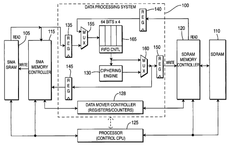
[0022] Fig. 1 is a diagram of a data processing system for ciphering and
transferring data from one memory to another in accordance with a preferred
embodiment of the present invention;
[0023] Fig. 2 shows an exemplary configuration of registers incorporated
into a data-mover controller;
[0024] Fig. 3 shows a register defining the data-mover controller starting
address for source accesses from SDRAM;
[0025] Fig. 4 shows a register defining the data-mover controller starting
address for destination accesses to SDRAM;
[0026] Fig. 5 shows a register defining the data-mover controller starting
address for source accesses to SMA memory;
[0027] Fig. 6 shows a register defining the data-mover controller starting
address for destination accesses to SMA memory;
[0028] Fig. 7 shows a register defining the number of blocks to be moved
between SDRAM and SMA memory;
[0029] Fig. 8 shows a register specifying the mode of the data-mover
controller;
[0030] Fig. 9 shows a register defining a count value embedded in a cipher
head;
[0031] Fig. 10 shows a register defining a fresh value embedded in the
cipher head;
[0032] Fig. 11 shows a register defining a bearer and direction value that
must be placed in the encrypted header and the total number of bits to be
encrypted;
[0033] Fig. 12 shows a register defining a 128-bit key used for ciphering
during data movement; and
-3-
CA 02567818 2006-11-23
WO 2005/117329 PCT/US2005/016026
[0034] Fig. 13 shows a register which provides a calculated Message
Authentication Code (MAC) value.
[0035] DETAILED DESCRIPTION OF THE PREFERRED EMBODIMENT(S)
[0036] The preferred embodiments will be described with reference to the
drawing figures where like numerals represent like elements throughout.
[0037] Preferably, the present invention disclosed herein is incorporated
into a wireless transmit/receive unit (WTRU) and/or a Node B. However, it is
envisioned that the just about any wireless communication scheme could benefit
from the present invention.
[0038] Hereinafter, a WTRU includes but is not limited to a user
equipment, mobile station, fixed or mobile subscriber unit, pager, or any
other
type of device capable of operating in a wireless environment. Furthermore, a
Node B includes, but is not limited to, a base station, site controller,
access point
or other interfacing device in a wireless environment.
[0039] The features of the present invention may be incorporated into an
integrated circuit (IC) or be configured in a circuit comprising a multitude
of
interconnecting components.
[0040] The present invention is applicable to communication systems using
time division duplex (TDD), frequency division duplex (FDD), code division
multiple access (CDMA), CDMA 2000, time division synchronous CDMA
(TDSCDMA), orthogonal frequency division multiplexing (OFDM) or the like.
[0041] The present invention, like many other modem implementations,
has hardware modules (accelerators) to implement data processing functions.
The present invention uses a shared memory to reduce the number of existing
memory instances. Hardware modules and a processor access this memory.
[0042] By using a single memory versus many small dedicated memories,
the die size of an Application-Specific Integrated Circuit (ASIC) version of a
circuit, such as for a modem or the like, is reduced. This memory typically
needs
to be very fast. Fast memory (SRAM) is typically very expensive and is not as
dense, from an area point of view, as other forms of memory, i.e., DRAM. See,
-4-
CA 02567818 2006-11-23
WO 2005/117329 PCT/US2005/016026
for example, U.S. Patent Application No.10/414,125, filed Apri115, 2003,
entitled
"Software Parameterizable Control Blocks For Use In Physical Layer
Processing," which is incorporated by reference as if fully set forth.
[0043] The present invention also has other memory available to the
processor to store large amounts of data. This memory is implemented by an
external, commercially available DRAM or SDRAM chip. Reordering queues
and other buffers for storage of data being processed for applications are
examples of the uses for this larger, slower memory.
[0044] In accordance with the present invention, a data-mover controller
has been configured as a hardware accelerator in the movement of data between
the fast, hardware accessible memory (SRAM) and the slower, denser memory
(DRAM). Not having the hardware accelerator would mean that the processor
would have to use a software loop to shuffle the data around, thus expending a
large portion of the processor's calculating resources, as measured by
Millions of
Instructions Per Second (MIPS).
[0045] Data is often moved in blocks called Protocol Data Units (PDUs) and
Service Data Units (SDUs). These blocks can be encrypted per the 3GPP
standard. The process of encrypting and decrypting is also very demanding on
the
processor. It also requires that the data be accessed, processed, and then
written
back to memory.
[0046] . The present invention combines Direct Memory Access (DMA)
functionality with ciphering and deciphering in a single hardware accelerator,
whereby a data-mover controller not only moves data, but also ciphers or
deciphers the data blocks during the data moving process. This saves time
since
there is hardware assistance and the data is already in the process of being
moved. Thus, fewer accesses are required than if separate hardware
accelerators
were implemented.
[0047] In some implementations, each hardware accelerator has its own
internal and interface (buffer) memories. The proliferation of many instances
of
memories increases the size of ASIC implementations of these designs.
-5-
CA 02567818 2006-11-23
WO 2005/117329 PCT/US2005/016026
[0048] The number of memory instances may be reduced by combining
many of the interface (buffer) memories into a single shared memory. This
memory is accessed by all of the hardware accelerators via a common memory
controller. This memory is typically implemented using high speed SRAM.
Control software directs the hardware accelerators to perform their respective
operations, including where in the shared memory to fetch incoming data and
where in the shared memory to deposit the processed results. The present
invention provides accelerators for all layer 1 operations,
[0049] Higher layer control (layer 2 and 3) also has access to this shared
memory to communicate with layer 1 and to provide the data to be transmitted
and accept data that has been received. Larger, slower, and less dense
memories
are often used by layer 2/3 processes to hold data from applications that is
scheduled to be transmitted or to collect and assemble packets of data for
delivery
to applications.
[0050] Data must be moved between this slower, less dense memory and
the faster, (more expensive), memory as packets of information are received or
scheduled to be transmitted. These packets must, in some cases, also must be
encrypted and/or decrypted.
[0051] Accelerators that move data and assist in ciphering have been
combined to form the data-mover controller. This combination reduces the
number of accesses that must be performed and relieves the processor from the
expensive process of moving and ciphering the data.
[0052] When the data is moved between layers 1 and 2 or 3, additional
layers of control must often be "wrapped" around the data packets. This is
often
represented in the form of a "header" that is attached to the data packet. The
addressing scheme of the data-mover controller accounts for this by permitting
the source and/or destination addresses to include an offset. This permits the
processor to move data from one memory space to another, but offset the
destination data by, for example, 3 bytes. Once the movement has completed,
the
processor can write the appropriate header information into the area that was
-6-
CA 02567818 2006-11-23
WO 2005/117329 PCT/US2005/016026
reserved for this purpose through the offset. This reduces the data shuffling
that
sometimes occurs when formatting data for the layer 2 or 3 protocols.
[0053] The present invention is a data processing system that can transfer
data between a SMA SRAM and a DDR SDRAM. It can also move data from one
location in a SDRAM to another location in the same SDRAM. While data is
being moved, it can be, if so programmed, passed through logic that performs
ciphering calculations.
[0054] Fig. 1 shows a block diagram of an exemplary data processing
system 100 used for transferring data between an SMA SRAM memory 105 and
an SDRAM 110, while at the same time ciphering or deciphering the data in
accordance with a preferred embodiment of the present invention. An SMA
memory controller 115 serves as an interface between the SMA SRAM 105 and
the data processing system 100. An SDRAM memory controller 120 serves as an
interface between the SDRAM 110 and the data processing system 100. A
processor 125 (i.e., control CPU) maintains control over the data processing
system 100, the SMA SRAM 105, SMA memory controller 115, the SDRAM 110
and the SDRAM memory controller 120.
[0055] The data processing system 100 includes a data-mover controller
128, a ciphering engine 130, input data registers 135, 140, output data
registers
145, 150, input multiplexer (MUX) 155, output MUX 160, and a first-in first-
out
(FIFO) register 165.
[0056] The data-mover controller 128 is programmed by writing the
SDRAM 110 address register with the address of the initial word of data to be
accessed in the SDRAM 110 memory space. The SMA SRAM 105 address
register is written with the address of the initial word of data to be
accessed in a
memory space in the SMA SRAM 105. A"Num_blocks_to_move" register is
written with the number of data blocks to move. The mode register determines
the direction of data movement (i.e., "0" = from SMA SRAM 105 to SDRAM 110,
"1" = from SDRAM 110 to SMA SRAM 105). The size of each block is also
defined, e.g., the number of 32-bit words per block. The total number of 32-
bit
words transferred is designated as "num_blocks_to_move*block_size". A mode
-7-
CA 02567818 2006-11-23
WO 2005/117329 PCT/US2005/016026
register within the data-mover controller 128 of the data processing system
100
indicates whether data should be transferred directly or whether the data
should
pass through the ciphering engine 130 as the data transfer occurs. Writing the
mode register causes the data-mover controller 128 to initiate a data moving
procedure. When data transfer is completed, an interrupt is optionally set by
the
data-mover controller 128.
[0057] A step-by-step example will now be described showing a procedure
used by the data processing system 100 to move data from one memory (e.g., the
SMA SRAM 105) to another memory (e.g., the SDRAM 110), while passing the
data through the ciphering engine 130. A determination is made to move a block
of data stored in the SMA SRAM 105 to the SDRAM 110. The processor 125 then
writes a control block into the SMA SRAM 105. The control block contains all
of
the parameters needed to configure the data-mover controller 128 for the
intended operation. The processor 125 outputs, via a programmed I/O operation,
a control signal (i.e., a start pulse) to the data-mover controller 128 to
initiate a
data moving operation. The data-mover controller 128, (effectively a state
machine), receives the control signal and sequences through a series of states
to
retrieve the control block from SMA SRAM 105. This is accomplished by properly
asserting requests from the SMA memory 105 via the SMA memory controller
115. Data from the SMA memory 105 is input into the register 115 and passed to
the appropriate configuration register within the data-mover controller 128.
[0058] Once the associated control parameters have been received, the
information contained therein is interpreted to further direct the data-mover
controller 128 as to what type of function is to be performed. In this
example,
data is to be moved from the SMA SRAM 105 to the SDR.AM 110. If appropriate,
the data-mover controller 128 causes the cipher header information contained
in
the associated registers to pass through the input register 135, input MUX
155,
FIFO 165, ciphering engine 130, MUX 160 and out to the SDRAM 110 via the
output register 150 and the SDRAM memory controller 120. The data-mover
controller 128 continues to sequence through the appropriate states to
transfer
-8-
CA 02567818 2006-11-23
WO 2005/117329 PCT/US2005/016026
data from the SMA SRAM 105 until the appropriate number of items has been
transferred.
[0059] If requested, an interrupt is generated by a register within the data-
mover controller 128, indicating that the data movement has been completed.
The data-mover controller 128 then checks to see if another control block is
available to be moved. If so, another data-mover controller procedure is
initiated.
[0060] The data-mover controller 128 uses burst accesses to transfer data
to/from the DDR-SDRAM 110 and a single word access to/from the SMA SRAM
105. It is up to the programmer to guarantee that the block size and DDR
SDRAM 110 address are set such that no single SDRAM burst access will cross
an SDRAM page boundary.
[0061] Fig. 2 shows an exemplary configuration of the registers 205 - 255 in
the data-mover controller 128 of Fig. 1.
[0062] Fig. 3 shows a register 205 defining the data-mover controller 128
starting address for source accesses (i.e., reads) to the SDRAM 110 for
initiating
data transfers to the SMA SRAM 105 or to the SDRAM 110. The address is a
byte address and must be aligned to an address that conforms to the block size
specified in the "mode" register. The value written to the register relates to
the
beginning of the SDRAM address space. The address register may only be
written when the data-mover controller 128 is idle. The least significant bits
are
ignored during the access, but are used when ciphering to specify the offset
of the
data within the word.
[0063] Fig. 4 shows a register 215 defining the data-mover controller
starting address for destination accesses (i.e., writes) to the SDRAM 110 for
initiating data transfers from the SMA SRAM 105 or from the SDRAM 110. The
address is a byte address and must be aligned to an address that conforms to
the
block size specified in the "mode" register. The value written to the register
relates to the beginning of the SDRAM address space. The address register may
only be written when the data-mover controller 128 is idle. The least
significant
bits are ignored during the access, but are used when ciphering to specify the
offset of the data within the word.
-9-
CA 02567818 2006-11-23
WO 2005/117329 PCT/US2005/016026
[0064] Fig. 5 shows a register 210 defining the data-mover controller 128
starting address for source accesses (i.e., reads) to the SMA SRAM 105. The
value written to the register relates to the beginning of the SMA address
space.
The address register may only be written when the data-mover controller 128 is
idle. The least significant bits are ignored during the access, but are used
when
ciphering to specify the offset of the data within, the word.
[0065] Fig. 6 shows a register 220 defining the data-mover controller 128
starting address for destination accesses (i.e., writes) to SMA SRAM 105. The
starting address for the data-mover controller 128 is specified for the data-
mover
controller 128 to access the SMA SRAM 105. The value written to the register
relates to the beginning of the SMA address space. The address register may
only be written when the data-mover controller 128 is idle. The least
significant
bits are ignored during the access, but are used when ciphering to specify the
offset of the data within the word.
[0066] Fig. 7 shows a register 225 defining the number of blocks to be
moved between the SDRAM 110 and the SMA SRAM 105. When initiated, the
data-mover controller will transfer the number of blocks represented by the
value
in this register. Each block will consist of the number of 32-bit words
specified in
the "bs" field of the mode register.
[0067] Fig. 8 shows a mode register 230 which specifies the mode of the
data-mover controller 128. Various fields 805, 810, 815, 820, 825, within the
mode register 230 may be written to control the activity of the data-mover
controller when in operation.
[0068] An "f' field 805 is read-only and indicates to the processor 195
whether or not (i.e., logic 0 for not complete or logic 1 for completed) the
data
moving operation has been completed.
[0069] A "c" field 810 may be written to indicate whether or not data should
be passed through the cipher engine, and if so which variety of ciphering to
perform. When the "c" field 810 is "00", no ciphering is performed and data
simply passes from the source address space to the destination address space.
When the "c" field 810 is "01", data is moved from the source address space to
the
-10-
CA 02567818 2006-11-23
WO 2005/117329 PCT/US2005/016026
destination address space but is passed through the ciphering engine 145 and
encrypted and/or decrypted using the 3GPP "f8" cipher algorithm as the data
movement occurs. When the "c" field 810 is "10", data is accessed from the
source
address space and passed through the ciphering engine 145 using the 3GPP "f9"
cipher algorithm, but the data is not stored. The ciphering engine 145 uses
the
key and associated control register values to calculate a Message
Authentication
Code value that is made available to the processor 195 via the register 255.
[0070] An "i" field 815 may be programmed to generate an interrupt when
the movement of data has completed. When the "i" field 815 is "0", no
interrupt
is generated. When the "i" field 815 is "1", the interrupt is generated when
the
data movement operation has completed.
[0071] A "d" field 820 identifies one or more memories to be used as the
source and destination address spaces and specifies the direction of data
movement. For example, when the "d" field 820 is "00", data is moved from the
SMA SRAM 105 to the SDRAM 110. When the "d" field 820 is "10", data is
moved from the SDRAM 110 to the SMA SRAM 105. When the "d" field 820 is
"01", data is moved from one location to another within the SDRAM 110. The "d"
field 820 is used to determine which memory address pointers to invoke via
access requests.
[0072] A "bs" field 825 determines the size of each access block that is to be
moved. The "bs" field 825 may be set to a values per block access that
indicates
one word ("00" = four bytes), two words ("01" = eight bytes), four words ("10"
=
sixteen bytes), or eight words ("11" = thirty-two bytes). The number of words
to
be moved and/or ciphered is predetermined by programming the "bs" field 825
and the number of blocks to move. The total data movement is calculated based
on the product of the value represented by the "bs" field 825 and the number
of
blocks specified in register 225.
[0073] Fig. 9 shows a register 235 defining the count value embedded in the
cipher head.
[0074] Fig. 10 shows a register 240 defining a "fresh" value embedded in
the cipher head.
-11-
CA 02567818 2006-11-23
WO 2005/117329 PCT/US2005/016026
[0075] Fig. 11 shows a register 245 defming a bearer and direction value
that must be placed in the encrypted header and the total number of bits to be
encrypted. Registers 235, 240, and 245 contain values that are written by the
processor 195 that are defined by the 3GPP standards to be included in the
cipher header. When ciphering is included in the data movement, these values
are inserted by the data-mover controller in the appropriate locations. The
encryption length field specifies how many bits are to pass through the cipher
engine. The number of blocks and the number of words per block is
predetermined by a programmer and must account for this length.
[0076] Fig. 12 shows a register 250 defining a 128-bit key used for
ciphering during data movement. The key value is used as described in the 3GPP
standard to encrypt/decrypt data when performing the f8 and f9 cipher
algorithms.
[0077] Fig. 13 shows a register 255 which provides a calculated MAC value.
The f9 cipher algorithm creates a signature using the key value and the values
of the data stream presented to it. This signature is reported as the MAC for
use
by the system.
[0078] The description of the registers disclosed herein is exemplary in
nature, whereby other arbitrary definitions could be derived based on a
combination of control fields to perform the same functionality.
[0079] While the present invention has been described in terms of the
preferred embodiment, other variations which are within the scope of the
invention as outlined in the claims below will be apparent to those skilled in
the
art.
* * *
-12-