Note: Descriptions are shown in the official language in which they were submitted.
CA 02568140 2006-11-23
WO 2006/076037 PCT/US2005/018490
TITLE OF THE INVENTION
CONTROLLABLE NANOMECHANICAL MEMORY ELEMENT
CROSS REFERENCE TO RELATED APPLICATIONS
This application claims the priority of U.S.
Provisional Application No. 60/573,957 filed on May 24,
2004 entitled, CONTROLLABLE NANO MECHANICAL MEMORY
ELEMENT, the whole of which is hereby incorporated by
reference herein.
STATEMENT REGARDING FEDERALLY SPONSORED RESEARCH OR
DEVELOPMENT
N/A
BACKGROUND OF THE INVENTION
1. Field of the invention
The present invention relates generally to
nanomechanical memory devices, and relates more
particularly to a nanomechanical device that exhibits
discrete states under specific stimuli.
2. Description of related art
For many years, semiconducting devices have been
used to fabricate memory arrays or storage units. The
fabrication of such devices on a micrometer scale has
provided a number of attractive advantages in reducing
the size and power of large scale integrated circuits.
Indeed, with each new semiconducting device generation,
smaller, reduced power and typically faster devices are
produced.
However, such advances will not go on indefinitely.
The National Technology Roadmap for Semiconductors
postulates that due to physical and economic reasons, the
-1-
CA 02568140 2006-11-23
WO 2006/076037 PCT/US2005/018490
current scaling advances will continue only until the
year 2010 or so. Transistor elements used in processors
face serious obstacles, including excess heating, power
requirements, and tunneling effects.
S Memory can be broken up into two general groups:
volatile and non-volatile. Volatile memory does not
retain state information once power to the memory element
is turned off. However, volatile memory has several
advantages and is typically used for fast access or
swapping of information between the processing and
storage elements. Non-volatile memory, on the other
hand, retains state information until it is changed, and
is typically used for longer term storage.
Volatile memory is often provided as DRAM (Dynamic
Random Access Memory) chips on computer motherboards for
fast access. Non-volatile memory is often seen in the
form of flash memory and hard drives, each of which may
be slower than DRAM, but provide more robust long term
storage. Flash memory is similar in structure to RAM and
is typically composed of electro-capacitive elements.
Hard drives are often formed with paramagnetic islands
used to store information.
Regardless of the form a memory cell takes, present
realizations of computer memory face two serious
challenges involving scaling and fragility. As
electronic memory elements are made smaller, significant
challenges arise with respect to processing individual
components. With regard to magnetic memory elements,
packing density is limited by the superparamagnetic
limit. The superparamagnetic limit is the point at which
individual memory elements or bits begin to interact with
each other and lose independence with respect to
individual state information.
-2-
CA 02568140 2006-11-23
WO 2006/076037 PCT/US2005/018490
The issue of fragility refers to the susceptibility
of electro-capacitive memory and processor elements to
electromagnetic radiation and particle discharges.
Magnetic elements also can be altered in the presence of
S large magnetic fields. In addition, magnetic hard drives
involve platters and read/write heads which are
susceptible to impact shock.
One type of memory element that addresses the issues
of scaling and fragility is a micromechanical memory
element. Micromechanical memory elements have greater
packing density, or a smaller size, while decreasing
fragility of the device. Micromechanical memory elements
are known and have been profiled in numerous other
documents, notably US Patent 4,979,149 (Popovic et a1.)
and US Patent 5,774,414 (Melzner et al.), and references
therein. However, these types of memory elements with
critical dimensions in the micron range have not been
able to achieve either the packing densities or
read/write speeds that would make them competitive with
conventional electro-capacitive or magnetic devices in
present commercial settings.
One advantageous feature of a memory element,
mechanical or otherwise, is the existence of multi-state
stability in the device. Typical devices exhibit
bistability, where the device is in one state to define a
" 1" and another state to define a " 0" . The two states
may then be used to perform binary computation in a
computing engine. A critical function of these devices
is the ability to read or change the state of the device.
In the case of electro-capacitive elements, such as the
conventional RAM and ROM memories, reading and writing
states involves the addition or subtraction of electronic
charge. In mechanical elements, state reading and
-3-
CA 02568140 2006-11-23
WO 2006/076037 PCT/US2005/018490
writing is typically resolved through the manipulation of
the element into two distinct positional states.
Micromechanical elements have been fabricated with enough
intrinsic compressive stress to place them into a
S condition of bistability manifested by a convex or
concave buckling effect. This is a static bistable
condition and cannot be easily changed once the device is
fabricated.
The read/write procedure for the bistable mechanical
memory elements described above is straightforward and
intuitive, perhaps because of the mechanical features of
the element. In the case of mechanical elements that
have critical dimensions in the sub-micron range,
however, positionally distinct states are a non-optimal
solution. The reduced usefulness of positionally
distinct states for elements having sub-micron dimensions
detracts from the ability of the elements to achieve
competitive read/write speeds and packing densities. In
contrast, nanomechanical elements are small enough to
achieve competitive packing densities, and their small
size leads to an intrinsically high natural frequency of
motion, allowing for very fast read/write times. See,
e.g., U.S. Pat. Nos. 6,495,905, 6,574,130, 6,781,166 and
6,548,841.
Nanomechanical elements tend to possess features
that preclude easy monitoring of their positional states.
Their surface-to-volume ratio is higher than that of
micron-size or millimeter-size devices of the same
geometry, which leads to a greater sensitivity to both
friction and sticking effects. This greater sensitivity
prevents physical manipulation of such nanomechanical
devices, as such forces are often strong enough to cause
failure or destruction during manipulation.
-4-
CA 02568140 2006-11-23
WO 2006/076037 PCT/US2005/018490
Additionally, due to their intrinsically high stiffness,
nanomechanical elements often possess very small
amplitudes of motion, even when subjected to very large
forces. Stiffness typically scales inversely with system
size and therefore proportionally to the natural
frequency of the device. For example, a device with a
natural frequency in the GHz range can often possess such
high stiffness that it exhibits an amplitude of motion
that may only be in the range of picometers (pm orl0-12
m) .
The desired specifications for speed and size of
nanomechanical elements compete with measurement of the
positional state of the element. It is thus desirable to
operate nanomechanical memory elements in a manner that
is fundamentally different from micromechanical elements.
It would be desirable to obtain a nanomechanical
device without positional or static bistability. It
would further be desirable to obtain a nanomechanical
memory device that is not fabricated with the addition of
compressive forces to form an intrinsically bistable
device.
BRIEF SUMMARY OF THE INVENTION
In accordance with the present invention, there is
provided a bistable nanomechanical device that exhibits a
dynamic bistability. Dynamic bistable states are
achieved in the mechanical device based on vibrational
amplitude, rather than physical position or orientation.
Driving forces sufficient to force an intrinsic linear
device into a non-linear and bistable modes are applied
to the device. The resulting dynamic bistable states
each possess a distinctive signature through the
formation of a hysteresis loop in the frequency response
-5-
CA 02568140 2006-11-23
WO 2006/076037 PCT/US2005/018490
of the device near the natural resonance frequency. The
hysteresis exhibited by the device permits the device to
exhibit two different states, represented by a high
amplitude and a low amplitude in a given range of
frequencies.
In accordance with an aspect of the present
invention, the nanomechanical memory elements may be
stimulated according to various techniques. One such
technique is magnetomotive stimulation, which relies on
large magnetic fields. Other techniques include
capacitive, piezoelectric and optical. According to an
advantage of the present invention, the nanomechanical
device is excited with a modulated AC signal, and
resulting motion is detected through changes in voltage.
According to another advantage of the present invention,
the nanomechanical device is excited with a modulated AC
signal, and the resulting motion is detected by measuring
interference patterns generated with a laser directed at
the nanomechanical device. According to another
advantage of the present invention, the nanomechanical
device is fabricated from a piezoelectric material and
subjected to piezoelectric excitation. The resultant
motion is detected by measuring strain-induced voltages
between a top and bottom of the nanomechanical element.
According to another aspect of the present
invention, the nanomechanical device may be fabricated in
accordance with a number of techniques including
semiconductor fabrication techniques. The materials used
to fabricate the nanomechanical include but are not
limited to silicon on insulator (SOI) materials, silicon
nitride (SiN), silicon carbide (SiC), gallium arsenide
(GaAs), gallium nitride (GaN), quartz and diamond. In
addition, the nanomechanical device structures may be
-6-
CA 02568140 2006-11-23
WO 2006/076037 PCT/US2005/018490
composed of pure metals, bimetallic strips or other
heterogeneous material compositions including
semiconductor-metal compositions, multiple semiconductor
material compositions, and so forth.
In accordance with another feature of the present
invention, the nanomechanical device can be composed of
materials that permit the formation of the device with a
built in compressive strain. According to this feature
of the present invention, the devices are inherently non-
linear, and may be driven by very small AC forces or
signals, significantly reducing device power.
In accordance with another aspect of the present
invention, the nanomechanical devices can be made to be
mufti-stable elements where the device possesses more
than two distinct states. The introduction of non-
linearity into the nanomechanical device permits the
creation of multiple distinct amplitude states in a
single nanomechanical element.
According to another aspect of the present
invention, several nanomechanical elements, each having
different structural characteristics can be provided on a
single contact to permit multiple resonance frequencies
for an element, addressable through a single contact.
The multiple element configuration with a single contact
reduces practical element size and/or increases memory
element density.
According to another aspect of the present
invention, the nanomechanical element exhibits a
hysteretic frequency response, so that the element has a
first maximum amplitude with increasing scanning
frequency and second maximum amplitude with decreasing
scanning frequency. The increasing and decreasing
frequency scans define a region of frequencies in which
CA 02568140 2006-11-23
WO 2006/076037 PCT/US2005/018490
the nanomechanical element is bistable. Excitation at a
single frequency within the hysteretic region permits the
device to assume one of two distinct amplitude states.
In accordance with another aspect of the present
invention, a radio frequency (RF) lock-in is used to
monitor a voltage signal derived from the nanomechanical
element to determine the amplitude state of the device.
A modulation signal is provided with an RF source to
institute a read/write function in the nanomechanical
element.
According to another aspect of the present invention
capacitive coupling is provided with the nanomechanical
element to implement a read/write operation. According
to a feature of the present invention, an RF drive is\
provided to one capacitive coupling and an RF detect
operation is obtained at another capacitive coupling, so
that manipulation of the nanomechanical element may be
performed and a state of the nanomechanical element may
be detected.
According to another aspect of the present
invention, an array of capacitively coupled
nanomechanical elements is provided through conventional
semiconductor fabrication techniques. Each element in
the array is addressed through capacitive coupling with
modulated RF inputs and an RF lock-in output or reading
device.
According to another aspect of the present
invention, a piezoelectric driven nanomechanical element
is provided having contacts for read/write operations. A
voltage difference applied between different electrodes
induces a mechanical strain in the device, resulting in a
voltage signal that may be read through separate voltage
sensitive contacts. The voltage difference may be
_g_
CA 02568140 2006-11-23
WO 2006/076037 PCT/US2005/018490
applied as an AC or RF signal, with a modulation that
selects the read/write operation.
According to another embodiment of the present
invention, dynamic states for the nanomechanical element
S are derived as torsional, shear or longitudinal states.
In addition, or alternatively, the element may have
different geometries including paddle shapes, diaphragms,
vertical rods, beams, cantilevers, or combinations of
these geometries.
According to another embodiment of the present
invention, a DC bias is applied to the nanomechanical
element of the present invention to induce a frequency
shift in the response of the element. Distinct states
are represented by distinct frequency responses based on
the application of a given DC bias. Any number of DC
biases may be applied to the element to produce a like
number of distinct frequency based states. The amount
and range of DC biases can be varied to specify given
tolerances for discriminating states based on frequency
response.
BRIEF DESCRIPTION OF THE DRAWINGS
The invention will be more fully understood by
reference to the following description of the invention in
conjunction with the drawings, in which:
Figs. 1(a) - 1(f) are perspective views of stages of
fabrication for a nanomechanical doubly clamped suspended
beam memory device;
Fig. 2 is a perspective view of several individually
addressed beam structures;
Fig. 3 is a perspective view of an array of
differently sized doubly clamped beams that are
individually addressable through a single contact;
_g_
CA 02568140 2006-11-23
WO 2006/076037 PCT/US2005/018490
Fig. 4 is an illustration of a doubly clamped beam
for explaining magnetomotive excitation/detection in the
read/write operation;
Fig. 5 is a graph illustrating a linear excitation
response of a doubly clamped bridge structure;
Fig. 6 is a graph illustrating a series of frequency
responses resulting from different drive amplitudes
applied to the nanomechanical element of the present
invention.
Fig. 7 is a graph illustrating a beam potential
related to restoring force as a result of different drive
amplitudes applied to the nanomechanical element.
Fig. 8 is a graph illustrating a hysteretic frequency
response of a bistable non-linear oscillator realized in
accordance with the present invention.
Fig. 9 is a perspective view of a doubly clamped beam
with an exaggerated illustration of different amplitude
states;
Fig. 10 is a graph illustrating beam potential
relating to restoring force in the presence of a
modulation signal;
Fig. 11 is a schematic block diagram of a read/write
arrangement for a nanomechanical element in accordance
with an embodiment of the present invention;
Fig. 12 is a pair of graphs of illustrating signal
modulation applied to a nanomechanical element according
to the present invention and a corresponding beam
response;
Fig. 13 is a set of graphs illustrating beam response
as a result in variations in modulation amplitude;
Fig. 14 is a pair of graphs illustrating beam
response resulting from a modulation signal applied over
relatively long periods of time.
-10-
CA 02568140 2006-11-23
WO 2006/076037 PCT/US2005/018490
Fig. 15 is a perspective view of a beam with
capacitive coupling elements;
Fig. 16 is a schematic diagram illustrating one
possible operative scheme of a nanomechanical element with
capacitive coupling.
Fig. 17 is a perspective view of a capacitive coupled
beam according to an embodiment of the present invention;
Fig. 18 is a perspective view of an array of
capacitively coupled elements in accordance with an
embodiment of the present invention.
Fig. 19 is a schematic diagram illustrating one
possible operative scheme of an array of memory elements
in accordance with an embodiment of the present invention;
Fig. 20 is a plan view and a cross-sectional view of
a clamped piezoelectrically-excited bridge element in
accordance with an embodiment of the present invention;
Fig. 21 is a top perspective view of the element of
Fig. 20;
Fig. 22 is a bottom perspective view of the element
of Fig. 20; and
Fig. 23 is a graph illustrating dynamic states based
on distinct frequencies produced through corresponding
variations in applied DC biases.
DETAILED DESCRIPTION OF THE PREFERRED EMBODIMENTS
Referring now to Figs. 1(a) - 1(f), a sequence of
fabrication steps for a doubly clamped suspended beam 30
are illustrated. The device is produced with
conventional semiconductor fabrication methods beginning
with a multilayer structure in Fig. 1(a). The beam
pattern is created with lithography techniques in Fig.
1(b), and metalized in Fig. 1(c). Fig. 1(d) illustrates
the masking and removal of excess metal and patterning
-11-
CA 02568140 2006-11-23
WO 2006/076037 PCT/US2005/018490
material. Figs. 1(e) and 1(f) show the removal of
material to free beam 30 through anisotropic reactive ion
etching (RIE) and isotropic RIE, respectively.
Alternatively, it is possible to use a wet etch method
for both anisotropic and isotropic etching steps, or any
combination of wet etch and RIE. Fig.2 illustrates a
pair of doubly clamped beams 32 that may be formed
according to the process illustrated in Figs. 1(a) -
1(f). The two identical individually addressed doubly
clamped beams 32 are approximately 8 ~m long x 300 nm
wide x 200 nm thick in this exemplary embodiment.
A bistable nanomechanical device formed according to
the above-described process can exhibit a dynamic
bistability. That is, rather than providing two states
based on simple physical position or orientation, beams
32 exhibit dynamic bistability to provide two states
based on vibrational amplitude. The two distinct states
are obtained through the application of driving forces
sufficient to put doubly clamped beam 32 into a nonlinear
state. Beam 32 may be provided as an intrinsically
linear device that is converted to exhibit nonlinear
characteristics and bistability through the application
of appropriate driving forces.
Referring for a moment to Fig. 9, a beam 92 is
illustrated with exaggerated oscillation amplitude
envelopes 94 and 96, for small and large amplitudes,
respectively. When beam 92 is excited with a driving
oscillation, the nonlinear characteristics of beam 92
produce two distinct amplitude modes, as illustrated by
envelopes 94 and 96. The amplitude of oscillation
attained by beam 92 depends upon the frequency at which
it is driven. Accordingly, beam 92 can achieve two
separate, stable states without resorting to mechanically
-12-
CA 02568140 2006-11-23
WO 2006/076037 PCT/US2005/018490
static or position oriented bistability resulting from
compressive forces.
Beams with different dimensions have different
resonance frequencies, leading to different specific
activation frequencies for each beam. Referring to Fig.
3, a number of differently dimensioned beams 34, 36 are
illustrated, each of which has unique resonance
frequencies. Beams 34, 36 are clamped at either end by
the same contacts 35, 37, so that each can be addressed
using a single contact. A frequency signal for
generating a desired response from beam 34 can coexist
with a frequency signal targeting beam 36 on the same
contact. Additionally, all four (or more) beams can be
addressed singly or together to create a single element
with multiple states. That is, a particular combination
of "1" and "0" states among all four bridges can define a
single "superstate" which is unique and used as the basis
for information storage. A single contact with a series
of frequency-dependent read/write signals is used to
place the array into a particular combination or to read
a given combination. Accordingly, the present invention
permits memory structures with a dense packing and high
functionality useful in providing arrays of memory
elements.
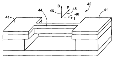
Nanomechanical devices, such as a doubly clamped
beam 42 illustrated in Fig. 4, are excited according to
an exemplary embodiment with a magnetomotive technique.
When an AC current 40 is driven through an electrode 44
atop doubly-clamped beam 42 in the presence of a
perpendicular magnetic field 46, a resultant Lorentz
force 48 causes beam 42 to move in a direction
perpendicular to both current 40 and field 46. As beam
42 oscillates, it sweeps through a given area of magnetic
-13-
CA 02568140 2006-11-23
WO 2006/076037 PCT/US2005/018490
flux, which generates an EMF (electromotive force)
proportional to the velocity of motion through field 46.
This EMF produces a voltage on contact pads 41 securing
beam 42. With harmonic motion, this velocity is
proportional to the displacement amplitude of beam 42.
Sweeping through frequencies for AC current 40 yields the
distinct Lorentzian peak of a damped, driven harmonic
oscillator, illustrated in Fig. 5. The center of the
peak in Fig. 5 is the resonance frequency of the bridge.
The full width at half maximum (FWHM) of the peak
determines the quality factor, or Q of the device.
When the driving force provided by AC current 40 is
sufficiently strong, the response of beam 42 deviates
from the traditional linear Lorentzian response
illustrated in Fig. 5 and instead assumes the distinctive
shape of a nonlinear oscillator. Fig. 6 illustrates
several nonlinear responses that become less linear with
increased amplitude. The nonlinear response is also
characterized by a hysteresis loop observed by sweeping
forward and backwards through the frequencies around the
resonance frequency.
Referring for a moment to Fig. 8, a hysteretic
frequency response for beam 42 driven by a sufficiently
strong AC current 40 to produce nonlinear behavior is
illustrated. Within a range of frequencies defined by
the boundaries of a hysteretic region 80, oscillating
beam 42 can occupy one of two dynamic bistable states
distinguished by their respective velocities or
amplitudes. By driving beam 42 at a single frequency
within hysteresis region 80, beam 42 can be manipulated
into two bistable states through the addition of a
modulation signal.
-14-
CA 02568140 2006-11-23
WO 2006/076037 PCT/US2005/018490
Fig. 10 depicts a change that occurs to the double-
well beam potential with the addition of a modulation
signal. The potential is biased in one direction or
another by the modulation, forcing the beam into one or
the other state. In this way it is possible to control
the state of the device through application of a
modulation.
As beam 42 is driven beyond a linear region, the
potential describing the restoring force of the
oscillator also changes. With drive amplitudes that
produce a linear response, the beam potential is the
classic quadratic shape of a linear harmonic oscillator.
This shape is illustrated as plot 72 in the graph of Fig.
7. As drive amplitude increases, the shape of the beam
potential evolves into a quartic shape, illustrated in
plot 74. Further amplitude increases produce a double-
well shape, illustrated in plot 76. Plot 76 indicates
operation of the beam as a nonlinear resonator.
Referring for a moment to Fig. 11, a schematic
diagram 110 of a circuit used to magneto-motively excite
a single doubly-clamped bridge structure into nonlinear
response and institute a read/write sequence through the
addition of a modulation signal is illustrated. An RF
source 112 provides an AC signal for exciting the bridge
structure, with modulation provided from modulator 114.
An RF lock-in 116 serves to monitor a voltage signal from
the element as passed through an amplifier 111. A
multimeter 118 measures the voltage signal to determine
the occupied amplitude state of the element.
Referring momentarily to Fig. 12, a typical
read/write sequence for a single nanomechanical memory
element is shown. The modulation signal in graph 122 is
a square wave, and the response of the element in graph
-15-
CA 02568140 2006-11-23
WO 2006/076037 PCT/US2005/018490
124 is the voltage reading from the RF lock-in described
in Fig. 11. The voltage difference between the two
amplitude states is approximately 2 uV, after factoring
out amplification, in this exemplary embodiment.
Referring to Fig. 13, a series of graphs 131 - 134
illustrate progressive increases in modulation amplitude.
At small modulation amplitudes, the beam experiences a
loss in fidelity, which reflects the presence of a
threshold amplitude appropriate for reproducible and
controllable switching.
Referring to Fig. 14, stability of the device over
relatively long periods is illustrated in graphs 142,
144. In this exemplary embodiment, the modulation and RF
driving signals are of sufficient amplitude to avoid the
need to refresh the memory element. As illustrated in
graphs 142, 144, the memory elements are stable
throughout time intervals on the order of hundreds of
seconds. Accordingly, the memory elements of the present
invention are comparable to SRAM, which need not be
refreshed, as opposed to DRAM, which is refreshed
constantly.
Due to the intrinsic dependence of the frequency of
an individual element on its dimensions, the mechanical
elements operated in accordance with the present
invention possess the distinct advantage that a reduction
in size naturally leads to an increase in the speed of
the device. That is, higher packing densities and faster
speeds are implied results of reduced size device.
Moreover, it is possible to fabricate many elements in
close proximity to each other with standard lithographic
techniques. Although the critical dimensions are sub-
micron, conventional semiconductor fabrication techniques
may be used to produce the nanomechanical elements.
-16-
CA 02568140 2006-11-23
WO 2006/076037 PCT/US2005/018490
Indeed, standard photolithography or nanoimprint
lithography are sufficient to create nanomechanical
memory arrays with read/write access times as fast as 500
MHz, for example. Elements can be formed to be nearly
identical with each other, leading to nearly identical
resonance frequencies. Tolerances in the fabrication
process lead to natural variations in the resonance
frequencies of the elements, however it is possible to
compensate for these differences. Alternately, or in
addition, an element array can be formed that consists of
several non-identical elements located at a single
address, as illustrated in Fig. 3. The different memory
elements distinguished by their different dimensions
permits them to be separately accessed due to their
unique resonances.
Other stimulation techniques besides magnetomotive
are available for operating the nanomechanical memory
elements. Although the magnetomotive technique described
above is advantageous for its simplicity and sensitivity,
it uses large magnetic fields, typically created with
superconducting solenoid magnets held at liquid helium
temperatures of about 4 Kelvin. Although it is possible
to place a sample within a room-temperature vacuum cell
at the center of such a magnet, the magnet itself implies
a low-temperature technique. In addition, the magnetic
fields are often in the range of several Tesla (T), which
is not a practically viable option for a realistic
implementation.
However, other techniques are available for room
temperature, magnetic-field free operation of the
nanomechanical memory devices according to the present
invention. There are no significant changes in the
dynamics, physics, or method of operation of these memory
-17-
CA 02568140 2006-11-23
WO 2006/076037 PCT/US2005/018490
elements for application of these other techniques. The
other techniques include accessing and stimulating
micromechanical and nanomechanical memory devices through
capacitive, piezoelectric and/or optical methods.
A typical optical method involves shining a laser on
the mechanical device and setting up an interference
pattern that describes the motion. Although effective
for larger structures, optical techniques tend to break
down as the device size is reduced, due to the
limitations inherent in the spot size of the laser.
Capacitive techniques provide a number of advantages
for both excitation and detection of the motion of
nanomechanical elements, including being effective at
room temperature and in air. Capacitive techniques
typically operate on the principle of inducing motion via
the application of an AC signal to a gate that is
capacitively coupled to a grounded resonator. The
resulting motion can be detected either by observing the
subsequent changes in the voltage between the oscillator
and a second gate, or through the application of optical
methods. It is also possible to set up a differential
capacitive measurement by providing four gates, rather
than two.
Referring to Fig. 15, a capacitively coupled beam
152 is excited and read through gates 154, 156,
respectively. Gates 154, 156 are placed on either side
of beam 152 and, according to an exemplary embodiment,
driven with an RF signal for excitation and detection.
This drive and detection arrangement is illustrated in
Fig. 16. An RF drive signal with a signal modulation are
applied to gate 154, which induces motion through
capacitive coupling with grounded electrode 162 atop
oscillator element 164. The resulting motion generates a
-18-
CA 02568140 2006-11-23
WO 2006/076037 PCT/US2005/018490
voltage signal between grounded oscillator 162, 164, and
detection, or reading gate 156. The voltage signal is
monitored for changes in state of element 164 to derive a
bistable memory operation.
S Referring to Fig. 17, beam 152 is illustrated as
being suspended above the silicon substrate. According
to another exemplary embodiment, coupling electrodes 172,
174 may be located beneath the oscillator, or may be
vertically oriented rather than laterally.
Referring to Fig. 18, an array 180 of capacitively
coupled elements is illustrated. The elements in array
180 are addressed capacitively and are nearly identical
with each other.
Referring to Fig. 19, an exemplary realization of a
multi-element memory cell 190 is illustrated. An array
of individually addressed elements is coupled to
circuitry formed as an addresser A and a decoder D. The
elements are fabricated to have similar, or nearly
identical, resonance frequencies. An RF source 192
generates an RF signal that is modulated by modulator
194. The modulated signal is provided to addresser A,
upon which addresser A determines an element to which a
write operation is applied. Decoder D reads a state of a
given element, and passes a voltage signal to RF lock-in
196, which is referenced to RF source 192 through
modulator 194.
Referring to Fig. 20, it is also possible to
fabricate a device 202 out of a piezoelectric material
such as quartz, for example. Piezoelectric device 202
can be excited and read through piezoelectric excitation
and detection of the motion of the resonating device.
Two opposing contacts 204, 206 are used to apply an AC
voltage difference between the top and bottom of device
-19-
CA 02568140 2006-11-23
WO 2006/076037 PCT/US2005/018490
202. The voltage difference produces a strain through
piezoelectric forces to induce a voltage between a second
pair of top/bottom contacts 205, 207. The induced
voltage permits a read operation through contacts 205,
207. A voltage difference may be applied between any
top/bottom set of electrodes to induce a strain in device
202, resulting in a voltage signal read by the other
top/bottom set of electrodes. Figs. 21 and 22 are
perspective views illustrating an exemplary orientation
of electrode pairs.
Piezoelectric driven devices opens the present
invention to the application of a number of different
materials that may be used to fabricate devices according
to the present invention. Materials used to fabricate
capacitive or piezoelectric driven devices include but
are not limited to silicon beams fabricated from an SOI
wafer, silicon nitride (SiN), silicon carbide (SiC),
gallium arsenide (GaAs), gallium nitride (GaN), quartz,
and diamond. In addition, it is possible to fabricate
these structures out of pure metals, bimetallic strips,
or other heterogeneous material compositions such as
semiconductor/metal compositions, two or more different
semiconductor materials, and so forth. Each composition
possesses distinct advantages and disadvantages, and the
overall operation of the device remains consistent.
Forming doubly clamped beams according to the
present invention may be carried out using bimetals or
multiple layer materials. In accordance with the present
invention, a device with a built-in compressive strain is
fabricated that exhibits inherent nonlinear behavior.
The nonlinear device can be driven without the use of
relatively large driving forces described previously.
Indeed, any driving force, no matter how small, applied
-20-
CA 02568140 2006-11-23
WO 2006/076037 PCT/US2005/018490
to the nonlinear device results in a nonlinear response
as a function of frequency. The relatively small driving
force applied to the nonlinear device generates dynamic
bistability through the creation and detection of
S distinct amplitude states. Accordingly, the driving AC
force and modulation can be significantly reduced,
resulting in significant power requirement reductions for
these devices.
According to another embodiment of the present
invention, a multi-stable mechanical memory device is
provided that exhibits more then two distinct stable
amplitude states. In one embodiment, the mufti-stable
device is formed with a higher degree of non-linearity
than the bistable devices discussed above. The formation
of the device includes the introduction of additional
compressive strain to increase the non-linearity of the
device. In another embodiment, additional non-linearity
is introduced into the device through stronger or higher
amplitude driving forces, leading to additional states in
the driven device. Memory devices with three or more
distinct states in accordance with the present invention
permit higher density information storage and
manipulation. The higher density of information leads to
greater efficiency across entire applications at all
levels, producing significant savings in space and power.
In addition, while planar devices have been
illustrated herein, the same devices may be constructed
to have a vertical, or out-of-plane orientation.
Accordingly, combination of memory elements in different
orientations can be provided to further improve
information density in a given application. For example,
the present invention contemplates the formation and use
-21-
CA 02568140 2006-11-23
WO 2006/076037 PCT/US2005/018490
of three-dimensional memory elements or blocks of
elements.
The nanomechanical memory elements discussed herein
can be formed to have critical dimensions in the range of
from about 10 to about 500 nm. The utilization of a
block-copolymer fabrication method may be able to realize
vertical-column structures with critical dimensions below
nm. These dimensions offer performance advantages in
speed and packing density comparable to present industry
10 standards. In addition, the elements of the present
invention are reliably operated in a manner distinct from
that of any other memory system.
Aside from the basic doubly-clamped beam or singly
clamped cantilever, the present invention contemplates a
number of realizations of a memory element based on
dynamic states. In addition to the flexural modes
described earlier, it is possible to observe and
manipulate dynamic multi-stable states in torsional or
shear modes. Alternative device geometry may be used to
realized the present invention, including paddle-type
devices, diaphragms, or vertical rods. Device geometries
may also include combinations of beams, cantilevers, or
diaphragms, for example, in which the motions of the
different sub-elements, either jointly or severally,
create the different states of the memory cell. For
example, relative or differential motion based on a
number of sub-elements may be used to realize the memory
element of the present invention.
According to another exemplary embodiment of the
present invention, the addition of a suitable DC bias
induces a frequency shift on a doubly-clamped beam
structure without forcing the structure into nonlinear
behavior. That is, fundamental or higher-order
-22-
CA 02568140 2006-11-23
WO 2006/076037 PCT/US2005/018490
frequencies of a beam in a linear response mode can be
controllably and reproducibly shifted between one or more
different frequency values through the application of a
DC bias signal. The modulation signal has a similar form
to that of the nonlinear case, but the "1" and "0" states
are frequency-dependent dynamic states, rather . than
nonlinear amplitude states. That is, in contrast to
differentiating between two voltages at a single
frequency, the circuit uses two frequencies with the same
or similar voltage responses to provide an element with
one or more dynamic states. Multiple states for the
element are provided through the application of one or
more DC biases to the element to achieve distinct
frequencies in distinct states. An illustration of
frequency dependent states that are produced through the
application of a DC bias is provided in the graph of Fig.
23. Fig. 23 shows the distinct frequency dependent
states of an element subjected to various DC biases. The
distinct frequencies may have a tolerance sufficient to
permit easy recognition of the separate states, based,
for example on a DC bias step of 1 Volt, as illustrated
in Fig. 23.
A practical realization of the nanomechanical memory
elements described according to the present invention
need not be limited to a solely mechanical device. For
example, the present invention contemplates hybrid
devices, consisting of mechanical and electrical or
electro-capacitive elements to form a memory cell. That
is, for example, distinct variations in capacitance may
be used as the operative dynamic states for the memory
cell, which may be achieved using mechanical or
electrical drives or operations. In addition, an overall
read/write circuit may use the hybrid devices to take
-23-
CA 02568140 2006-11-23
WO 2006/076037 PCT/US2005/018490
advantage of conventional or unique electronic,
mechanical, or hybrid input/output protocols.
Finally, it will be appreciated that modifications
to and variations of the above-described apparatus and
method may be made without departing from the inventive
concepts disclosed herein. Accordingly, the invention
should not be viewed as limited except by the scope and
spirit of the appended claims.
-24-