Note: Descriptions are shown in the official language in which they were submitted.
CA 02568260 2006-11-15
File number : 1 1 1 75-001
Revision : As Filed
Date : 2006/11/15
Title of the Invention
[0001 ] Transparent Material Inspection System.
Cross-Reference to Related Applications
[0002] There are no cross-related applications.
Field of the Invention
[0003] This invention relates systems and apparatuses for the inspection of
transparent
materials such as, but not limited to, lens, eyewear, visors and eyewear
shields. More
particularly, the present invention relates to systems and apparatuses for the
inspection of
transparent materials which use charged coupled device (CCD) or similar
cameras.
Background of the Invention
[0004] The testing of transparent material, such as contact lenses and
eyewear, for optical
properties, quality, colour, flaws and defects has previously been mainly
performed by
human inspectors who had to manually verify each object. Such a technique is
generally
prone to human error, lacks uniformity, and furthermore, is particularly
tedious. Indeed,
the quality of consecutive inspections can vary according to the degree of
tiredness of the
inspector.
[0005] Thus, in order to mitigate the lack of uniformity of transparent
material
inspection, some automated systems have been developed over the years for
inspecting
transparent materials.
[0006] Yet, since the objects which were usually most tested were
ophthalmologic or
contact lenses, the automated inspection systems which have been proposed over
the
years were generally specifically designed for such lenses. For example,
Lafferty et al.
-1-
CA 02568260 2006-11-15
File number : 11175-001
Revision : As Filed
Date : 2006/11/15
(U.S. Patent Nos. 5,801,822 and 5,818,573) proposed a system for inspecting
ophthalmic
lenses using either light emitting diodes (LED) or optical fibers and light
diffuser. The
defects in the lenses were detected via a CCD camera located on the other side
of the
lenses. The system of Lafferty et al. could also be provided with multiple
light sources
and hence, multiple cameras.
[0007] More recently, another lenses inspection system was proposed by
Nishikawa
(U.S. Patent No. 6,373,578). In this system, which is particularly designed
for inspecting
lenses used in recording device (e.g. compact disk writer), the lens is
inspected via a laser
and an interferometer. Understandably, the system is quite limited to specific
types of
lenses.
[0008] A more general system for the detection of transparent and/or light
diverting
defects in transparent material was proposed by Weiss et al. (U.S. Patent No.
6,633,377).
The system of Weiss et al. uses dark views to detect to presence of light
diverting defects.
[0009] Yet, even though all these systems are generally useful for their
intended
purposes, they are all generally limited in their applications. First, they
are generally
adapted for specific types of objects such as ophthalmic lenses which prevents
the use of
the same equipment for inspecting other types of transparent material.
Moreover, prior art
inspecting systems are generally not adapted to measure optical properties
while also
detecting flaws and defects. Finally, prior art inspecting systems generally
use
monochromatic light. Hence, defects which are generally non apparent when
viewed in
monochromatic light cannot be detected.
[0010] There is thus a need for a novel transparent material inspection system
which
generally obviates to aforementioned drawbacks.
Summary of the Invention
-2-
CA 02568260 2006-11-15
File number : 11175-001
Revision : As Filed
Date : 2006/11/15
[0011 ] In accordance with the present invention, there is provided a novel
system for the
inspection of transparent materials such as, but not limited to, contact
lenses, protective
glasses, display glass panels, eyewear shields, visors, etc.
[0012] Generally speaking, the inspection system of the present invention
comprises a
liquid crystal display (LCD) or similar screen which emits variable and
preferably
preprogrammed patterns of light through the transparent part under inspection.
The image
of the pattern through the inspected transparent part is then captured by a
charged
coupled device (CCD) or similar camera. The camera then transmits the data to
an image
processing module which then transmits the processed image to an analysis
module. The
lattel- generally measures, when applicable, the dimensions of the part, its
transparency,
its colour and its optical strength. Understandably, depending on the
capabilities of the
analysis module, other optical properties could also be determined and/or
measured. The
analysis module also advantageously detects the presence of dots, stains,
scratches,
optical distortions, fingerprints, cloudiness and other optical artefacts
and/or defects in
the transparent material. The patterns emitted by the LCD screen are
preferably designed
to measure the optical specifications and also to highlight potential defects.
[0013] Accordingly, the present invention preferably comprises a LCD connected
to a
LCD panel driver. Still, other systems to display images could also be used if
found to
work adequately in the context of the present invention. Accordingly, the
expression
LCD must not be narrowly construed and should be interpreted as encompassing
other
similar display systems having generally similar capabilities.
[0014] The system further comprises a CCD camera which is connected to an
image
processing module. As for the LCD, the CCD camera should not be narrowly
construed
and should be interpreted as encompassing other image capturing systems having
generally similar capabilities.
[0015] The LCD panel driver and the image processing module are further
connected
together via a computer system which is preferably provided with a user
interface for
-3-
CA 02568260 2006-11-15
File nuniber : 1 1 1 75-00 1
Revision : As Filed
Date : 2006/11/15
generally allowing a human operator to monitor the inspection process. Yet,
the LCD and
the CCD are preferably located inside a dark room or enclosure, substantially
sealed from
exterior light, in order to prevent such exterior light to interfere with the
inspection
process.
[0016] In order to inspect an object comprising a portion made of transparent
material,
the object is placed between the LCD and the CCD in order for the camera to be
able to
capture the image of the pattern projected by the LCD after its passage
through the
transparent material. The image captured by the CCD is then sent to the image
processing
module for image processing and then to an analysis module for further optical
properties
analysis and defect analysis.
[0017] Depending on the level of inspection needed for particular objects, the
analysis
module is generally adapted to measure at least certain optical properties of
the
transparent material. For example, in the case of a lens, the analysis module
would
generally be adapted to measure its dimensions, its transparency and its
optical strength.
Furthermore, in the particular case of tinted lens (e.g. sunglass lens), the
analysis module
would also be preferably able to measure the colour of the lens. Yet, in the
case of glass
panels used, for example, in the manufacture of cathode ray tube (CRT)
monitors and
LCD screens, the optical properties analysis of the analysis module could be
limited to
fewer optical characteristics.
[0018] Advantageously, the optical properties to be determined and/or measured
could be
chosen by a human operator via the user interface. Also, preprogrammed optical
properties analyses for specific objects could be stored on the computer
system. These
preprogrammed analyses could be loaded prior to the inspection of certain
objects. The
present inspection system is therefore able to inspect transparent objects and
materials of
different size and shape.
[0019] Still, an important aspect of the present system is the detection of
defects in the
transparent material. Indeed, in order for the inspection system to be able to
detect
-4-
CA 02568260 2006-11-15
File nnniber : 11175-001
Revision : As Filed
Date : 2006/11/15
different types of defects, the LCD, via the LCD panel driver and the computer
system, is
able to project different light patterns, each of which can be used to
highlight particular
defects. Preferably and to speed up the inspection process, the patterns are
generally and
preferably preprogrammed and projected in a consecutive manner. Still, it
could be
possible to manually select certain patterns via the user interface in order,
for example, to
inspect more closely certain defects. Moreover, it is also possible to create
new or custom
patterns and to load them into the computer system.
[0020] The inspection system, according to the present invention, will
generally detect
scratches, dots, bubbles, fingerprints, distortion, stains and other similar
defects.
[0021] Accordingly, the system of the present invention generally works by
projecting a
first pattern which image through the transparent material is captured by the
CCD and
processed and analysed by the image processing module and by the analysis
module
respectively. Then a second pattern is projected and its image through the
transparent
material is captured by the CCD and similarly processed and analysed by the
image
processing module and the analysis module. The process continues as long as
there are
patterns to be displayed. In a possible alternative embodiment, the projection
of patterns
could be stopped by the detection of a major and generally fatal defect.
[0022] According to an aspect of the present invention, the inspection system
is provided
with a coordinates calibration procedure. The object of this procedure is
generally to
match the pixel coordinates of the LCD with the sensor coordinates of the CCD.
[0023] Also, according to an important aspect of the present invention, the
inspection
system is also provided with an intensity calibration procedure. This
procedure calibrates
the intensity of each pixel of the LCD so that the captured image of the LCD
on the CCD
is of uniform intensity. Since the position of each pixel on the LCD must
generally be
precisely known in order to correctly adjust its intensity, this second
calibration
procedure is generally executed after the coordinates calibration procedure.
These
calibration procedures are generally iterative in nature.
-5-
CA 02568260 2006-11-15
File number : 11175-00 (
Revision : As Filed
Date : 2006/11/15
[0024] By calibrating the intensity of the pixels of the LCD prior to the
inspection
procedure, the present invention is generally able to detect more defects
since the image
effectively captured by the CCD is substantially not biased by variation in
the intensity of
the pixels of the LCD.
[0025] The features of the present invention which are believed to be novel
are set forth
with particularity in the appended claims.
Brief Description of the Drawings
[0026] The above and other objects, features and advantages of the invention
will
become more readily apparent from the following description, reference being
made to
the accompanying drawing in which:
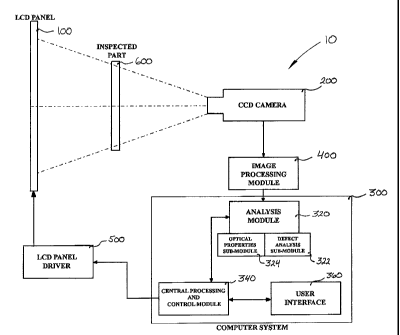
[0027] Figure 1 is a schematic view of an embodiment of the inspection system
of the
present invention.
Detailed Description of the Preferred Embodiment
[0028] A novel system for inspecting transparent material will be described
hereinafter.
Although the invention is described in terms of specific illustrative
embodiments, it is to
be understood that the embodiments described herein are by way of example only
and
that the scope of the invention is not intended to be limited thereby.
[0029] Referring now to Fig. 1, the inspection system 10 of the present
invention
generally comprises a LCD panel 100 and a CCD camera 200 facing the LCD. The
alignment between the LCD 100 and the CCD 200 can be chosen and changed as
required according to any type of inspection.
-6-
CA 02568260 2006-11-15
File number : 1 1 1 75-001
Revision : As Filed
Date : 2006/11 / 15
[0030] The LCD panel 100 is in electronic communication, with wire or
wirelessly, with
a LCD panel driver 500. Understandably, the LCD panel driver 500 controls the
LCD
panel 100 and the images projected thereby. Preferably, the LCD panel driver
500 is able
to control the intensity of each individual pixel forming the LCD panel 100.
[0031] The CCD camera 200 is in electronic communication, with wire or
wirelessly,
with an image processing module 400. The image processing module 400 generally
comprises all the hardware such as processors and storage devices and the
softwares such
as databases and image processing softwares to adequately process, store
and/or retrieve
the images captured by the CCD 200. The image processing module 400 could also
be
provided with additional hardware and/or additional softwares if necessary.
[0032] In order to close the loop, the image processing module 400 and the LCD
panel
driver 500 are further connected together via a computer system 300.
Understandably, the
connection therebetween could be with wire or wireless.
[0033] As can be seen from Fig. 1, the computer system 300 itself comprises
several
modules. First, the computer system 300 comprises a central processing and
control
module 340 which is in electronic communication with the LCD panel driver 500.
The
computer system 300 also comprises an analysis module 320, itself comprising a
defect
analysis sub-module 322 and an optical properties analysis sub-module 324. The
analysis
module 320 is electronically connected with the image processing module 400.
Finally,
the computer system 300 preferably comprises a user interface 360, generally
in the form
a display screen coupled with input means such as a keyboard (not shown)
and/or a
pointer device (not shown). Other user interface could also be used.
[0034] As shown in Fig. 1, the analysis module 320 and the user interface 360
are
generally connected to the central processing and control module 340.
-7-
CA 02568260 2006-11-15
File number : 11175-001
Revision : As Filed
Date : 2006/11 / 15
[0035] Though not shown for clarity, it is to be understood that the LCD 100
and the
CCD 200 are preferably mounted inside a dark room or enclosure to prevent
exterior light
from interfering with the inspection procedure.
[0036] Prior to inspecting transparent material, the system 10 of the present
invention is
preferably calibrated in order to adjust the coordinates system between the
LCD 100 and
the CCD 200 and also to adjust the intensity of the LCD 100 with respect to
the
receptivity of the CCD 200. Such calibration procedures shall be further
described
hereinbelow. In any case, the system 10 of the present invention is not
limited to any
particular calibration methods.
[0037] In use, an object, part or product, comprising a portion made of
transparent
material 600 to be inspected, is placed between the LCD 100 and the CCD 200.
Then,
the LCD 100, driven by the computer system 300 via the LCD panel driver 500,
projects
a series of preferably preprogrammed light patterns through the transparent
material 600,
the images of which are then captured by the CCD 200. The captured images are
then
processed by the image processing module 400 and then preferably sent to the
analysis
module 320 of the computer system 300 for further analyses.
[0038] Depending on the type of inspection required, when the captured images
are in the
analysis module 320, they can be analysed for defect detection by the defect
analysis sub-
module 322 and/or they can be analysed for optical properties determination
and
measurement by the optical properties analysis sub-module 324.
[0039] As the captured images of the projected patterns are analysed, an
indication of the
progress of the inspection process can be displayed on the user interface 360.
At the end
of the inspection process, a report can be advantageously displayed on the
user interface
360. Such a report would preferably contain the relevant information
concerning the
measured optical properties and the detected defects if any.
-8-
CA 02568260 2006-11-15
File number : 1 1 1 75-001
Revision : As Filed
Date : 2006/11/15
[0040] Understandably, should the object, part or product comprising
transparent
material 600 to be inspected be curved and/or of large size, the system 10 of
the present
invention could be provided with multiple LCD 100 and correspondingly multiple
CCD
200 to fully cover the object, part or product.
[0041] One of the main advantages of the present invention is the ability of
the LCD 100
to project patterns of different types and configurations, each pattern being
generally
adapted to highlight certain defects or to measure particular optical
properties. However,
in order to fully use the capacity of the LCD 100, the inspection system 10 of
the present
invention and more particularly its computer system 300, is provided with
methods or
procedures to calibrate the coordinates and the intensity of the pixels of the
LCD with
respect to the images captured by the CCD.
[0042] First, concerning the coordinates, to precisely inspect transparent
material, the
position and orientation of the pattems projected by the LCD 100 must be
precisely
known. Also, unless a telecentric lens is used on the CCD camera 200, which is
not
always possible due to the size of the inspected parts, the projected patterns
will generally
be at least slightly deformed. Therefore, the coordinates calibration
procedure is used to
enable the projection of the patterns at the desired coordinates and to modify
their shape
to compensate the deformation due to the lens of the CCD 200.
[0043] Therefore, prior to inspecting transparent material 600, the system 10
preferably
calibrates the coordinates of the pixels of the LCD 100 with the coordinates
of the CCD
200. In one exemplary though not limitative version of the procedure, the
computer
system 300 instructs the LCD 100, via the LCD panel driver 500, to project a
pattern of
rows and columns of dots. These dots have known positions. Then the image of
this
pattern is captured by the CCD 200 and processed by the image processing
module 400.
The processed image is then sent to the computer system 300 in order for the
computer
system 300 to determine the positions of the dots on the captured image of the
pattern.
The computer system 300 then compares the positions of the projected dots with
the
measured positions of the dots on the captured image of the pattern and then
computes
-9-
CA 02568260 2006-11-15
File number : 1 1 1 75-001
Revision : As Filed
Date : 2006/11/15
the difference therebetween. Using the aforementioned computed difference, the
computer system generates a modified pattern which is then projected by the
LCD 100
and captured by the CCD 200. The process recited above is then repeated
iteratively until
the expected positions of the projected dots and their measured positions are
the same.
[0044] According to the preferred embodiment, this calibration of the
coordinates is
generally crucial to the next calibration, the intensity calibration.
[0045] As it is generally known in the art, LCD panels are composed of a
plurality of
pixels, each of which is capable of producing the range of colour for which
the LCD was
designed. Yet, despite quality control in the manufacturing process, it
remains possible
that two pixels located on the same LCD and equally electrically excited
produce the
same colour but with a slight difference in intensity. Moreover, the intensity
of the pixels
can change over time as the LCD becomes older. Finally, and more importantly,
the
angle from which a pixel is viewed will affect the perceived intensity
thereof.
[0046] On the CCD 200 side, it is generally known that lens located therein
may affect
the captured intensity of certain pixels of the LCD.
[0047] Thus, for example, even though it might not be visible to the naked
eye, it is fairly
possible that a completely white LCD screen may not effectively be of equal
intensity
and/or that the captured image of a completely white LCD screen may not be
seen as
being evenly white and/or as having an even intensity.
[0048] Thus, to equalise what is effectively captured and perceived by the CCD
200, and
which is effectively processed and analysed, the computer system 300
preferably
calibrates the LCD 100 prior to inspecting transparent material 600.
[0049] In one exemplary manner, the computer system 300 instructs the LCD 100,
via
the LCD panel driver 500, to project a pattern of even intensity. The pattern
is then
captured by the CCD 200 and processed by the image processing module 400 prior
to
-10-
CA 02568260 2006-11-15
File nuniber : 1 i 175-001
Revision : As Filed
Date : 2006/11/15
being sent to the computer system 300. The computer system 300 then compares
the
intensity of the pixels of the captured image of the pattern with the
intensity of the pixels
of the pattern effectively projected. The computer system 300 then computes
and applies
a multiplicative matrix to the projected pattern to compensate for the
difference between
the projected intensity and the captured one. The corrected pattern is then
projected by
the LCD 100 and the image is captured by the CCD 200. The captured image of
the
corrected pattern is then processed by the image processing module 400 and
sent to the
computed system for comparison with the projected pattern. The foregoing
process is
then repeated until the image captured by the CCD 200 is of even intensity.
[0050] It is to be understood that in order to compensate the right pixels,
their position
must be precisely known and that generally explains why the coordinates
calibration is
generally required prior to the intensity calibration. Moreover, the skilled
addressee will
understand that the pattern projected at the end of the intensity calibration
may be of
uneven intensity. However, the CCD 200 perceives this uneven intensity as
even.
[0051 ] It is also to be understood that the calibration procedures described
above are
executed without the present of transparent material 600 between the LCD 100
and the
CCD 200.
[0052] Once the calibrations are done, the inspection of transparent material
600 can
begin. Still, in order to maintain the quality of the inspection, the
inspection system 10
may be recalibrated as often as required.
[0053] While illustrative and presently preferred embodiments of the invention
have been
described in detail hereinabove, it is to be understood that the inventive
concepts may be
otherwise variously embodied and employed and that the appended claims are
intended to
be construed to include such variations except insofar as limited by the prior
art.
-11-