Note: Descriptions are shown in the official language in which they were submitted.
CA 02568422 2012-11-09
WIRELESS REPEATER IMPLEMENTING LOW-LEVEL OSCILLATION
DETECTION AND PROTECTION FOR A DUPLEX COMMUNICATION SYSTEM
TECHNICAL FIELD
The present invention relates to the field of duplex communication systems
such as the wireless telephone system, and more particularly to a wireless
repeater
for improving wireless telephone service within a building, such as a home or
office.
BACKGROUND OF THE INVENTION
Wireless telephone systems, which are a type of duplex or two-way
communication system, have become widely deployed throughout the United
States and abroad. In the United States, most service areas have a number of
competing types of wireless communication services for customers to choose
from.
These include the original analog system or Advanced Mobile Phone System
("AMPS") operating with a carrier frequency in the region of 800 MHz
("Cellular
band") as well as digital encoding protocols, uch as, Time-Division Multiple
Access ("TDMA"), Global System for Mobile communication ("GSM"), and Code-
Division Multiple Access ("CDMA"), which operate both in the Cellular band and
the
Personal Communication System ("PCS") frequency band region of 1900 MHz.
Wireless telephone service is also widely available using the European digital
1
CA 02568422 2006-11-27
WO 2005/119936 PCT/US2005/018611
systeffis operating in a carrier frequency band of 900 MHz ("GSM900") or the
1800
MHz Digital Communication System ("DCS") band using GSM encoding (and
GPRS/EDGE) and the 2100 MHz Universal Mobile Telephone System ("UMTS")
band using CDMA encoding.
All of these wireless telephone systems can suffer from a loss of service in
areas where the propagating communication signals are weak due to distance
from,
the Base Transceiver Station ("BTS" or "cell tower") and/or because the signal
is
blocked by structures or other obstructions. For large buildings and
terrestrial
features, such as hills and mountains, this problem is addressed by strategic
placement of cell towers, which at this point can be seen in a line of site
from
almost anywhere in the United States. But indoors, where the building blocks
the
propagating communication signals, it is impractical for the service provider
to
attempt to solve the problem in all buildings by deploying additional BTSs.
For
large buildings, it may be practical to locate a dedicated BTS antenna to
provide a
strong communication signal throughout much of the building, but not for most
,
homes and small offices.
In most homes and small offices, it is not feasible for the users to obtain a
dedicated BTS antenna. In this situation, it is not cost effective for the
service
provider to locate a BTS antenna or increase the transmission power to satisfy
individual customers with indoor reception problems. For example, when service
is
poor in certain locations within the customer premises, such as an office in
the ,
basement, there is no practical way to obtain a strong communication signal
from a
cell tower. As a result, wireless repeaters suitable for receiving, amplifying
and
retransmitting the wireless communication signal to a specific location, such
as an
office located in the basement of the customer premises, have been developed
and have met with a certain amount of commercial success.
In order to meet the widespread need for improved wireless coverage in
homes and small-offices, a wireless repeater must be cost-effective; simple to
use,
easy to install, and safe for the service provider's network. In order to
accomplish
these requirements, a wireless repeater must satisfy several challenges.
First, the
wireless repeater system should be universal to protocol and modulation;
therefore,
it must be able to handle communications for the AMPS, TDMA, CDMA and GSM
systems in a cost-effective manner in the appropriate frequency band
(Cellular,
PCS, GSM900, DCS, UMTS etc.). Second, the wireless repeater system has to be
2
CA 02568422 2006-11-27
WO 2005/119936 PCT/US2005/018611
relatiVely easy to install by the non-technical customer or professional
installation
must be widely available at a reasonable cost (typically less than half of the
equipment cost). Third, the sysfem must be able prevent interference with the
Cellular or PCS network, including positive feedback ("self-oscillations")
which
develops between the two antennas of the wireless repeater system. This type
of
self-oscillation, similar to that experienced in audio systems when the
microphone
is placed too close a speaker, can cause serious problems within the wireless
network, including reduced capacity, reduced effective coverage, and loss of
service to other licensed users. Also, if not checked, an oscillation within
the
wireless repeater system can lead to destruction of its circuitry. Fourth, the
system
should be able to handle communication signals from both relatively near base
stations (i.e., relatively strong signals) and relatively far base stations
(i.e., relatively
weak signals) without creating disruptive interference. Fifth, the system
should be
able to handle communication signals from both relatively near mobile stations
(i.e.,
relatively strong signals) and relatively far mobile stations (i.e.,
relatively weak .4
signals) without creating disruptive interference.
Accordingly, there is an ongoing need for a wireless repeater system that is
cost-effective for home-based and small office locations. There is a further
need
for a cost- effective wireless repeater system configured to meet the
presently
experienced needs for such a system, including the ability to handle the
several v,
different types of communication signals that are presently in use, to detect
and ,
prevent low-level self-oscillations, to be easy to install or easy to have
professionally installed, and to control power transmission from near and far
base
stations and from near and far mobile stations.
SUMMARY OF THE INVENTION
The present invention meets the needs 'described above in a modular
wireless repeater system that allows a customer to purchase a unit for his or
her
present type of wireless service, such as Cellular or PCS, and then add on
modules for additional types of service that the customer may desire in the
future.
That is, the wireless repeater may be deployed as a single multi-band module
for
handling multiple wireless communication frequency bands, or as separate
modules for each individual wireless communications frequency band which may
be piggy-backed together to meet changing customer needs in a backward
3
CA 02568422 2006-11-27
WO 2005/119936 PCT/US2005/018611
comp'atible manner. Customers generally appreciate this type of configuration
flexibility.
Generally described, the invention may be deployed as a wireless repeater
to rebroadcast the communication signals which are present outside a building
from surrounding BTSs in order to provide improved wireless communications
service inside the customer premises. The wireless repeater system includes:
1) a
bi-directional amplifier ("BDA" or "Base Unit"), 2) a tower-signal antenna
that is
typically mounted on the roof or in an attic for best propagation to and from
the
BTS antenna, 3) a coaxial cable to connect the signal antenna to the Base
Unit,
and 4) a base unit indoor antenna that is typically located where improved
service
is desired for best propagation to and from the user's wireless communication
device or cellphone. The embodied wireless repeater system can also
simultaneously handle two or more types of wireless communications systems
presently in use in the United States and be upgraded with a subsequent module
in
the event that a new frequency is authorized for use in the future. For all of
these
wireless communications systems, the wireless repeater system detects low-
level
self-oscillations by discriminating these spurious oscillations from valid
communication signals such as pulsed signals, full-duplex analog continuous
wave
signals, and CDMA signals and prevents these self-oscillations from
interfering with
the communication networks by reducing the BDA gain or removing power to the
amplifiers. The embodied wireless repeater system performs intelligent power
control, allowing it to function properly with near and far BTS antennas and
mobile
stations.
The wireless repeater may also include a proactive isolation management
circuit configured to periodically increase the uplink gain of the BDA to
attempt to
trigger a low-level oscillation, and, thereby, ensure that adequate isolation
exists to
avoid ultra low-level spurious positive feedback. In these wireless system,
the
pulsed signals are typically characteristic of TDMA and GSM signals, the full-
duplex analog signals are characteristic of AMPS signals, and the continuous
wave
signals with high-frequency amplitude modulated ("AM") content are
characteristic
of CDMA signals.
In a particular physical configuration, the wireless repeater includes a base
unit having an enclosure that houses the bi-directional amplifier, and which
is
configured in a location within the customer premises. The wireless repeater
also
4
CA 02568422 2006-11-27
WO 2005/119936 PCT/US2005/018611
includes a base unit antenna located proximate to, and typically attached to,
the
enclosure and configured for bi-directional communications with wireless
communication terminals, typically telephones, located within the poor
reception
area. The wireless repeater also includes a tower-signal antenna located at
the
customer premises remotely from the enclosure, typically in an attic or on the
roof,
that is configured for bi-directional communications with the wireless BTS. In
addition, the wireless repeater includes a communication link, such as a
coaxial
cable, connecting the tower-signal antenna to the enclosure whereby the tower-
signal antenna may be strategically located at the customer premises for
communication with the BTS while the base unit antenna may be strategically
located within the customer premises for communication with the wireless
communication terminals located in the poor reception area.
The base unit of the wireless repeater configured as described above may
also include an oscillation detection circuit configured to detect
oscillations caused
by feedback from the tower-signal antenna to the base unit antenna, and an
..;;
oscillation protection circuit configured to lower or eliminate a gain setting
associated with the bi-directional antenna in response to detected
oscillations
caused by feedback from the tower-signal antenna to the base unit antenna.
The oscillation detection function includes a pulse detection circuit or
algorithm, such as a peak to average circuit, configured to dikriminate
between a
self-oscillation caused by feedback from the tower-signal antenna to the base
unit
antenna and a pulsed communication characteristic of TDMA and GSM signals.
The oscillation detection function may also include a modulation frequency
threshold detection circuit, typically set below a frequency characteristic of
CDMA
signals, configured to discriminate between self-oscillations which do not
have
much high-frequency AM content and a valid communication signal which does
have significant high-frequency AM content.
The oscillation detection circuit may also include a full duplex detection
circuit configured to discriminate between oscillations caused by feedback
from the
tower-signal antenna to the base unit antenna and a full duplex communications
characteristic of wireless telephone communication signals. For example, the
full
duplex detection circuit may typically include a mixing circuit configured to
generate
and detect the difference frequency between the downlink signal and the uplink
signal. This difference signal occurs at a constant frequency for any valid
full
CA 02568422 2006-11-27
WO 2005/119936 PCT/US2005/018611
duple* channel pair and is characteristic of AMPS communication signals and
many CDMA communication signals.
In addition, the oscillation detection circuit may include an isolation
management circuit configured to periodically increase the uplink gain of the
BDA
to trigger oscillations caused by feedback from the tower-signal antenna to
the
base unit antenna in order to maintain the minimum isolation needed and
maximize
the coverage gain.
More specifically stated, the wireless repeater includes a base unit antenna,
a tower-signal antenna, a bi-directional amplifier, and an oscillation
detection and
protection circuit. The oscillation detection and protection circuit typically
includes
a pulse detection circuit configured to discriminate between oscillations
caused by
feedback from the tower-signal antenna to the base unit antenna and pulsed
communication signals. The oscillation detection and protection circuit also
typically includes a modulation frequency threshold detection circuit
configured to
discriminate between oscillations caused by feedback from the tower-signal
antenna to the base unit antenna and a communication signal comprising a
significant component occurring above a modulation frequency threshold not
.
associated with an oscillation. The oscillation detection and protection
circuit
further includes a full duplex detection circuit configured to discriminate
between
oscillations caused by feedback from the tower-signal antenna to the base unit
antenna and a full duplex communication characteristic of full duplex
communication signals. The oscillation detection and protection circuit
also
typically includes a logic circuit configured to detect oscillations occurring
above a
threshold level that has been distinguished from a pulsed signal by the pulse
detection circuit, distinguished from a full duplex signal by the full duplex
detection
circuit, and distinguished from communications occurring above a threshold
frequency by the modulation frequency threshold detection circuit. The
oscillation
detection and protection circuit also typically includes a gain reduction
circuit to
attempt to eliminate the oscillation and a shutdown circuit configured to
disconnect
power to at least one of the amplifiers in response to an oscillation detected
by the
logic circuit.
The oscillation detection and protection circuit may also include a
continuous wave detection circuit configured to detect a continuous wave
signal
component. And it may also include a gain management circuit configured to
6
CA 02568422 2006-11-27
WO 2005/119936 PCT/US2005/018611
periodically increase the uplink gain of the BDA to trigger the occurrence of
oscillations caused by feedback from the tower-signal antenna to the base unit
antenna. The pulse detection circuit may include a peak to average circuit,
and the
pulsed communication signals may be characteristic of TDMA and GSM signals.
In addition, the full duplex detection circuit may include a frequency
detection circuit configured to detect signal components having a significant
amplitude occurring in downlink and uplink communication channels. The
downlink
and uplink communication channels may be characteristic of AMPS and CDMA
signals.
Further, the full duplex detection circuit may include a mixing circuit
configured to combine uplink and downlink signals to create a mixed duplex
signal,
a filter configured to receive the mixed duplex signal and produce a filtered
mixed
duplex signal by band-pass filtering the mixed duplex signal, and a power
detection
circuit configured to determine a power level associated with the filtered
mixed
duplex signal.
The specific techniques and structures for implementing particular
embodiments of the wireless repeater system, and thereby accomplishing the
advantages described above, will become apparent from the following detailed
description of the embodiments and the appended drawings and claims.
BRIEF DESCRIPTION OF THE DRAWINGS
FIG. 1 is a conceptual diagram showing the operating environment for a
wireless repeater system.
FIG. 2 is a circuit block diagram of the base unit of a wireless repeater
system.
FIG. 3 is a circuit block diagram of an uplink circuit in the base unit of
FIG. 2.
FIG. 4 is a circuit block diagram of a CDMA detection circuit in the base unit
of FIG. 2.
FIG. 5 is a circuit block diagram of a mixer circuit in the base unit of FIG.
2.
FIG. 6 is a circuit block diagram of a downlink circuit in the base unit of
FIG.
2.
FIG. 7 is a circuit block diagram of a microprocessor circuit in the base unit
of FIG. 2.
FIG. 8 is a logic flow diagram for uplink control in a wireless repeater
system.
7
CA 02568422 2006-11-27
WO 2005/119936 PCT/US2005/018611
FIG. 9 is a logic flow diagram for oscillation detection in a wireless
repeater
system.
FIG. 10 is a logic flow diagram for uplink power control in a wireless
repeater
system.
FIG. 11 is a logic flow diagram for downlink power control in a wireless
repeater system.
FIG. 12 is a conceptual block diagram of a modular wireless repeater
system.
DETAILED DESCRIPTION OF THE EMBODIMENTS
In view of the foregoing, it will be appreciated that the present invention
provides significant improvements in wireless repeaters for home and small
business use. The modular wireless repeater is typically deployed with a roof-
mounted tower-signal antenna and a base unit with a base unit ,antenna located
within the building, with the tower-signal antenna connected to the base unit
by a
750 coaxial cable. The system allows a customer to purchase a unit for all of
the
wireless service providers in a given frequency band, such as PCS or Cellular,
and
then add on modules for additional service providers in other bands that the
customer may desire in the future. The system can also be expanded to
accommodate new frequency bands and data modulation techniques that may be
implemented in the future. For wireless repeaters, this system uniquely uses
750
coaxial cable for satellite television and can, therefore, be installed by any
satellite
television installer. The system also detects and prevents low-level
oscillations.
The wireless repeater also performs intelligent power control in the downlink
allowing it to function properly with near and far BTS antennas and in the
uplink
allowing it to function properly with near and far mobile users.
The wireless repeater is typically deployed with a roof-mounted tower-signal
antenna and a base unit with a base unit antenna located within the building,
with
the tower-signal antenna connected to the base unit by a 750 coaxial cable.
However, the tower-signal antenna 'could be located anywhere that receives
acceptable signal power from the wireless BTS antenna, the base unit may be
located anywhere that provides acceptable signal power to the area where
improved service is desired, and any type of communication link may be
employed
to connect the tower-signal antenna to the base unit. For example, the
communication link could use a different type of cable, a telephone line, the
house
8
CA 02568422 2006-11-27
WO 2005/119936 PCT/US2005/018611
power wiring, a wireless communication link or any other suitable type of
communication technique.
The preferred embodiment of the base unit is shown as analog circuit blocks
with a microcontroller, but could be implemented using any suitable type of
amplification, power control, and logic circuitry. Of course, the specific
circuit
configuration is merely illustrative, and could be replaced by any other
circuit
configuration that implements equivalent functionality.
Likewise, the specific
control algorithms can be replaced by other control algorithms that implement
equivalent functionality.
Turning now to the drawings, in which like numerals refer to like elements
throughout the several figures, FIG. 1 is a conceptual diagram showing the
operating environment for a wireless repeater system 12 installed to provide
improved wireless communication service within a customer premises 10, such as
a home or small business. The wireless repeater system 12 includes a base unit
14 with a base unit antenna 18, which is typically located inside the customer
premises 10, and a tower-signal antenna 16, which is typically mounted on the
roof
of the customer premises. The tower-signal antenna 16 is connected to the base
unit 14 by a cable 20, typically a readily available 750 of the type used for
most
satellite television systems. As will be explained in more detail later, the
wireless
repeater system 12 implements intelligent power control so that it can
automatically
adjust its transmission power to be appropriate for communiaating with a near
tower 24 and a far tower 26. Of course, the designation "tower" is meant as a
generic terms to include any type of base station antenna location, whether it
be a
stand-alone tower, a multi-function tower, pole, church bell tower, building
or any
other suitable location. The most common communication signals in the United
States are 824-849 MHz for Cellular uplink and 869-894 MHz for Cellular
downlink,
and 1 850-1 91 0 MHz for PCS uplink and 1 930-1 990 MHz for PCS downlink.
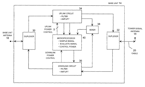
FIG. 2 is a circuit block diagram of the base unit 14 of wireless repeater
system 12. The base unit 14 engages in duplex communications with the tower-
signal antenna 16 and the base unit antenna 18. The communication signal from
the base unit antenna 18 is delivered to a duplexer 30; which separates uplink
and
downlink signals. The duplexer 30 delivers a signal to an uplink circuit 34
(FIG. 3)
that handles incoming uplink signals by filtering and amplifying the incoming
signals received from the duplexer 30. The uplink circuit 34 delivers an
o\utput
9
CA 02568422 2006-11-27
WO 2005/119936 PCT/US2005/018611
signal to a mixer 38 (FIG. 5), which combines the signal with another signal
from
the downlink circuit 36 and delivers the mixed signal to the microprocessor
40. The
uplink circuit 34 also delivers detected signals to the microprocessor 40 and
receives a 5-line uplink power control signal from the microprocessor 40 (FIG.
7).
The uplink circuit 34 also delivers its output communication signal to the
second
duplexer 32.
Simultaneously, the communication tower signal is sent from the tower-
signal antenna 16 via the 750 cable to the duplexer 32, which separates uplink
and
downlink signals. The duplexer 32 delivers a signal to a downlink circuit 36
(FIG. 6)
that handles incoming downlink signals by filtering and amplifying the
downlink
signals received from the duplexer 32. The downlink circuit 36 then delivers
an
output signal to the mixer 38 (FIG. 5), which combines the signal with another
signal from the uplink circuit 34. The downlink circuit 36 also delivers a
downlink
power detection signal to the microprocessor 40 (FIG. 7), and delivers its
output
communication signal to the duplexer 30.
FIG. 3 is a circuit block diagram of an uplink circuit 34. The signal received
from the duplexer 30 is received and amplified by an input amplifier 42. The
input
amplifier 42 sends its output signal to a band-pass filter 44, which passes
signals
about the range Of communication signal carrier frequencies used for the
applicable communications systems (e.g., Cellular or PCS, GSM900, DCS, etc). ,
The band-pass filter 44 sends its output signal to an uplink power control
amplifier =
(or attenuator) 46, which control the uplink power in response to control
signals
received from the microprocessor 40. The uplink power control amplifier 46
sends
its output signal to a crossover frequency notch filter 48, which ensures
adequate
isolation between the uplink and downlink amplifiers. The crossover frequency
notch filter 48 sends its output signal to a power .amplifier 50, which sends
its
output to a power coupler 52, which sends output power signals to the duplexer
32
and to a level adjuster (e.g. analog attenuator or amplifier) 54. The level
adjuster
54 sends its output signal to a power detector 56, which detects the power
amplitude envelope in the uplink frequency band. The power detector 56 sends
its
output signal to the microprocessor 40, which implements the oscillation
detection
and prevention algorithm along with power control.
The power detector 56 also sends an output signal to a CDMA detection
circuit 60, which passes high frequency content signal indicative of CDMA
CA 02568422 2006-11-27
WO 2005/119936 PCT/US2005/018611
comMunication signals to the microprocessor 40. The CDMA detection circuit 60
sends its output signal to the microprocessor 40, which implements the
oscillation
detection and prevention algorithm as noted above. Specifically, the
microprocessor 40 may send an uplink power control signal (e.g., 5-line
digital
control latch signal) to the power control amplifier 46 to trim the power in
the uplink
circuit. The microprocessor 40 may also send an uplink shut down signal to the
input amplifier 42 if the positive feedback oscillation cannot be adequately
controlled by the power control amplifier 46.
FIG. 4 is a circuit block diagram of the CDMA detection circuit 60. The
signal from the power amplitude detector 56 is received at an amplifier 62,
which
amplifies the signal and sends it to a high pass filter 64, which typically
passes
' signals above 50kHz. The high pass filter 64 sends its output signal to a
voltage
threshold detector 66, which sends its output signal to the microprocessor 40.
FIG. 5 is a circuit block diagram of the mixer circuit 58, which receives
input
signals from the uplink circuit 34 and the downlink circuit 36. These signals
are
amplified by amplifiers 72 and 74, respectively, and the resulting signals are
combined and sent to a band-pass filter that passes the duplex difference
signal
(e.g. 45 MHz for the Cellular band) to detect whether the signal is a duplex
communication signal or a spurious oscillation signal.
FIG. 6 is a circuit block diagram of the downlink circuit 36. The signal ,õ
received from the duplexer 30 is received and amplified by a downlink
amplifier 82.
The downlink amplifier 82 sends its output signal to a band-pass, filter 84,
which
passes signals about the range of communication signal carrier frequencies
used
for the applicable communications systems (e.g., Cellular, PCS, GSM900, DCS,
etc.). The band-pass filter 84 sends its output signal to a variable voltage
attenuator 86, which controls the downlink power in response to pulse-width
modulated control signals received from the microprocessor 40 via a low-pass
filter
96. The variable voltage attenuator 86 sends its output signal to band pass
filter
88, which passes the carrier frequencies for the applicable communications
systems (e.g., Cellular, PCS, GSM900, DCS, etc.). The band pass filter 88
sends
its output signal to an output power amplifier 90, and then on to a power
coupler
92, which sends output power signals to the duplexer 32 and to a power
detector
94, which detects whether an over power condition is present in the downlink
signal.
11
CA 02568422 2006-11-27
WO 2005/119936 PCT/US2005/018611
The power detector 94 sends its output signal to the microprocessor 40,
which implements the power control algorithm. Specifically, the microprocessor
40
may send a pulse-width modulated downlink power control signal to the variable
voltage attenuator 86 via the low-Pass filter 96. The microprocessor 40 may
also
send a downlink shut downlink power control amplifier 82 if the over power
condition cannot be adequately controlled by the variable voltage attenuator
86.
The specific microprocessor 40 circuit configuration is described in more
detail
below with reference to FIG. 7.
FIG. 7 is a circuit block diagram of the microprocessor circuit 40. The
microprocessor circuit includes a central processing unit (CPU) 92 that
operates in
accordance with a clock signal from the clock 92. The microprocessor circuit
40
also includes analog-to-digital processing units (A/D) 94a-d to convert the
analog
signals received from the analog circuit components into digital signals for
digital
processing within the CPU 92. The A/D 92a receives an analog signal from the .
uplink power detector 56 and sends a corresponding digital signal to the CPU
92.
The A/D 92b receives an analog signal from the CDMA detector 60 and sends a
corresponding digital signal to the CPU 92. The A/D 92c receives an analog
signal
from the mixer 38 and sends a corresponding digital signal to the CPU 92. The
A/D 92d receives an analog signal from the downlink power detector 94 and
sends
a corresponding digital signal to the CPU 92.
The central processing unit (CPU) 92 sends uplink power control signals to
the uplink power control amplifier 46. The central processing unit (CPU) 92
also
sends uplink power shut down signals to the uplink power control amplifier 42.
The
central processing unit (CPU), 92 sends pulse-width modulated downlink power
control signals to the variable voltage attenuator 86 via the low-pass filter
96. The
central processing unit (CPU) 92 also sends downlink power shut down signals
to
the downlink power control amplifier 82. The specific microprocessor 40
control
algorithm is described in more detail below with reference to FIGS. 8-11.
FIG. 8 is a logic flow diagram showing Routine 100 for detecting a small or
latent oscillation that may be indicative of an impending positive feedback
situation.
In step 102 (FIG. 9), the microprocessor 40 monitors the uplink signals to
detect an
oscillation that may be indicative of a positive feedback situation. Step 102
is
followed by step 104, in which the microprocessor 40 determines whether an
oscillation is present. If an oscillation is not present, the "NO" branch is
followed
12
CA 02568422 2006-11-27
WO 2005/119936
PCT/US2005/018611
'back .to step 102, and the microprocessor 40 continues to monitor the uplink
power. If an oscillation is present, the "YES" branch is followed to step 106,
in
which the microprocessor 40 determines whether the uplink attenuation is at
its
maximum value. If the uplink attenuation is NOT at its maximum value, the "NO"
branch is followed to step 108, in which the microprocessor 40 increments the
attenuation signal to the uplink power control amplifier 46 (FIG. 3) typically
by 6 dB.
The microprocessor 40 may loop through this control process several times to
implement stepped attenuation, for example using the 5-line latch signal to
sequentially increase the attenuation applied by the uplink power control
amplifier
46 from zero to 30 dB in 6 dB increments. Step 108 is followed by step 110, in
which the microprocessor 40 waits two minutes and then loops back to step 102,
and the microprocessor 40 continues to monitor the uplink power. If the uplink
attenuation is at its maximum value, the "YES" branch is followed from step
106 to
step 112, in which the in which the microprocessor 40 sends a shut down signal
to
the uplink input filter 42. Routine 200 then loops back to step 102 when the
base
unit is reset after the installer corrects the antenna isolation (separation).
FIG. 9 is a logic flow diagram for oscillation detection Routine 102 (i.e.,
step
102 in FIG. 8). In step 120, the microprocessor 40 determines whether a CDMA
signal has been detected by determining whether the uplink signal contains a
high
frequency component indicative of a CDMA signal. See FIG. 4. If a CDMA,signal
is detected, the microprocessor 40 deems that the uplink signal does not
contain a
positive feedback oscillation, and the "YES" branch is followed to stop 124
and
normal operation continues. If a CDMA signal is NOT detected, then the "NO" is
followed from step 120 to step '122, in which the microprocessor 40 determines
whether an analog duplex (e.g., AMPS) signal has been detected by determining
whether the uplink signal contains a difference signal indicative of analog
duplex
communications signals. See FIG. 5. If an analog duplex signal is detected,
the
microprocessor 40 deems that the uplink signal does not contain a positive
feedback oscillation, and the "YES" branch. is followed to stop 124 and normal
operation continues. If an analog duplex signal is NOT detected, then the "NO"
is
followed from step 122 to step 126, in which the microprocessor 40 determines
whether a pulsed signal indicative of TDMA encoded communication signals has
been detected by determining if a pulse of predetermined amplitude is present
in
the uplink signal. See FIG. 3, power detector 56. If a pulsed signal is
detected,
'13
CA 02568422 2006-11-27
WO 2005/119936 PCT/US2005/018611
the Microprocessor 40 deems that the uplink signal does not contain a positive
feedback oscillation, and the "YES" branch is followed to stop 124 and normal
operation continues. If a pulsed signal is NOT detected, then the "NO" is
followed
from step 122 to step 128, in which the microprocessor 40 deems that a
positive
feedback oscillation has been detected. In this case, the microprocessor 40
implements uplink (FIG. 8) and downlink (FIG. 10) power control.
FIG. 10 is a logic flow diagram showing Routine 200 for controlling the uplink
power in response to an over power situation (e.g., the mobile user device is
too
close to the base unit antenna). In step 202, the microprocessor 40 monitors
the
uplink signals to detect excessive power. Step 202 is folloWed by step 204, in
which the microprocessor 40 determines whether the uplink power is above a
predetermined threshold value. If the uplink power is above a predetermined
threshold value, the "NO" branch is followed back to step 202, and the
microprocessor 40 continues to monitor the uplink power. If an excess power is
present,,the "YES" branch is followed to step 206, in which the microprocessor
40 4
determines whether the uplink attenuation is at its maximum value. If the
uplink
attenuation is NOT at its maximum value, the "NO" branch is followed to step
108,
in which the microprocessor 40 increments the attenuation signal to the uplink
power control amplifier 46 (FIG. 3), typically by 1 dB. The microprocessor 40
may
loop through this control process several times to implement stepped
attenuation,
for example using the 5-line latch signal to sequentially increase the
attenuation
applied by the uplink power control amplifier 46 from zero to 30 dB in 1 dB
increments. After step 208, the microprocessor 40 loops back to step 202 and
the
microprocessor 40 continues to monitor the uplink power. If the uplink
attenuation
is at its maximum value, the "YES" branch is followed from step 206 to step
210, in
which the microprocessor 40 sends a shut down signal to the uplink input
filter 42.
Routine 200 then waits 10 seconds and then loops back to step 202 when the
base
unit is reset.
FIG. 11 is a logic flow diagram showing Routine 300 for controlling the
downlink power in response to an over power situation. In step 302, the
microprocessor 40 monitors the downlink signals to detect excess power that
may
be indicative of a very near BTS antenna. Step 302 is followed by step 304, in
which the microprocessor 40 determines the downlink power is above a
predetermined threshold value. If the downlink power is above a predetermined
14
CA 02568422 2006-11-27
WO 2005/119936 PCT/US2005/018611
threshold value, the "NO" branch is followed back to step 302, and the
microprocessor 40 continues to monitor the downlink power. If excess power is
present, the "YES" branch is followed to step 306, in which the microprocessor
40
determines whether the downlink attenuation is at its maximum value. If the
downlink attenuation is NOT at its maximum value, the "NO" branch is followed
to
step 308, in which the microprocessor 40 increments the attenuation signal to
the
variable voltage attenuator 86 (FIG. 6), typically by 1 dB. Step 308 is
followed by
step 310, in which the microprocessor 40 also increments the attenuation
signal to
the uplink power control amplifier 46 (FIG. 3), typically by 1 dB in order to
keep the
communication link balanced. The microprocessor 40 may loop through this
control process several times to implement stepped attenuation, for example
using
a pulse-width modulation to sequentially increase the attenuation applied by
the
downlink variable voltage attenuator 86, and using the 5-line latch signal to
sequentially increase the attenuation applied by the uplink power control
amplifier
46, the step the uplink and downlink attenuation from zero to 20 dB in 1 dB ,
increments. After step 310 the microprocessor 40 loops back to step 302 and
the
microprocessor 40 continues to monitor the downlink power. If the downlink
attenuation is at its maximum value, the "YES" branch is followed from step
306 to ,
step 312, in which the microprocessor 40 sends a shut down signal to the
downlink
amplifier 42. Routine 300 then waits two minutes and then loops back to step
302
when the base unit is reset.
FIG. 12 is a conceptual block diagram of a modular wireless repeater
system that includes a dual-band tower-signal antenna 400 connected to an
upgradable base unit 404 by way of a 750 coaxial cable 402. The upgradable
base unit 404, which includes a Cellular system (e.g., 800 MHz) base unit
antenna
406, is configured to implement wireless repeater functions for a Cellular
band
system. The upgradable base unit 404 includes a diplexer 407 to split Cellular
signals from PCS signals and a switch 420 to activate pass-through
connectivity to
an output port for PCS signals. An add-on PCS base unit 414 with a PCS base
unit antenna 416 may be connected to the output port of the upgradable base
unit
404 to receive the PCS band signals passed through the upgradable base unit.
Again, the cables 402 are standard 750 coaxial cables, and the ports on the
upgradable base unit 404 and the add-on base unit 414 are also standard for
750
coaxial cable. Of course, the upgradable base unit 404 could be operative for
PCS
CA 02568422 2006-11-27
WO 2005/119936 PCT/US2005/018611
systerh signals, or signals for any other wireless communication system.
Similarly,
the add-on base unit may be operative for Cellular system signals, or signals
for
any other wireless communication system. In addition, any number of add-on
base
units may be piggy-backed together to create a modular wireless repeater that
may
be augmented to meet the customer's needs as they change over time.
16