Note: Descriptions are shown in the official language in which they were submitted.
CA 02568966 2007-04-05
=Oxide Sintered Body, Oxide Film Obtained Therefrom And Transparent Material
Containing It
BACKGROUND OF THE INVENTION
1. Field of the Invention
The present invention relates to an oxide sintered body which mainly consists
of
gallium, indium, and oxygen, and a transparent base material comprising an
oxide film
obtained using the oxide sintered body and its oxide film.
In particular, it relates to a transparent base material comprising an oxide
sintered
body having a low content of an indium oxide phase, and an oxide film with
high light
transmittance at a near-ultraviolet region wherein a film is formed by using
the oxide
sintered body as a sputtering target.
2. Description of the Related Art
Since a transparent conductive oxide film is excellent in electrical
conductivity and
light transmittance in a visible region, it has been used as a transparent
electrode of
various devices.
As 'a practical thing, tin oxide (Sn02) which contains antimony and fluorine
as a
dopant, zinc oxide (ZnO) which contains aluminium and gallium as a dopant,
indium
oxide (In203) which contains Sn as a dopant etc., have been known.
Especially, among them, the indium oxide film which contains Sn as dopant is
called
ITO (Indium-Tin-Oxide) film, and it has been extensively used since the
transparent
conductive oxide film having low resistance can be obtained easily.
As a method of forming a transparent conductive oxide film, the sputtering
method,
the evaporation method, the ion plating method, and the chemical solution
coating
method have been used widely.
Among such methods, a sputtering method is an effective method, when using
material with a low vapor pressure, or when precise film thickness control is
needed.
In the sputtering method, generally, argon gas is used under gas pressure of
about
10Pa or less, a substrate is used as an anode, and a sputtering target which
is a raw
material of the transparent conductive oxide film to be formed as a cathode
and voltage
is supplied to them.
Between the electrodes to which voltage is applied, glow discharge occurs, and
then
argon plasma occurs, and argon ions in plasma collide with the sputtering
target of the
cathode.
1
CA 02568966 2006-11-27
Particles which are flipped one after another off by this collision are
deposited one by
one on the substrate, and a thin film is formed.
The sputtering method is classified according to generating method of argon
plasma.
A method using plasma generated by high frequency power is called as RF
sputtering
method, and a method using plasma generated by direct current power is called
as
direct current sputtering method.
Especially, the direct current sputtering method is an optimal film forming
method
since it has such features that there are less heat damages to a substrate,
high-speed
film forming is possible, power supply equipment is cheap, and operation is
simple and
so on.
Generally, the direct current sputtering method is used for formation of ITO
film.
The ITO film formed at room temperature shows low specific resistance of 5><
10 -1
CI = cm.
The ITO film is good also about the light transmittance of a visible region,
and has the
light transmittance of an average of 80% or more.
Moreover, it is excellent at chemical and thermal stability.
The luminescent material and luminescence device which have a function of
near-ultraviolet light luminescence (for example, wavelength of 300nm^-400nm)
(for
example, LED, laser, organic or inorganic EL) have been widely used and these
development have been made briskly.(with respect to a near-ultraviolet LED,
refer to
Applied physics, volume 68 (1999), No. 2, pp.152-155, and SEI Technical
Review,
September, 2004 (No. 165), and pp. 75-78 ) Applied physics, the 68th volume
(1999),
No. 2, pp.152-155 and the SEI technical review, the September, 2004 (No. 165),
and pp.
75'-78)
A transparent electrode is indispensable to these electron devices also.
In a conventional luminescence device in which importance is given to visible
light
with wavelength of 400nm--800nm, the ITO film and the transparent conductive
oxide
film of ZnO and the like or Sn02 and the like have been used as a transparent
electrode.
These conventional transparent conductive oxide films had characteristics such
that
an average transmittance of a visible light with wavelength of 400nm ¨800nm is
excellent, but to a near ultraviolet light with wavelength that was short wave
less than
400 nm, transmittance was not sufficient since an absorption occurs at the
wavelength
of 400nm.
The following proposals have been made for a transparent conductive oxide film
applied to a luminescent material or a luminescence device (for example, LED,
laser,
organic or inorganic EL) which has a luminescence function of the near-
ultraviolet light
2
CA 02568966 2013-01-11
(for example, wavelength of 300nm - 400nm).
In Japanese published unexamined patent application Toku Kai Hei 7-182924, it
has
been proposed that gallium indium oxide (GaIn03) which is doped by a little
amount of
different valent dopants like a quadrivalent ion.
It is disclosed that since a crystal film of this oxide is excellent at
transparency and
has low refractive index of about 1.6, refractive-index consistency with a
glass substrate
is improved, and furthermore, electrical conductivity comparable as that of a
broad
prohibition area semiconductor which has been currently used can be realized.
However, as for the crystal film disclosed there, absorption of a near-
ultraviolet light
occurs, and it is difficult to use it industrially without improvement since
film forming
at a high temperature, that is, a substrate temperature of 250V-500 C is
required.
In Japanese Published Unexamined Patent Application Toku Kai 2002-093243, an
ultraviolet
transparent conductive oxide film has been proposed, and it has been disclosed
that the
ultraviolet transparent conductive oxide film is characterized in that it
consists of
Ga203 crystal, and in the range of the wavelength of 240nm-800nm, or
wavelength
(240nm-400nm), it is transparent, and has electrical conductivity owing to an
oxygen
defect or a dopant element, and manufacturing is carried out by using one of
methods
of pulsed laser deposition method, sputtering method, CVD method, and MBE
method
under such condition that one element or more elements of Sn, Ge, Si, Ti, Zr,
Hf, V, Nb,
Ta, Cr, Mo, and W is used as a dopant, and a substrate temperature is set at
600r
1500 C, and oxygen partial pressure is set at 0-1Pa, have been shown.
In order to acquire electrical conductivity, it is necessary to form a film of
Ga203
crystal film shown in the above, at a substrate temperature of 600 C-1500 C.
Since this temperature range is too high, industrial use is very difficult.
Recently, inventors of the present invention have found, as disclosed in
Japanese patent
application No.2005-252788, a new transparent conductive thin laminated film,
which
has not only a high transmittance in a visible region, and a low surface
resistance (6 Q/
Li ¨ 500 Q / ), but also has a high light transmittance in a visible light
short
wavelength region with wavelength of 380nm-400nm and also in a near-
ultraviolet
light region (300nm-380nm) of short wavelength.
Namely, the inventors have found out that the above-mentioned subject can be
solved,
by having paid attention to a transparent conductive film having a lamination
structure
in which a surface of a metal thin film is covered by a transparent thin film
of oxide, in a
transparent conductive film wherein the transparent thin film of oxide is thin
film of an
amorphous oxide which mainly consists of gallium, indium, and oxygen, or the
transparent thin film of the amorphous oxide which mainly consists of gallium,
and
3
CA 02568966 2007-04-05
oxygen, and the gallium contained in the transparent thin film of oxide is
contained at a
rate 35 at.% (atomic percent) or more, and less than 100 at.% to all metal
atoms.
SUMMARY OF THE INVENTION
An object of the present invention is to provided an oxide film having a high
light-
transmittance in a near-ultraviolet light region where a shortest wavelength
in which the
light transmittance of the film itself becomes 50% or more is 320 mn or less,
and an
oxide sintered body which can be used for a sputtering target required to
obtain the oxide
film, and furthermore a transparent base material containing the obtained
oxide film.
After having studied various kinds of oxide sintered bodies, the inventors
found that an
oxide sintered body comprising gallium, indium and oxygen, wherein a content
of
gallium is 65 at.% (atomic %) or more and less than 100 at.% (atomic %) with
respect to
all metallic elements, and preferably the content of gallium is more than 65
at.% and 90
at.% or less with respect to all metallic elements, is useful as a source of
oxide film
formation.
The inventors found that when an oxide film is formed by a sputtering method
using
this oxide sintered body as a sputtering target for example, an amorphous
oxide film
wherein the oxide film comprising gallium, indium and oxygen, and a content of
gallium
is 65 at.% or more and less than 100 at.% with respect to all metallic
elements (and
preferably the content of gallium is more than 65 at.% and 90 at.% or less
with respect to
all metallic elements), provides an oxide film in which a shortest wavelength,
where the
light transmittance of the film itself becomes 50%, is 320 nm or less.
Furthermore, in order to obtain such an oxide film, the inventors have found
that it is
necessary to form a film using a sputtering target which can control
generation of a
indium oxide phase (In203 phase) of the bixbyite-type structure which causes a
decrease
of light transmittance of an oxide film at a wavelength of 400 run or less.
A first aspect of the invention provides an oxide sintered body comprising
gallium,
indium and oxygen, wherein a content of gallium is 65 at.% or more and less
than 100
at.% (atomic percent) with respect to all metallic elements, and which has a
density of
5.0 g/cm3 or more.
Preferably, the content of gallium is more than 65 at.% and 90 at.% or less
with respect
to all metallic elements, and the density of the sintered body is 5.5 g/cm3 or
4
CA 02568966 2007-04-05
more, and when it is used as a sputtering target, it is possible to form an
oxide film by a
direct-current sputtering method.
Advantageously, the oxide sintered body comprises one phase or more selected
from a
gallium-oxide phase which has 13-Ga203 type structure (13-Ga203 phase), a
gallium-
indium-oxide phase having 13-Ga203 type structure (13-GaInO3 phase) or (Ga,
In)203
phases.
Alternatively, the oxide sintered body can be constituted by one phase or more
phases
selected from a gallium oxide phase which has ii-Ga203 type structure (13-
Ga203 Phase),
an oxide of gallium indium phase having 13-Ga203 type structure (13-GaIn03
phase), or
(Ga, In)203 phases, and includes an indium oxide phase (1n203 phase) of
bixbyite-type
structure; a ratio in which the indium oxide phase (1n203 phase) of the
bixbyite-type
structure is contained is 5% or less as determined by an X-ray diffraction
peak-intensity
ratio defined by the following formula:
1n203 phase(400) / { P-Ga203 phase(-202) + 13-GaIn03 phase(111) + (Ga,In)203
phase(20 #33 ) } x 100 [%]
Preferably, the oxide sintered body is an oxide sintered body sintered by a
hot-pressing
method under an inert gas atmosphere, at an 800 C to 1000 C sintering
temperature and
under a pressure 4.9 MPa to 29.4 MPa, and which does not have a metal indium
phase.
Another aspect of the invention provides an oxide film obtained by a
sputtering
method, using an oxide sintered body according to the invention as a
sputtering target
which comprises gallium, indium and oxygen, the content of the gallium being
65 at.% or
more and less than 100 at.% with respect to all metallic elements, and having
a shortest
wavelength, where the light-transmittance of the film itself excluding a
substrate,
becomes 50%, at 320 nm or less.
Preferably, the oxide film is an amorphous film, and has an arithmetic mean
roughness
(Ra) measured by the JIS Standard B-0601 (2001) of the Japanese Standards
Association,
which is 1.0 nm or less.
Another aspect of the invention provides a transparent base material
comprising the
oxide film of the invention formed on a glass plate, a quartz plate, a resin
plate or resin
film where one surface or both surfaces are covered by a gas-barrier film, or
on one
surface or both surfaces of a transparent resin plate or a transparent resin
film
where the gas-barrier film is inserted in between.
CA 02568966 2007-04-05
Preferably, the gas-barrier film comprises one film or more films selected
from a
silicon oxide film, a silicon oxide nitride (SiON) film, an aluminum acid
magnesiurn
film, a tin oxide type film, and a diamond-like carbon (DL,C) film.
Advantageously, in the transparent base material, a material of the resin
plate or the
resin film comprises polyethylene terephthalate (PET), polyether sulfone
(PES),
polyarylate (PAR), polycarbonate (PC), polyethylene naphthalate (PEN) or a
lamination structure wherein a surface of such materials is covered by an
acrylic
organic substance.
According to the present invention, an oxide sintered body which enables to be
used
as a sputtering target and form an oxide film which transmits near-ultraviolet
light can
be obtained. So far, such oxide sintered body cannot have been obtained.
Such oxide film obtained by the present invention, by laminating with a metal
film,
can be used as an electrode of a device using LED or laser or, organic or
inorganic EL for
blue light but also a near-ultraviolet light.
Since it becomes possible to obtain high light transmittance in a visible
light short
wavelength region and a near-ultraviolet light region of wavelength used, it
is
industrially useful.
Further, when it is used as an electrode for a self-luminescence type element,
such as
an organic EL device, an extraction efficiency of the light of a visible light
short
wavelength region and also a near-ultraviolet light can be raised. Extraction
efficiency
can be raised.
Furthermore, an oxide film of the present invention, has an advantage that by
using
the sputtering method, especially the direct current sputtering method which
is a thin
film producing method used extensively industrially, it can be formed also on
a
substrate in which the film forming is required at low temperature (room
temperature
--100 C).
These and other objects as well as the features and advantages of the present
invention will become apparent from the detailed description of the preferred
6
CA 02568966 2013-01-11
,
embodiments.
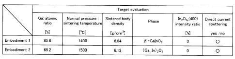
Table 1 shows target evaluation of embodiments 1 and 2 of a sintered body
according to the present invention.
\ ____________________________________ Target evaluation
Ga: atomic Normal pressure : Sintered body
In203p(400) Direct current
Phase
ratio sintering temperature density intensity
ratio sputtering
[%] [ C] [g/cm3] [ch] yes
/no
Embodiment 1 65.6 1400 6.04 -Galn03 0 0
Embodiment 2 65.2 1500 6.12 (Ga, In)203 0 0
Table 2 shows target evaluation of a first comparative example of the sintered
body.
Target evaluation
Ga: atomic Normal pressure : Sintered body
1n203p(400) Direct current
\\.\
Phase
ratio sintering temperature density intensity ratio
sputtering
\
[/h] [ C] [g/cm3] [ h] yes/no
Comparative
58.3 1400 6.28 $ -GaIn03, In203 7 0
example 1
Table 3 shows target evaluation of a third to eight embodiments of the
sintered
body according to the present invention.
\ Ga: atomic HP:sintering Sintered body
Phase
In203p(400) Direct current
ratio temperature density intensity ratio
sputtering
Pd [ C] [g/cm3] [%] yes/no
Embodiment 3 65.4 800 5.85 $ -GaIn03 0 0
_.
Embodiment 4 65.4 900 6.08 R -GaIn03 0 0
Embodiment 5 65.9 1000 6.12 B -Galn03, In203 5 0
Embodiment 6 79.8 900 5.72 13 -Ga203, /3 -GaInO, 0 0
Embodiment 7 89.9 900 5.51 $ -Ga203, /3 -GaIn03 0 0
Embodiment 8 99.1 900 5.02 $ -Ga203 0 x
Table 4 shows target evaluation of the second comparative example of the
sintered
body.
N Ph] temperature [ C]C] Target evaluation density
Ga:atomic ratio
HP:sintering
Sintered body
[g/cm3] Phase
In203p(400) Direct current
intensity ratio sputtering
[A] yes
/no
_
_
Comparative
example 2 65.3 1100 4.89 B -Galn03, 1n203 12 x
7
CA 02568966 2013-01-11
,
,
Table 5 shows thin film evaluation of embodiments 9 and 10 of the oxide film
according to the present invention.
Substrate
\
temperature
[ C][%] Ga:atomic ratio
Thin film evaluation
The shortest wavelength at light transmittance
50% except substrate
r
[nm] [nm] [nrn]
Embodiment 9 25 65.6 318
0.49
Embodiment 10 25 65.2 320
0.51
Table 6 shows thin film evaluation of a third comparative example of the oxide
film.
Substrate
\
temperature
[ C]{%] Ga:atomic ratio
Thin film evaluation
The shortest wavelength at light transmittance
50% except substrate
[nm] [nm] [nrn]
Comparative
25 58.7 332
0.55
example 3
Table 7 shows thin film evaluation of embodiments 11 to 14 of the oxide film
according to the present invention.
Substrate
\
temperature
[ C] [%]
ratio
DO [nm] Thin film evaluation
The shortest wavelength at light transmittance
50% except substrate
Ra
[nm]
Embodiment 11 25 65.5 318
0.48
Embodiment 12 25 79.7 296
0.52
Embodiment 13 25 90.2 284
0.51
Embodiment 14 25 99.5 269
0.51
Table 8 shows thin film evaluation of a fourth comparative example of the
oxide
film.
Thin film evaluation
Substrate
Ga:atomic ratio
\
The shortest wavelength at light transmittance
50% except substrate
[ C] [%]
[nm] Ra
temperature
[nm]
,
Comparative
25 59.7 340
0.62
example 4
7a
CA 02568966 2013-01-11
,
,
Table 9 shows thin film evaluation of embodiment 15 of the oxide film
according to
the present invention.
\ Thin film evaluation
\ Substrate The shortest wavelength at light
transmittance
Ga:atomic ratio Ra
temperature 50% except substrate
[ G] [%] [nrn] [nrn]
Embodiment 15 25 65.1 320
0.54
DETAILED DESCRIPTION OF THE PREFERRED EMBODIMENTS
The oxide sintered body, the oxide film, and the transparent base material
containing
it according to the present invention will be explained in detail hereafter.
However, the
present invention is not limited to the following embodiments.
The oxide sintered body according to the present invention, comprises an oxide
sintered body which mainly consists of gallium, indium, and oxygen, wherein a
content
of the gallium is more than 65 at.% and less than 100 at.% with respect to all
metallic
elements, and the density of the oxide sintered body is 5.0 g/cm3 or more.
Further, the oxide sintered body comprises gallium, a content of which is more
than
65 at.% and 90 at.% or less with respect to all metallic elements, and the
density of the
sintered body is 5.5g/cm3 or more, and when it is used as a sputtering target,
it is
possible to form a film by a direct current sputtering method.
Furthermore, the oxide sintered body according to the present invention is an
oxide
sintered body which mainly consists of gallium, indium, and oxygen. However,
if it is
7b
CA 02568966 2006-11-27
mainly constituted by the above-mentioned elements, other inevitable impurity
can be
included.
It is desired that the above-mentioned oxide sintered body is constituted by
one phase
or more phases selected from a gallium-oxide phase which has ti -Ga203 type
structure ( /3 -Ga203 phase), a gallium-indium-oxide phase having /3 -Ga203
type
structure (i3 -Galn03 phase), or (Ga, '0203 phases.
When the oxide sintered body has one phase or more phases selected from a
gallium-oxide phase which has 3 -Ga203 type structure ( /3 -Ga203 phase), a
gallium-indium-oxide phase which has /3 -Ga203 type structure ( /3 -GaIn03
phase), or
(Ga, In)203 phase phases, and it is constituted by an indium oxide phase
(In20:3 phase)
of bixbyite type structure, it is desirable that a ratio in which the indium
oxide phase
(In203 phase) of the bixbyite type structure is contained is 5% or less in
term of X-ray
diffraction peak intensity ratio defined by the following formula (1).
In203 phase (400) / 3 -Ga203 phase (-202) + /3 -GaIn03 phase (111)+(Ga,In)203
phase
(2 O 33 )1 x 100 [%] (1)
Here, information concerning the structure of each phase, has been clearly
shown by
JCPDS cards which are 41-1103 ( -Ga203 phase), 21-0334 ( /3 -GaIn03 phase),
14-0564((Ga,In)203 phase), and 06-0416 (1n203 phase).
Main peaks of 3 -GaIn03 phase and 1n203 phase in X-ray diffraction, are based
on
(111) reflection and (222) reflection, respectively, but, since 1n203 phase
(222) reflection
laps with /3 -GaIn03 phase (002) reflection, with respect to 1n203 phase it is
evaluated
by (400) reflection having the next highest intensity.
The oxide sintered body which does not have a metal indium phase can be
obtained by
sintering the oxide sintered body in an inert gas atmosphere, at 800t ¨1000`C
of
sintering temperature by a hot pressing method, and under the condition of
pressure
4.9MPa---29.4MPa,
When an oxide film is formed by the sputtering method, using these oxide
sintered
bodies as a sputtering target for example, it is possible to obtain an oxide
film such that
it has a composition range wherein it mainly consists of gallium, indium and
oxygen,
and a content of the gallium is more than 65 at.% and less than 100 at.% with
respect to
all metallic elements, and more preferably, more preferably has a composition
range
wherein a content of gallium is more than 65 at.% and 90 at.% or less with
respect to all
metallic elements, and a shortest wavelength is 320nm or less, where the light
transmittance of the film itself except a substrate is 50%.
8
CA 02568966 2006-11-27
Furthermore, in order to obtain the above-mentioned oxide film, it is desired
that a
film is formed using as a sputtering target, an oxide sintered body in which
generation
of an indium oxide phase (1n203 phase) of the bixbyite type structure, which
causes fall
of the light transmittance of an oxide film in the region of the wavelength of
400nm or
less, is suppressed.
The oxide sintered body according to the present invention mainly consists of
gallium,
indium and oxygen, and a content of the gallium is more than 65 at.% and less
than 100
at.% with respect to all metallic elements, and it is required that it is in a
composition
range excluding gallium-oxide.
Furthermore, it is required that the density of the oxide sintered body is 5.0
g/crill or
more.
Here, when a content of gallium is 65 at.% or less, to all metallic elements,
and an
oxide film is formed by using this oxide sintered body as a sputtering target
for example,
a shortest wavelength where the light transmittance of the film itself except
a substrate
is 50% exceeds 320nm.
Since sintering becomes remarkably difficult in a composition range of gallium-
oxide,
it becomes difficult to obtain a high-density oxide sintered body.
When sputtering is performed by using an oxide sintered body that has not yet
become high density, as a sputtering target, a problem occurs, namely,
abnormal electric
discharge of arc discharge etc. occur frequently, and consequently, the
shortest
wavelength where the light transmittance of the film itself except a substrate
becomes
50% is 320nm or less. Therefore, good quality oxide film cannot be obtained.
When the oxide sintered body having the density of the sintered body less than
5.0
g/cm3 is used as a sputtering target, generation of nodule and generating of
arc
discharge in long-time use occur, and film characteristics of the oxide film
obtained get
worse.
Furthermore, in the oxide sintered body according to the present invention, it
is more
desired that it contains gallium content of which is more than 65 at.% and 90
at.% or
less with respect to all metallic elements, and the density of the sintered
body is 5.5 g/
cm3 or more, and when it is used as a sputtering target, forming of a film can
be made
by a direct current sputtering method.
The reason is that since an oxide sintered body in this range has sufficient
conductivity and the density of the sintered body, abnormal electrical
discharge of arc
discharge etc. does not occur, and accordingly the direct current sputtering
can be
carried out successfully.
In a direct current sputtering method mentioned here, a sputtering method
(direct
9
CA 02568966 2006-11-27
current pulsing method) in which a negative voltage applied to a target is
ceased
periodically, and during the period, by applying a low positive voltage,
neutralization of
positive charging is carried out by electrons is also included.
The direct current pulsing method is desirable, since it has advantages such
that a
film can be formed while controlling arcing in a reactive sputtering using
reactant gas of
oxygen, and control of impedance consistency circuit like in the RF sputtering
method is
not required, and, film forming speed is quicker than that of the RF
sputtering method.
Further, it is desired that the oxide sintered body according to the present
invention is
constituted by one or more phases selected from a gallium-oxide phase which
has /3
-Ga203 type structure (13 -Ga203 phase), a gallium-indium-oxide phase having I
-Ga203
type structure (13 -GaIn03 phase), or (Ga, In)203 phases.
Furthermore, it is desired that the oxide sintered body according to the
present
invention is constituted by one or more phases selected from a gallium-oxide
phase
which has 13 -Ga203type structure (13 -Ga203 phase ), a gallium-indium-oxide
phase
having 13 -Ga203 type structure ( -GaIn03 phase), or (Ga,In)203 phases,
wherein it is
constituted by an indium oxide phase (1n203 phase) of bixbyite-type structure,
a ratio in
which the indium oxide phase (In203 phase) of the bixbyite-type structure is
contained
is 5% or less in term of X-ray diffraction peak intensity ratio defined by the
following
formula (1).
In203phase(400)/{ -Ga203}phase( 202)+ - [3 -
GaIn03 phase(111)+(Ga, In)203
phase(2 8#33" ) ) X 100 Ki (1)
If the X-ray diffraction peak intensity ratio of the formula is 5% or more,
since a
contribution to optical characteristics of the oxide film by the indium oxide
phase (In203
phase) having a bixbyite-type structure of a sputtering target is large, a
shortest
wavelength where the light transmittance of the film itself except a substrate
is 50%
exceeds 320nm.
Here, as for the indium oxide phase (1n203 phase) of bixbyite-type structure,
it may be
that in which oxygen deficit has been introduced, or a part of indium has been
replaced
by gallium. And, as for -Ga203 phase, it may be that in which oxygen deficit
has been
introduced, or it may be that in which a part of gallium has been replaced by
indium.
As for 13 -Galn03 phase and (Ga,In)203 phase, they may be those in which
oxygen
deficit is introduced, or in which the atomic ratio of gallium to indium is
somehow
shifted from their stoichiometry.
The oxide sintered body according to the present invention is desirable, since
an oxide
CA 02568966 2007-04-05
sintered body which does not contain a metal indium phase is obtained
according to the
oxide sintered body, wherein the oxide sintered body is sintered by the hot
pressing
method, and the sintering condition is such that in an inert gas atmosphere,
sintering
temperature is 800 C-1000 C and pressure is 4.9MPa-29.4MPa.
Sintering is not fully carried out at a sintering temperature less than 800 C
in an
inert gas, but when it exceeds 1000 C, metal indium is melted and it will ooze
out.
The range of a pressure of 4.9MPa-29.4MPa is desirable. When a pressure is
lower
than this range, the sintering is not carried out enough. Therefore, good
quality oxide
sintered body with high density cannot be obtained.
Even when the pressure is set at higher than this range, the density of the
sintered
body is not improved, and breakage of a mold used for the hot pressing occurs
easily.
Furthermore, an oxide film of the present invention is an oxide film obtained
using
the sputtering method, wherein the oxide sintered body is used as a sputtering
target,
and mainly consists of gallium, indium, and oxygen. The oxide film contains
gallium, a
content of which is more than 65 at.% and less than 100 at.% with respect to
all metallic
elements, and it has an outstanding characteristics such that a shortest
wavelength is
320nm or less, where the light transmittance of the film itself except a
substrate is 50%.
When a content of gallium is 65 at.% or less, to all metallic elements, as for
the oxide
film obtained, a shortest wavelength where the light transmittance of the film
itself
except a substrate is 50% exceeds 320nm.
Film of gallium oxide is not desirable, since as for the film of gallium
oxide, it is
difficult to obtain a high-density sintered body as mentioned above, and
accordingly, it
is difficult to obtain an oxide film having the shortest wavelength where the
light
transmittance of the film itself except a substrate is 50% becomes 320nm or
less.
It is desired that the oxide film according to the present invention is
obtained by the
direct current sputtering method which is an advantageous film forming method
industrially.
It is desired that the oxide film of the present invention is an amorphous
film.
This is because the amorphous film has a good etching nature as compared with
a
crystalline substance film, and, it is because a flatness nature of the
emulsion surface,
which is considered important in an electrode used especially for organic
electroluminescence (EL), is excellent.
Furthermore, in the oxide film of the present invention, it is desired that
the
arithmetic mean roughness (Ra) is 1.0 nm or less. Here, the arithmetic mean
roughness (Ra) is
based on the JIS B-0601 Standard (2001) of the Japanese Standards Association.
When the arithmetic mean roughness (Ra) exceeds 1.0 nm, it is not desirable in
a
11
CA 02568966 2006-11-27
particular use in which the flatness nature of an emulsion surface is
required, such as
organic EL.
The transparent base material of the present invention can be obtained by
forming
the oxide film of the present invention mentioned above on one surface side or
both
surface sides of a glass plate, a quartz plate, a resin plate or resin film
where one side or
both sides are covered by a gas barrier film, a transparent plate which were
selected
from a resin plate or a resin film where the gas barrier film is inserted in
the inside.
A thin film transistor (TFT) and a metal electrode for driving it can be
formed on the
transparent plate mentioned above, as long as the transparency of a substrate
is not
completely spoiled.
The above-mentioned resin plate or a resin film has the high permeability of
gas
compared with a glass plate, on the other hand, a luminescence layer of an
organic EL
device or inorganic EL element deteriorates by moisture or oxygen, when the
resin plate
or the resin film is used as a substrate of these display elements, it is
desirable to give a
gas barrier film which suppresses passage of gas.
As the gas barrier film, it is desirable to form one film or more films
between a
transparent plate and an oxide film.
It is desired that the gas barrier film is one film or more films selected
from a silicon
oxide film, an silicon oxide nitride (SiON) film, an aluminum acid magnesium
film, a tin
oxide type film, and a diamond-like carbon (DLC) film.
Further, not only an inorganic film but also an organic film may be included
in the gas
barrier film.
Here, tin oxide type film is defined that it has a composition which contained
one
element or more elements of additional elements selected from for example, Si,
Ce, Ge,
etc, in tin oxide.
By these additional elements, a tin oxide layer is made amorphous and a
precise film
is formed.
It is possible to use a composition such that the oxide film is formed on a
base
substrate wherein a gas barrier film that is one film or more films selected
from a
silicon oxide film, an silicon oxide nitride (SiON) film, an aluminum acid
magnesium
film, a tin oxide film, and a diamond-like carbon (DLC) film, and an organic
film or a
high polymer film are laminated repeatedly and alternately, on a surface of a
resin base
plate or a resin film.
The gas barrier film may be formed on one surface of the resin plate or the
resin film.
If it is formed on both surfaces, an interception function of gas passing
becomes further
better.
12
CA 02568966 2006-11-27
Further, by forming a gas barrier film on one surface side of the resin plate
or the
resin film, and further laminating the resin plate or the resin film on such
gas barrier
film, a composition in which the gas barrier film is inserted can be obtained.
Furthermore, it can be a composition in which laminating are made out
repeatedly.
It is desired that the resin plate or the resin film consists of polyethylene
terephthalate (PET), polyether sulfone (PES), polyarylate (PAR), polycarbonate
(PC), or
polyethylenenaphthalate (PEN), or lamination structure having a surface of
such
materials covered with acrylic organic substance. However, it is not limited
within the
scope mentioned above.
The thickness of the resin plate or the resin film is suitably selected
according to the
following concrete uses.
When using the transparent base material as an electrode of a device using
LEI), a
laser, an organic or inorganic EL, which emits blue and near-ultraviolet
light.
It is industrially useful, since it becomes possible to obtain high light
transmittance in a
visible light short wavelength region as well as a near-ultraviolet light
region of
wavelength.
Further, it is useful when it is used as an electrode for elements of a self-
luminescence type, such as an organic EL device etc., since an extraction
efficiency of
the light of the near-ultraviolet region can be raised.
Embodiment
Hereafter, the present invention will be explained more concretely by using
embodiments.
1) Production of an oxide sintered body
The sintered body has been produced by an atmospheric pressure sintering
method
described below.
Gallium oxide powder and indium oxide powder of purity 4N were grinded by a
ball
mill and adjusted to the average particle diameter of 3 micrometers or less,
respectively.
Then, they were blended so that the atomic ratio of gallium to all metallic
elements
might become to a desired ratio, and mixed with the ball mill with an organic
binder, a
dispersant, and a plasticizer for 48 hours, and consequently slurry was
produced.
Obtained slurry was dried out with a spray dryer, and granulation powder was
produced.
Then, obtained granulation powder was put into a rubber mold, and a forming
object
with 191mm 5, thickness of about 6mm was produced with a hydrostatic pressure
pressing machine.
In an oxygen gas flow, the forming object obtained by the same way was
sintered
13
CA 02568966 2007-04-05
under an ordinary pressure at a predetermined temperature (it is shown in an
embodiment) for 20 hours.
In addition to the atmospheric pressure sintering method, the oxide sintered
body
was produced also by the hot pressing method.
Then, the gallium oxide powder and the indium oxide powder were blended so
that
the atomic ratio of gallium to all metallic elements might become to a desired
ratio, and
then, they were agitated by a three-dimensional mixer and precursor powder was
produced.
By supplying mixed powders obtained into a container made of carbon, sintering
was
carried out using the hot pressing method under each of conditions.
In order to prevent degradation by oxidization of the container made of
carbon, it was
carried out in Ar gas atmosphere.
The pressure was fixed to 24.5MPa, sintering temperature was made at a
predetermined temperature (it is shown in an embodiment), and sintering time
was set
constant in 3 hours.
Then, circumference processing and surface grinding processing were given to
the
obtained sintered body, and it was made about 15.24cm (6 inches) in diameter,
and
formed about 5mm in thickness.
After the processing, bonding of the sintered body was carried out to a copper
plate for
cooling, and a sputtering target was obtained.
2) Production of a thin film
TM
TOKU SPF-530H (manufactured by ANELVA) was used for sputtering equipment.
A synthetic quartz plate was used as a substrate, and it was arranged so that
it may
become parallel to a target surface.
Distance between the substrate and the target was set to 60 mm.
Sputtering gas was mixed gas which consisted of argon and oxygen, and total
gas
pressure was set to 0.5 Pa while oxygen ratio was set to 1.0% to 2.0%.
Electrical power used was set to 200W.
Film forming by direct-current magnetron sputtering was carried out under
conditions mentioned above.
According to a target to be used, sputtering-time was adjusted and a thin film
with
200nm in thickness was formed.
In case that the direct current sputtering was unable to be used, the film was
formed
by sputtering of direct current pulsing method.
Other sputtering conditions were set to be equivalent to those of the direct
current
sputtering.
14
CA 02568966 2007-04-05
3) An oxide sintered body and thin film evaluation
As for the oxide sintered body and the thin film which were obtained, the
atomic ratio
of gallium to all metallic elements, was computed from weights of indium and
gallium
which were obtained by ICP emission spectral analysis method (SPS4000 made by
Seiko Instruments Inc. was used).
The density of the oxide sintered body was measured using pure water by
Archimedes
method (Automatic Densimeter-H made by TOY SEIKI SEISAKU-SHO, Ltd was
used).
The film thickness of the oxide film was measured with a surface profiler
(Alpha-Step
IQ made by KLA-Tencor co., Ltd.).
The specific resistance of the oxide sintered body and the oxide film was
computed
from =the surface resistance measured by the four probe method (LORESTA-II!
MCP-T250 made by Mitsubishi Chemical was used).
The light transmittance (Ts+F (%)) of the oxide film including the substrate
was
measured with a spectrophotometer (U-4000 made by the Hitachi, Ltd.).
Under the same conditions, the light transmittance (Ts (%)) of a substrate
only was
also measured, and (Ts+F/Ts) x100 was computed as light transmittance (TF (%))
of the
film itself excluding the substrate.
The X-ray diffractions of the oxide sintered body and the oxide film were
measured
with X-ray diffraction equipment (CuK a -rays made by the Rigaku Industrial
Co. was
used).
As to the oxide sintered body, a peak intensity was obtained by 1n203 phase
(400), 8
-Gaz03 phase (-202), 13 -GaIn03 phase (111) and (Ga, In)203 phase (2 O# 3 3
). Then,
a peak intensity ratio of 1n203 phase (400) expressed by the following formula
(1) was
calculated.
In203 phase (400) /1 -Ga203 phase(¨ 202)+13 -GaIn03 phase (111)+(Ga,In)203
phase(2
# 33 )) x100 P/ol (1)
The arithmetic mean height (Ra) was measured by an atomic force microscope
(Nanoscope III AFM, made by Digital Instruments Corp. was used).
(Embodiments 1 and 2)
Indium oxide powder and gallium oxide powder were blended so that the atomic
ratio
of gallium to all metallic elements might become 65.5 at.%, and the
atmospheric
pressure sintering was carried out under two conditions where sintering
temperatures
were at 1400 C and 1500 C, and consequently, the sputtering target was
produced.
CA 02568966 2013-01-11
Next, the direct current sputtering was tried at room temperature using these
two
kinds of sputtering targets.
An evaluation result of the targets was shown in Table 1.
As shown in Table 1, when the sintering temperature of the embodiment 1 was
1400 C,
the atomic ratio of gallium to the all metallic elements of the obtained oxide
sintered
body was 65.6 at.%.
Here, the density of the oxide sintered body was 6.04 g/cm3, and the phase
which
constitutes the sintered body was t3 -GaIn03 phase.
Therefore, the peak intensity ratio of In20:3 phase (400) expressed with the
formula
(1) mentioned above was 0%.
When the sintering temperature of the embodiment 2 was 1500 C, the atomic
ratio of
gallium to all metallic elements was 65.2 at.%, the density of the sintered
body was 6.02
g/cm3, the formed phase was only (Ga,In)203 phase, and the peak intensity
ratio of In203
phase (400) expressed with the formula (1) mentioned above was 0%.
When the direct current sputtering was carried out at room temperature using
these
two kinds of sputtering targets, any abnormalities, such as arc discharge,
were not seen,
and it was confirmed that the sputtering was successful.
(Comparative example 1)
Except having set the atomic ratio of gallium to all metallic elements was
58.5 at.%, a
sputtering target was produced as same to the embodiment 1, and direct current
sputtering was tried.
The evaluation result of the target was shown in Table 2.
As shown in Table 2, in the comparative example 1, the atomic ratio of gallium
to all
metallic elements of the sintered body was 58.3 at.%, and the density of the
sintered
body was 6.28 g/cm3.
The sintered body is constituted by (3 -GaIn03 phase and In203 phase, and the
peak
intensity ratio of In203 phase (400) expressed with the formula (1) mentioned
above was
7%.
In the direct current sputtering at room temperature using the sputtering
target,
no abnormality such as arc discharge was seen, and it was confirmed that the
sputtering was carried out successfully.
(Embodiments 3 to 8)
Indium oxide powder and gallium oxide powder were blended so that the atomic
ratio
of gallium to all metallic elements might vary 65.5 ¨99 at.%, and sintering
was carried
out by the hot pressing method under three conditions of sintering temperature
at
800 C ¨ 1000 C,and consequently, the sputtering target was produced.
16
CA 02568966 2013-01-11
Then, the direct current sputtering was tried at room temperature using these
three kinds of sputtering targets.
An evaluation result of the targets was shown in Table 3.
As shown in Table 3, in the cases of Embodiments 3-8, the atomic ratio of
gallium to all
metallic elements was 65.4 to 99.1 at.%, and the density of the sintered body
was 5.02 to
6.12 g/cm3, and consequently, good sintered body was obtained.
Next, it was confirmed that these sintered bodies are constituted by the f3 -
GaIn03
phase, /3 -Ga203, or the these two phases.
The peak intensity ratio of In20.3 phase (400) expressed with the above-
mentioned
formula (1) was 0% also in each of cases.
However, only in the embodiment 5, generation of In203 phase was seen, and the
peak
intensity ratio of In203 phase (400) expressed with the formula (1) mentioned
above was
5%.
When the direct current sputtering was carried out at room temperature using
these
oxide sintered bodies as sputtering targets, in embodiments 3-7, namely, in a
range
where the atomic ratio of gallium to all metallic elements was 65.4-89.9 at.%,
any
abnormalities, such as arc discharge, were not seen, and it was confirmed that
the
sputtering was carried out successfully. However, in case that the atomic
ratio of
gallium to all metallic elements of the embodiment 8 was 99.1 at.%, the direct
current
sputtering method was not possible.
(Comparative example 2)
Except that the hot pressing method was carried out at a sintering temperature
of
1100 C, the sputtering target was produced as same as in embodiments 3 and 4,
and the
direct current sputtering method was tried.
An evaluation result of the target was shown in Table 4.
As shown in Table 4, the atomic ratio of gallium to all metallic elements was
65.3 at.%
in the comparative example 2, but the density of the sintered body was low as
4.89 g/cm
and good sintered body was not able to be obtained.
A trace showing that during sintering Indium was melted and oozed was seen.
The sintered body is constituted by /3 -GaIn03 phase, In phase, and 1n203
phase, and
the peak intensity ratio of In203 phase (400) expressed with the formula (1)
mentioned
above was high, that is 12%.
This is presumed to be due to the melting and oozing of indium.
In the direct current sputtering at room temperature using the sputtering
target,
Arc discharge occurs frequently, and consequently good sputtering state was
not
acquired.
17
CA 02568966 2013-01-11
(Embodiments 9 and 10)
By using the sputtering target produced in embodiments 1 and 2, the direct
current
sputtering was carried out at the room temperature, and thin films were
formed.
Evaluation results of the obtained films are shown in Table 5.
The atomic ratio of gallium to the all the metallic elements of the films
obtained by
the ICP emission spectral analysis method, were 65.6 at.% and 65.2 at.%, where
the
composition of the sputtering targets in embodiments 1 and 2 were reproduced.
The shortest wavelength where the light transmittance of the film itself
excluding the
substrate becomes 50% was 320nm or less in each case.
As for the arithmetic mean height (Ra), it was confirmed that all were around
0.5nm,
and 1.0nm or less.
As the result of the X-ray diffraction measurement of the obtained films, it
was also
confirmed that it was an amorphous film in each case.
It was shown that these films had electric conductivity and, the specific
resistance of
embodiments 9 and 10 were 7.1 x 10⁻¹ ,(2 = cm and 6.3X 10⁻¹ O = cm,
respectively.
(Comparative example 3)
By using the sputtering target produced in the comparative example 1, the
direct
current sputtering was carried out at room temperature, and a thin film was
formed.
An evaluation result of the obtained film is shown in Table 6.
The atomic ratio of gallium to the all metallic elements of the obtained film
by the ICP
emission spectral analysis method, was 58.7 at.%, where the composition of the
sputtering target in the comparative example 1 was reproduced.
However, the shortest wavelength where the light transmittance of the film
itself
excluding the substrate becomes 50% was 332nm. It did not become 320nm or
less.
However, as for the arithmetic mean height (Ra), it was confirmed that it was
around
0.5nm, and 1.0nm or less.
As a result of the X-ray diffraction measurement of the obtained film, it was
confirmed that it was an amorphous film.
It was shown that this film had conductivity and its specific resistance was
1.1 x 10⁻¹
O cm.
(Embodiments 11 to 14)
In embodiments 4, and 6 to 8, thc puttering targetc were produced by the hot
pressing method on condition of a sintering temperature of 900 C. The direct
current
sputtering was carried out at the room temperature, and thin films were formed
using
them.
Since by the sputtering target of embodiment 8, the direct current sputtering
was
18
CA 02568966 2013-01-11
unable to be carried out, the thin film was formed by sputtering by the direct
current
pulsing method.
Evaluation results of the obtained thin films are shown in Table 7.
The atomic ratio of gallium to the all metallic elements of the thin films
obtained by
the ICP emission spectral analysis method, were 65.5 at.% to 99.5 at.%, where
the
composition of the sputtering targets in embodiments 4 to 7 were mostly
reproduced.
The shortest wavelength where the light transmittance of the film itself
excluding the
substrate becomes 50% was 320nm or less in each case.
Further, it was confirmed that the arithmetic mean height (Ra) is all around
0.5nm,
and it is 1.0nm or less in each case.
It was confirmed, as a result of the X-ray diffraction measurement of the
obtained
film, that it was an amorphous film in each case.
It was shown that the film of embodiment 10 had electric conductivity and its
specific
resistance was 5.8x 10⁻¹ t2 -cm.
However, it was not shown that other films had electric conductivity.
(Comparative example 4)
By using the sputtering target produced in the comparative example 2, an oxide
film
was formed by sputtering.
However, since by the sputtering target of this comparative example 2, direct
current
sputtering could not be carried out, the thin film was formed by sputtering by
a direct
current pulsing method at room temperature.
An evaluation result of the obtained film is shown in Table 8.
As to the atomic ratio of gallium to all metallic elements of the thin film,
which was
obtained by the ICP emission spectral analysis method, it was 59.7 at.%, where
gallium
was less than composition of the sputtering target of the comparative example
2.
And, the shortest wavelength where the light transmittance of the film itself
excluding the substrate becomes 50% was 340nm, which did not become 320nm or
less.
However, as for the arithmetic mean height (Ra), it was confirmed that it was
0.62nm,
and 1.0nm or less.
As a result of the X-ray diffraction measurement of the film obtained, it was
confirmed that it was an amorphous film.
It was shown that this film had electrical conductivity and its specific
resistance was
2.2 X 10⁻¹ ûcm.
(Embodiment 15)
By using the sputtering target produced by the hot pressing method under
condition
of sintering temperature 1000 C in embodiment 5, the direct current sputtering
was
19
CA 02568966 2013-01-11
carried out at room temperature, and a thin film was formed.
An evaluation result of the thin film obtained is shown in Table 9.
The atomic ratio of gallium to the all metallic elements of the thin film
obtained by
the ICP emission spectral analysis method, were 65.1 at.%, where the
composition of the
sputtering target in embodiment 5 was mostly reproduced.
The sputtering target of embodiment 5 contained indium oxide phase (1n203
phase) of
bixbyite-type structure, which was 5% in term of the peak intensity ratio of
In203 phase
(400) expressed with the formula (1) mentioned above. Nevertheless, the
shortest
wavelength where the light transmittance of the film itself excluding the
substrate
becomes 50% was 320nm or less.
As for the arithmetic mean height (Ra), it was around 0.5nm. Thus, it was
confirmed
that it was 1.0nm or less.
As a result of the X-ray diffraction measurement of the film, it was confirmed
that it
was an amorphous film.
It was shown that the obtained film had electric conductivity and its specific
resistance was 5.1 x 10-10 = cm.
(Embodiment 16)
Except that PET film (made by Toyobo Co., Ltd.) having 100m in thickness was
used
for a substrate, a thin film was formed on one of surfaces of the PET film
under the
same conditions as embodiment 9.
It was confirmed, by X-ray diffraction like in embodiment 9, that an obtained
transparent conductive oxide film was an amorphous film.
As shown in embodiment 9, the shortest wavelength where the light
transmittance of
the film itself excluding substrate becomes 50% was 320nm or less.
Nevertheless, the
shortest wavelength where the light transmittance becomes 50% when the PET
film
was included was 324nm, which was equivalent to 322nm in case of the PET film
itself.
It was confirmed that the arithmetic mean height (Ra) was 1.0nm or less.
(Embodiment 17)
Except that a substrate having a barrier film in which a silicon-oxide-nitride
film
was formed on both surfaces of the PES film (made by Sumitomo Bakelite Co.,
Ltd.) of
200m in thickness was used as a substrate, a film was formed on both of
surfaces of the
film under the same conditions as embodiment 12.
It was confirmed, by X-ray diffraction like in the embodiment 12, that the
obtained
transparent electric conduction film was an amorphous film.
As shown in embodiment 12, the shortest wavelength where the light
transmittance
of the film itself except the substrate becomes 50% was 320nm or less.
Nevertheless,
, CA 02568966 2013-01-11
the shortest wavelength where the light transmittance becomes 50% when the PES
film
was included was 350nm, which was equivalent to 350nm in case of the PES film
itself.
It was confirmed that the arithmetic mean height (Ra) was 1.0nm or less.
Evaluation
From results in embodiments 1 to 8, it has been clear that no abnormal
electric
discharge such as arc discharge etc., occurs, and accordingly a good
sputtering can be
achieved, when a sputtering is carried out using as a sputtering target, the
oxide
sintered body of the present invention characterized in that an oxide sintered
body
which mainly consists of gallium, indium, and oxygen, wherein a content of
which is
more than 65 at.% and less than 100 at.% with respect to all metallic
elements, and the
density of the sintered body is 5.0 g/cm3 or more.
In particular, from results of embodiments 1 to 7, it has been clear that no
abnormal
electric discharge such as arc discharge etc., occurs, and accordingly a good
sputtering
can be achieved, when the sputtering is carried out using as a sputtering
target, an
oxide sintered body of the present invention characterized in that an oxide
sintered
body wherein a content of gallium of the present invention is more than 65
at.% and less
than 90 at.% with respect to all metallic elements, and the density of the
sintered body
is 5.5 g/cm3 or more.
From the result of embodiments 3 to 8, it has been clear that no abnormal
electrical
discharge such as arc discharge etc., occurs, and accordingly the direct
current
sputtering can be carried out successfully, when an oxide sintered body of the
present
invention is used as a sputtering target, that is characterized in that an
oxide sintered
body which is sintered by the hot pressing method in an inert gas atmosphere
under
conditions in which sintering temperature is 800 C-1000C and sintering
pressure is
4.9MPa-29.4MPa, and it does not contain metal indium phase.
Next, from the result of embodiments 9 to 15, it has been shown that the oxide
film of
the present invention namely, an oxide film obtained by using a sputtering
method,
wherein the oxide sintered body according to embodiments 9 to15 is used as a
sputtering target, is an oxide film which consists of gallium, indium, and
oxygen,
wherein the oxide film has gallium, a content of which is more than 65 at.%
and less
than 100 at.% with respect to all metallic elements, and a shortest wavelength
where
the light transmittance of the film itself excluding a substrate becomes 50%,
is 320nm
or less, and it is an amorphous film and its arithmetic mean height (Ra) is
1.0nm or less.
In particular, from embodiment 15, it has been shown that the shortest
wavelength
where the light transmittance of the film itself excluding a substrate becomes
50% is
320nm or less, if an oxide film is obtained by using as a sputtering target,
the oxide
21
CA 02568966 2006-11-27
sintered body according to the present invention, that is, an oxide sintered
body
characterized in that it has one phase or more phases selected from a gallium-
oxide
phase which has -Ga203 type structure (13 -Ga203 phase), an gallium indium
oxide
phase having /3 -Ga203 type structure ( -GaIn03 phase), or (Ga, In)203 phases,
wherein it is constituted by an indium oxide phase (In203 phase) of bixbyite-
type
structure, and a ratio of the contained indium oxide phase (1n203 phase) in
the
bixbyite-type structure is 5% or less in term of the X-ray diffraction peak
intensity ratio
defined by the following formula (1),
1n203 phase (400) / -Ga203 phase (¨ 202) + -Galn03 phase(111) +(Ga,In)203
phase (2 (i 33 )) x 100 [%] (1)
Contrary to this, it has been shown that in case of the oxide film in the
comparative
example 3, that is, an oxide film obtained by the sputtering method, using as
a
sputtering target, an oxide sintered body which does not satisfy the
composition range
of the comparative example 1, the shortest wavelength where the light
transmittance of
the film itself excluding a substrate becomes 50% exceeds 320nm.
It has been also shown that the shortest wavelength where the light
transmittance of
the film itself excluding a substrate becomes 50% exceeds 320nm with respect
to an
oxide film obtained by the sputtering method, by using as a sputtering target,
an oxide
sintered body in which the hot press conditions of the comparative example 1
are not
satisfied, and the ratio of the contained indium oxide phase (1n203 phase)
having the
bixbyite-type structure exceeds 5%.
From embodiments 16 and 17, it has been confirmed that the transparent base
material according to the present invention, that is, the transparent base
material
characterized in that the oxide film of the present invention is formed on one
surface or
both surfaces of a transparent plate of a resin film wherein one surface or
both surfaces
are covered with a gas barrier film can be obtained.
22