Note: Descriptions are shown in the official language in which they were submitted.
CA 02569018 2010-05-28
PU040180
SYSTEM AND METHOD FOR ROUTING ASYNCHRONOUS SIGNALS
FIELD OF THE INVENTION
[0002] This invention relates to routers and more specifically to broadcast
routers
that route asynchronous signals.
BACKGROUND OF THE INVENTION
[0003] A router comprises a device that routes one or more signals appearing
at
the router input(s) to one or more outputs. Routers used in the broadcast
industry
typically employ at least a first router portion with a plurality of router
modules (also
referred to as matrix cards) coupled to at least one expansion module. The
expansion
module couples the first router chassis to one or more second router portion
to allow
further routing of signals. Many broadcast routers, and especially those that
are linearly
expandable, route asynchronous signals. Asynchronous signal routing by such
linearly
expandable routers requires an accurate clock signal throughout the entire
route to
preserve the integrity of routed data. For an asynchronous signal, a
difference in clock
frequency from one location to another can cause corruption of the signal and
loss of the
data represented by that signal. Even a difference in clock frequencies as
small as 1 part
per million (PPM) can have an undesirable effect on data. Typical examples of
data
corruption include repeated or dropped signal samples.
[0004] As linearly expandable routers increase in complexity, the problem of
supplying an accurate and synchronized clock signal to various elements
becomes more
difficult. For purposes of discussion, a clock signal constitutes a signal
that oscillates between
CA 02569018 2012-12-21
PU040180
- 2 -
a high and a low state at defined intervals. Typical clock signals oscillate
with a 50% duty
cycle. However, clocks having other duty cycles are also commonly employed.
Circuits
using clock signals for synchronization become active upon one of the rising
or falling
edge of the clock signal.
10005] A so-called, "clock multiplexer" refers to a circuit, as typically
exists
within a linearly expandable router, for selecting at least one clock signal
from a plurality
of available clock signals. The selected clock signal(s) serve to trigger
other elements.
When selecting among available clock signals, the output signal selected by
the clock
multiplexer should not include any undefined pulses. Undefined pulses occur,
for example,
when a selected clock signal undergoes a disruption. Such a disruption can
include a
missing clock signal as well as a clock signal that fails to switch states as
expected. Some
times, an input clock signal will remain "stuck" indefinitely at one logic
state or the other.
Such disruptions frequently produce undefined pulses including runt pulses,
short pulses,
pulses of indefinite duration, glitches, spikes and the like.
[0006] Prior art attempts to avoid undefined pulses at the output of a clock
multiplexer include so-called "safe" clock multiplexers. A typical safe clock
multiplexer
switches from a presently selected input to a next selected input in an
orderly manner.
Thus, a safe multiplexer does not switch until the selected input clock signal
transitions to a
known state and the subsequently selected clock signal transitions to the same
state as the
previously selected clock signal.
[0007] However, prior art safe clock multiplexers have drawbacks. For example,
when a presently selected clock signal fails to transition to a known state, a
safe clock
multiplexer will often lack the ability to switch to another clock signal.
Prior art safe clock
multiplexers have not tolerated these and other types of clock disruptions.
[0008] Thus, a need exists for a technique for providing a selected one of a
set of
clock signals, such as within a linearly expandable router, that overcomes the
aforementioned disadvantages
SUMMARY OF THE INVENTION
[0009] Briefly in accordance with a preferred embodiment of the present
principles,
there is provided a method for selecting a clock signal from among at least
first and second clock
CA 02569018 2006-11-24
WO 2006/009605 PCT/US2005/019115
-3-
signals. The method commences by detecting a failure of a first clock signal
to change state
and by detecting a failure of a second clock signal to change state. A
selection occurs from
among the first and second clock signals and an oscillator signal, based in
part on whether at
least one of the first and second clock signals has toggled
BRIEF DESCRIPTION Of THE DRAWINGS
[0010] FIGURE 1 illustrates a block schematic diagram of a router according to
an
illustrative embodiment of the present principles:
[0011] FIGURE 2 illustrates a first alternate arrangement of input and output
modules
for the router of FIG. 1
[0012] FIGURE 3 illustrates a second alternate arrangement of input and output
modules for the router of FIG. 1;
[0013] FIGURE 4 illustrates a third alternate arrangement of input and output
modules
for the router of FIG. 1
[0014] FIGURE 5 illustrates a first network of clock selector circuits for use
in the
router of FIG. 1;
[0015] FIGURE 6 depicts a second network of clock selector circuits for use in
the
router of FIG. 1
[0016] FIGURE 7 depicts a block schematic diagram of an illustrative
embodiment of
a clock selector circuit within the networks of FIGS. 5 and 6; and
[0017] FIGURE 8 depicts a safe clock multiplexer system of for use in the
selector
circuit of FIG. 4.
DETAILED DESCRIPTION
[0016] FIGURE 1 depicts a block schematic of a broadcast router 100 in
accordance
with a preferred embodiment of the present principles. In a preferred
embodiment, the router
100 comprises at least one, and preferably a plurality input modules 4021,
4022-402, where x
is an integer greater than zero, and at least one, and preferably, a plurality
of output modules
4041 ...404y, where y is an integer. Each input module, such as input module
4021, comprises
at least one, and preferably a plurality of input cards 4061, 4062...406z
where z is an integer
CA 02569018 2006-11-24
WO 2006/009605 PCT/1JS2005/019115
-4-
greater than zero. Each input card has at least one, and preferably, a
plurality of inputs for
receiving signals for multiplexing into an output signal. Different input
cards typically have
different signal receiving capabilities to afford the ability to receive
signals from a variety of
sources. An expansion card 408 within each input module, such as module 402i,
multiplexes
the output signals from the input cards 406[-406, into an output signal.
[0017] Each second module, such as second module 4041, has a matrix 410 card
which
de-multiplexes the input signals from one or more of the input modules for
delivery to at least
one, and preferably a plurality of output cards 412g, 4122...412p, where p is
an integer greater
than zero. Each output card delivers one or more output signals to one or more
external
devices (not shown). A control card 414 controls the matrix card 410 in
response to an
external control signal C to cause the matrix card to route its output signal
among various of
the output cards 4121-412p. In this way, the matrix card 410 can effectuate
routing based on
the external control signal C. =
[0018] The router 100 of FIG. 1 has each of its input modules 4021,
4022...402x
coupled to each of the output modules 404, 4022-404 Other arrangements are
possible.
FIGURE 2 illustrates a first alternate arrangement of input and output cards
for the router 100
of FIG. 1 wherein the input and output modules are arranged to provide the
same number of
inputs and outputs. FIGURE 3 illustrates a second alternate arrangement of
input and output
modules for the router 100 of FIG. 1 in which there are more inputs than
outputs. FIGURE 4
illustrates a third alternate arrangement of input and output modules for the
router 100 of FIG.
1 in which there are more outputs than inputs.
[0019] The input modules 4021-402x and the output modules 4041-404y of FIG. 1
typically each include at least one of clock modules 5001-500õ where n > x +
y, with each
clock module having a structure as described in greater detail with respect to
FIG. 5. In
practice, separate clock modules can exist in within one or more the elements
within each
input and output module of FIG. 1. Moreover, one or more clock module 5001-
500õ could
exist as separate modular elements in the router 100, much like one of the
input or output
modules.
[0020] Referring to FIG. 5, the clock modules 5001-500õ can interconnect with
each
other in a daisy chain fashion to yield a network 600 of clock modules. In the
embodiment of
FIG. 5, the clock module 5001 supplies its clock signal to the clock module
5002 as well as
each of clock modules 5003, 5004] and 50043, where i < n, whereas the clock
module 5002
CA 02569018 2006-11-24
WO 2006/009605 PCT/US2005/019115
-5-
supplies its clock signal to each of modules 500i, 50014 and 500+4. Each of
the clock
modules 5001, 5002-500õ also receives the clock signal from a preceding one of
clock
modules 5002...500i...500õ.i, respectively.
100211 FIGURE 6 depicts an alternate arrangement of clock modules wherein the
modules are arranged in first and second networks 6001 and 6002, with each of
the networks
6001 and 6002 configured similarly to the clock module network 600 of FIG. 2.
As seen in
FIG. 6, one or more of the individual clock modules 5001-500õ of network 6001
provide clock
signals to one or more of the clock modules 5001-500õ of network 6002. ,
[0022] FIGURE 7 depicts a block schematic diagram of an exemplary clock module
5001. The clock module 500; of FIG. 4 includes first and second clock inputs
that receive first
and second clock signals Clock_l and Clock_2, respectively. Each of the
external clock
signals Clock_l and Clock_2 can comprise clock signals from a separate
upstream clock
selector circuit in the network of FIG 2 or a clock signal from a reference
clock circuit formed
by an oscillator 508.
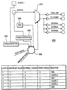
[0023] The clock selector circuit 500, includes a pair of toggle detectors 502
and 504
which each receive a separate one of the Clock_l and Clock_2 signals. Each
toggle detector
provides an output signal indicative of whether its respective input clock
signal has toggled,
i.e., a changed from one state to another. A logic block 506 receives the
output signals of the
toggle detectors 502 and 504, along with the output of an oscillator circuit
508 that generates a
clock signal useful for meeting the timing requirements of various circuit
elements. The logic
block 506 also receives two external status signals; (1) A_not B and (2)
Master_not Slave.
The state of the status signal A_not B indicates whether or not the clock
circuit 500; will
provide the primary clock signal. The state of the Master_not Slave signal
determines the
clock circuit 500, operates as its own master, or as a slave to another clock
signal.
[0024] The logic block 506 generates an output control for controlling a safe
clock
multiplexer system 510 to select among the clock signals Clock_1, Clock_2 and
the output
signal of the oscillator 508, to provide a single clock signal to downstream
elements (not
shown). The output control signal of the logic block 506 has a prescribed
relationship to the
logic circuit input signals as shown in Table 1, with the "x" entries
constituting "don't care"
values. (In other words, the value of the particular input signal has no
effect on the output of
the logic block 506.)
CA 02569018 2006-11-24
WO 2006/009605 PCT/US2005/019115
-6-
TABLE I
A_not B Master_Not Toggle Toggle Safe clock
Slave Detector 504 Detector 502 multiplexer
system 510
Output
1 x x Oscillator 508
0 1 1 Clock_2
0 1 x 0 Oscillator 508
0 1 x Clock_I
0 0 1 Clock_2
0 0 0 Oscillator. 508
[0025] As seen from Table 1, for so long as the Master_ Not Slave signal
remains at a
logic "1" level, the clock circuit 500i only selects between Clock_2 and
Oscillator 508. Under
such conditions, the toggling of the Clock_l signal, and hence the output
signal of the toggle
detector 504 has no effect. Conversely, when the clock circuit 500i serves as
a slave (i.e., the
Master_ Not Slave signal remains at a logic "0" level), the output states of
the toggle detector
504, and the output state of the toggle detector 502, determine which of the
Clock_1, Clock_2,
and oscillator 508 signals appear at the output of the safe clock multiplexer
system 510. The
clock signal selected by the safe clock multiplexer system 510 provides a
timing signal for
local use as well as for input to elements within the router 100 of FIG. I.
[0026] In a preferred embodiment, the safe clock multiplexer system 510 of
FIG. 4 has
the structure shown in FIG. 5 to afford the clock module 500; of FIG. 3 the
ability to tolerate
an input clock pulse that has become stuck. Within the safe clock multiplexer
system 510 of
FIG. 5, first and second toggle detectors 7011 and 7012 receive the Clock_l
and Clock_2
signals, respectively, as do each of a pair of multiplexers 7021 and 7022,
respectively. Each of
the multiplexers 7021 and 7022 receives a signal and a logic "0" level at its
second input.
[0027] The toggle detectors 7011 and 7012 control the multiplexers 7021 and
7021 in
accordance with the state of Clocki and Clock_2 signals, respectively, as
measured against
the output signal of the oscillator 508. In other words, each of the toggle
detectors 7011 and
7012 determines whether a respective one of the Clock.) and Clock_2 signals
has changed
state (i.e., toggled) relative to the output signal of the oscillator 508. If
a respective one of the
CA 02569018 2006-11-24
WO 2006/009605
PCT/US2005/019115
-7-
toggle detectors 7011 and 7012 determines that a corresponding one of the
Clock_l and
Clock_2 signals has toggled relative to the oscillator 508 output signal, then
that toggle
detector gates a corresponding one of the multiplexers 7021 and 7022. When
gated, each of
the multiplexers 7021 and 7022 passes and associated one of the Clock_l and
Clock_2 signals.
Should a respective one of the clock signals Clock_l and Clock_2 not toggle
relative to the
oscillator 508 output signal, then the corresponding one of the multiplexers
7021 and 7022 will
output a logic zero level signal.
[0028] A multiplexer 704 receives at its first and second inputs the output
signals of
the multiplexers 7021 and 7022, respectively. In accordance with a signal from
the logic block
506 of FIG. 4, the multiplexer passes the output signal of one of the
multiplexers 7021 and
7022 to a first input of a multiplexer 7061 and to the input of a toggle
detector 7081. The
multiplexer 7061 has its second input supplied with a signal at a logic zero
level.
[0029] The toggle detector 7081 controls the multiplexer 7061 in accordance
with the
relationship between the output signal of the multiplexer 704 and the output
signal of the
oscillator 508. In other words, the toggle detector 7081 determines whether
the output signal
of the multiplexer 704 has changed state relative to the output signal of the
oscillator 508. If
the output signal of the multiplexer 704 toggles relative to the oscillator
508 output signal,
then the toggle detector 7081 causes the multiplexers 7061 to pass the output
signal of the
multiplexer 704. Otherwise, should the output signal of the multiplexer 704
not toggle
relative to the output signal of the oscillator 508, the multiplexer 7061 will
output a logic zero
level signal.
[0030] A multiplexer 7062 receives at its first and second inputs the output
signal of
the oscillator 508 and a logic zero level signal, respectively. A toggle
detector 7082 controls
the multiplexer 7062 in accordance with the oscillator 508 output signal. In
other words, the
toggle detector 7082 determines whether the output signal of the oscillator
508 periodically
changes state. If the oscillator 508 output signal does toggle, then the
toggle detector 7082
gates the multiplexer 7062 to pass the output signal of the oscillator 508.
Otherwise, should
the output signal of the oscillator 508 not toggle, then the multiplexer 7062
will output a logic
zero level signal.
[0031] A multiplexer 710 receives at its first and second inputs the output
signals of
the multiplexers 7061 and 7062, respectively. Like the multiplexer 704, the
multiplexer 710
operates under the control of the logic block 506 of FIG. 4. Thus, depending
on output signal
CA 02569018 2006-11-24
WO 2006/009605 PCT/US2005/019115
-8-
of the logic block 506, the multiplexer 710 will either output a selected one
of the Clock_l
and Clock...2 signals (assuming at least one has toggled relative to the
oscillator 508 output
signal) or the output signal of the oscillator 508 (assuming it has toggled.)
[0032] An important distinction exists between the multiplexers 702, and 7022
and the
multiplexers 704 and 710. The multiplexers 704 and 710 serve as clock
multiplexers as
described earlier. Advantageously, described, the safe clock multiplexer
system 510 of FIG. 5
precludes the possibility of a missing clock pulse. By controlling the passage
of the Clock_l
and Clock_2 signals relative to the oscillator 508 output signal and by
controlling the passage
of the oscillator 508 output only if it has toggled, the safe clock
multiplexer system 510 avoids
a situation in which any or all of the clocks become stuck in a no-clock
state:
[0033] The foregoing describes a clock selector circuit 500i, including a safe
multiplexer system 510, for distributing clock pulses so as to provide for
redundancy while
assuring clock synchronism.