Note: Descriptions are shown in the official language in which they were submitted.
CA 02569263 2006-11-30
WO 2005/010587 PCT/CA2004/001084
-1-
OPTICAL FERRULE
TECHNICAL FIELD
[0001] This invention pertains to the field of connecting devices. More
precisely,
this invention relates to the field of optical ferrules.
BACKGROUND OF THE INVENTION
[0002] This invention relates to the optical coupling of light emitted,
absorbed or
altered by optoelectronic devices, such as photodetectors, light emitting
diodes,
lasers, vertical cavity surface emitting lasers (VCSEL), etc., with optical
waveguides, such as optical fibers, planar waveguides, etc., which can be
further coupled to standard optical connector types such as the MPO/MTPTM
connector.
[0003] An optoelectronic chip, containing a device such as a VCSEL, is
typically mounted in an electronic package where the direction of the light
from
the VCSEL is perpendicular (normal) to the surface of both the chip itself and
the surface on which the electronic package has been placed. Electronic
packages are typically placed on large 2-D flat printed circuit boards (PCBs),
and these PCBs are typically stacked within a chassis with very narrow gaps
between the PCBs. This type of structure requires that all the connections to
and from the PCB enters and leaves from the PCB's edge, called the card-
edge. Since the light from the VCSEL is emitted perpendicular to the PCB, a
method would be desirable to direct the light off the edge of the PCB, and
hence parallel to the flat surface of the PCB. The typical method used to
achieve card-edge connections with light is to use a flexible-PCB bent at 90-
degrees where one face of the flexible-PCB connects to the main PCB and the
other face has the optoelectronic chip where the light from the VCSEL is
directed parallel to the surface of the main PCB. The light is then butt-
coupled
into an optical fiber.
[0004] The bevel coupling method allows the optoelectronic chip to be
placed in the conventional packages where the light is directed perpendicular
to
the PCB. The optical fiber is then beveled at 45-degrees and placed over the
CA 02569263 2006-11-30
WO 2005/010587 PCT/CA2004/001084
-2-
light beam such that the light is reflected at 90-degrees and propagates
parallel
to the PCB within the optical fiber. This method allows more conventional
packaging and reduces the alignment tolerance because the length of the
optical fiber is essentially laid over the flat surface of the PCB.
[0005] The method of embedding optical fibers in a block (primarily a silicon
v-
groove sandwich using two silicon chips to sandwich the optical fibers) to
precisely hold optical fibers is very well known in the literature.
Furthermore, the
beveling of this block at a given angle (primarily at 45-degrees) to reflect
light
sideways out of the embedded optical fibers is also very well known in the
literature. This is discussed in numerous prior-art patents, such as US Patent
4,900,118 granted February 13, 1990, US Patent 6,004,042 granted December
21, 1999, as well as most of the cited references in these two US Patent
Documents.
SUMMARY OF THE INVENTION
15. [0006] It is an object of the invention to provide an optical ferrule.
[0007] It is another object of the invention to provide an optical ferrule
that will
achieve a mechanical coupling of at least one optical fiber.
[0008] Yet another object of the invention is to provide an optical ferrule
that will
achieve an optical coupling of at least one optical fiber with an optical
device.
[0009] This invention relates to the optical coupling of light emitted,
absorbed or
altered by optoelectronic devices, such as photodetectors, light emitting
diodes,
lasers, vertical cavity surface emitting lasers (VCSEL), etc., with optical
waveguides, such as optical fibers, planar waveguides, etc., which can be
further coupled to standard optical connector types such as the MPO/MTPTM
connector. The invention is a unique ferrule assembly that can allow an
interface between optoelectronic devices and standard optical connectors.
According to one aspect, the invention facilitates the coupling procedure by
using mechanical assemblies to hold the waveguides in contact with the
optoelectronic devices on one end of the ferrule, and corresponding dowel pins
CA 02569263 2006-11-30
WO 2005/010587 PCT/CA2004/001084
-3-
to mate with the standard connector types on the other end of the ferrule.
This
ferrule does not require any other coupling agent, such as lenses, but must be
sufficiently close to the optoelectronic device in order to maximize the
coupling
efficiency into (or out of) the waveguide (optical fiber). Both the ferrule
and the
optoelectronic assembly are particularly amenable to, a one-step alignment
process involving planar-on-planar (or stacked) 2-D alignment. The assemblies
are stacked on top of each other and viewed from above to simultaneously
observe features on both the ferrule and the optoelectronic assembly. The
alignment process involves sliding the two assemblies (ferrule and
optoelectronic assembly) with respect to each other on their co-incident 2-D
surfaces. This procedure can be done passively (without energizing the
optoelectronic assembly), and requires only one high resolution alignri~ent
step
to be performed. This is contrary to other methods described in the prior art
that
use mechanical constraints, such as extra grooves, stop-walls, stand-offs,
precision machining or precise pick-and-place methods to align ferrules to
optoelectronic devices. It also supercedes older methods that rely on large
optoelectronic devices to overcome slight misalignments of the optical fiber.
[0010] The optical ferrule has two opposite ends. The first end consists of
the 45-degree bevel at the tips of the waveguides (optical fiber) and the
second
end is the flat-polish with alignment dowel pins. The 45-degree bevel at the
tips
of the waveguides (optical fiber) allows for side-coupling of light into the
core of
the waveguide (optical fiber) by using the 45-degree bevel as a mirror
surface.
The light is initially directed at 90-degrees to the longitudinal center axis
of the
optical fiber and travels through the cladding towards the center of the
beveled
tip. Total internal reflection at the 45-degree beveled tip forces the light
to reflect
at 90-degrees and couple along the longitudinal axis of the optical fiber.
However, a metallic reflection coating can be applied to the beveled tip with
an
appropriate metal to enhance the coupling into the optical fiber. The flat-
polish
at the second end of the ferrule, along with the appropriate alignment dowel
pins, allows a flat-polish (or angled polish) mating connector, such as the
MPO/MTPTM parallel optical fiber connector, to mate with the other end of the
waveguide (optical fibers) in the ferrule.
CA 02569263 2006-11-30
WO 2005/010587 PCT/CA2004/001084
_.q.
[0011] According to one aspect of the invention, there is provided a method
for
manufacturing an optical connector assembly achieving a mechanical coupling,
comprising embedding a length of at least one fiber in an assembly; and
polishing a first end of. the assembly to provide a beveled surface on a
corresponding first end of the at least one fiber at which light is reflected
for a
side coupling.
[0012] In another embodiment, the invention further provides polishing at
least a
portion of a side of the assembly near the first end to provide a flat
coupling
surface for the side coupling; polishing a second end of the assembly to
provide
a flat abutment surface including a corresponding second end of the at least
one fiber; and providing at the second end of the assembly a mating structure
for precision connecting with a complementary ferrule in which at least one
complementary optical waveguide is end-coupled with each one of the at least
one optical fiber.
[0013] According to a further aspect of the invention, there is provided an
optical coupling assembly comprising a plurality of optical fibers embedded in
a
parallel arrangement in a body having a beveled end, a substantially flat side
coupling surface near the beveled end and an opposite connector end, light
being coupled between the coupling surface, the beveled end and the fibers,
and a precision end-couple ferrule member provided at the connector end of the
body for guiding a complementary ferrule member to end-couple fiber-to-fiber
the plurality of fibers at the connector end. Optionally, the optical coupling
assembly further comprises a package of optoelectronic elements disposed
along a line, the package having a single planar window in contact with the
coupling surface such that the optoelectronic elements are coupled with the
fibers in a one-to-one manner.
[0014] According to another aspect of the invention, there is provided an
optical
coupling assembly comprising: a body having a body beveled end, a
substantially flat side near said beveled end; and a plurality of optical
fibers
embedded in a parallel arrangement in said body, at least one of said
plurality
of optical fibers having an optical fiber beveled end and a coupling surface,
said
CA 02569263 2006-11-30
WO 2005/010587 PCT/CA2004/001084
-5-
optical fiber beveled end and said body beveled end being in a flush
relationship, and said flat coupling surface and said flat side being in a
flush
relationship; wherein light may be coupled between said coupling surface and
said fibers using said optical fiber beveled end.
[0015] According to yet a further aspect of the invention, there is provided
an optical coupling assembly comprising a plurality of optical fibers embedded
in a parallel arrangement in a body having a connector end, at least two
alignment V-grooves in the body at the connector end, at least two dowel pin V-
grooves in the body at the connector end, a cover member having
corresponding opposite alignment and dowel pin V-grooves, at least two
alignment pins bonded in the alignment V-grooves and registering the cover
member to the body correctly, the alignment pins and the V-grooves being
dimensioned such that the location of the dowel pin V-grooves on both the body
and the cover member are located at the appropriate position, wherein the flat
abutment surface can be polished and dowel pins can be later inserted into the
dowel pin alignment V-grooves for guiding a complementary ferrule member to
end-couple fiber-to-fiber the plurality of fibers at the connector end.
[0016] Preferably, the body has a beveled end opposite the connector end, ,
light being coupled between a side coupling surface of the body, the beveled
end and the fibers. Preferably, part of the cladding of the fibers is removed
to
improve light coupling.
[0017] To provide a ferrule compliant with the MPO/MTPT"" standard, the
fibers are centered at the connector end in a plane extending through an axis
of
the dowel pins.
[0018] It will be appreciated that each of the following features of the
invention are advantageous:
1 ) The top half of the silicon v-groove chip that contains the optical fibers
has been over-polished on the large 2-D surface such that the
longitudinal length of the cladding of all the optical fibers has been
CA 02569263 2006-11-30
WO 2005/010587 PCT/CA2004/001084
-6-
slightly removed (between 0 and 25-microns). This allows a closer
proximity to the core of the optical fibers.
2) Because of this "over-polishing" step, the flat surfaces of either silicon
chip comprising the sandwich cannot be used as the reference
interface. Neither flat surface will touch. The alignment pin v-grooves
on either silicon chip are used to clamp onto the alignment pins
thereby using the 4-points (or lines) of contact along the dowel pins to
properly locate the dowel pin v-grooves which will eventually contain
the external dowel pins for mating with a standard optical connector.
3) Because the alignment pins are recessed with respect to the flat
abutment surface and the external dowel pins are not initially inserted
into the assembly, the flat abutment surface can be polished without
obstructions to prepare the surface for mating with a standard optical
connector.
4) Alternatively, only one set of dowel pin v-grooves may be used to
space the sandwich while the bonding of the chips is done. By
controlling the placement of the adhesive so that the dowel pins are
not bonded, the dowel pins can be removed once the bonding agent
has set. This allows the flat abutment surface to be polished without
obstruction to prepare the surface for mating with a standard optical
connector. The pins can then be reinserted and bonded in place for a
male connector, or left out for a female connector.
[0019] An equally advantageous feature of the invention, that does not involve
an "over-polish" yet similarly increases the amount of light coupled into the
core
of the optical fiber, includes the following steps. The optical fibers within
the v-
grooves are not polished along their lateral sides and all remaining epoxy or
glue is removed in the exposed areas. The epoxy captured between the glass
optical fiber and the inner corner of the silicon v-groove remains to fix the
fibers
into the v-grooves. This results in a tensing effect produced by the curvature
of
the cylindrical optical fibers and aids in the coupling of light. It will be
CA 02569263 2006-11-30
WO 2005/010587 PCT/CA2004/001084
-7-
appreciated that a ferrule comprising such a sandwich, whether made from
silicon chips or plastic molded parts, is useful for optical connectors of a
variety
of types, e.g. a patch cable or an optoelectronic component connector having.a
beveled side coupling end as in the preferred embodiments described
hereinbelow.
[0020] Therefore, according to yet another aspect, the invention provides A
method for manufacturing an optical connector, comprising embedding a length
of at least one fiber in an assembly using bonding material; placing a wax
covered plate over said at least one fiber and pressing it against the
assembly
to remove some of said bonding material; removing said plate and any
remaining wax by heating the assembly at or above the melting point of said
wax; and wherein the curvature of said at least one fiber allows a tensing
effect
to aid in the coupling of light.
BRIEF DESCRIPTION OF THE DRAWINGS
[0021] Further features and advantages of the present invention will become
apparent from 'the following detailed description, taken in combination with
the
appended drawings, in which:
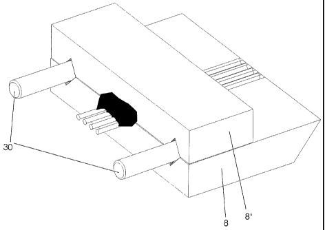
[0022] Fig. 1 is a 3D perspective view which shows four optical fibers;
[0023] Fig. 2 is a 3D perspective view which shows a first assembly which
comprises two alignment V-grooves (large grooves) in parallel with 2 dowel pin
V-grooves (large grooves) in parallel with four optical fiber v-grooves (small
grooves);
[0024] Fig. 3 is a 3D perspective view which shows a second assembly which
comprises two alignment V-grooves (large grooves) in parallel with 2 dowel pin
~5 V-grooves (large grooves);
[0025] Fig. 4 is a 3D perspective view of four optical fibers placed into the
small
v-grooves of the first assembly with a coating of transparent epoxy;
CA 02569263 2006-11-30
WO 2005/010587 PCT/CA2004/001084
_g_
[0026] Fig. 5 is a 3D perspective view of an intermediate assembly which
comprises an epoxy flattened using a cover plate (preferably glass) over the
first assembly of v-grooves and a second epoxy used to coat the tips of the
protruding optical fibers;
[0027] Fig. 6 is a 3D perspective view of the intermediate assembly where one
end is polished at a predetermined angle and the other end is polished flat;
[0028] Fig. 7 is a 3D perspective view which shows the intermediate assembly
where the glass plate has been removed and the remaining large surface is
polished flat;
[0029] Fig. 8 is a 3D perspective view which shows the insertion of the
alignment pins in their respective alignment v-grooves and the positioning of
the
second assembly over the first assembly using the alignment pins as reference;
[0030] Fig. 9 is 3D perspective view of the insertion of the external dowel
pins
into the dowel pin v-grooves to complete the ferrule assembly (as a male type
connector);
[0031] Fig. 10a is a 3D perspective view of an alternative embodiment to the
first ferrule that shows the temporary use of the external dowel pins to
locate
the second assembly before back polishing;
[0032] Fig. 10b is a 3D perspective view of an alternative embodiment to the
first ferrule that shows the removal of the external dowel pins and the
subsequent back polish of the connector side of the ferrule assembly;
[0033] Fig. 11 is a to-scale side view of the completed ferrule assembly
described in Fig. 9; '
[0034] Fig. 12 is a view of the connector side of the ferrule assembly showing
the internal alignment pins, the external dowel pins and the optical fibers
lying in
the same plane and the associated gap between first and second assembly;
CA 02569263 2006-11-30
WO 2005/010587 PCT/CA2004/001084
_g_
[0035] Fig. 13a is a 3D perspective front view of the ferrule assembly showing
the removal of only the cover plate to expose the optical fibers along their
respective v-grooves;
[0036] Fig. 13b is a 3D perspective front view of the ferrule assembly showing
the removal of the cover plate and an over-polish of the optical fibers along
one
side to expose and gain proximity to the optical core of the optical fibers;
[0037] Fig. 14 is a 3D perspective view of the first part of another
embodiment
of the invention;
[0038] Fig. 15 is a 3D perspective view of the second part of another
embodiment of the invention;
[0039] Fig. 16 is a 3D perspective view of the first part and the second part;
[0040] Fig. 17 is a 3D perspective view of the first part mating with the
second
part with a plurality of optical fibers;
[0041] Fig. 18 is a 3D perspective view of an intermediate assembly consisting
of the first part mated with the second part with a plurality of optical
fibers where
a bonding substance has been injected into the first and second parts;
[0042] Fig. 19 is a 3D perspective view of the intermediate assembly where one
end has been polished at a predetermined angle and the other end is polished
flat;
[0043] Fig. 20 is a 3D perspective view of the intermediate assembly where the
bottom surface has been polished flat to expose the optical fibers and dowel
pins are inserted into the back surface;
[0044] Fig. 21 is a to-scale side view of the completed second embodiment of
the invention as described in Fig. 20;
[0045] Fig. 22a is an end view of a single MM optical fiber before over-
polish;
CA 02569263 2006-11-30
WO 2005/010587 PCT/CA2004/001084
-10-
[0046] Fig. 22b is an end view of a single MM optical fiber after an 8.5
micron
over-polish;
[0047] Fig. 23 is a 3D perspective view of the cover plate showing the thin
layer
of wax (or other) material;
[0048] Fig. 24 is a 3D perspective view of the waxed cover plate placed over
the
first assembly which comprises two alignment V-grooves (large grooves) in
parallel with 2 dowel pin V-grooves (large grooves) in parallel with four
optical
fiber v-grooves (small grooves);
[0049] Fig. 25 is a front view of the optical fibers pressed into the v-
grooves
(small grooves) with the dark region representing the bonding epoxy and the
hatched region representing the wax;
[0050] Fig. 26 is a 3D perspective view of the waxed cover plate and the first
assembly where one end is polished at a predetermined angle;
[0051] Fig. 27 is a 3D perspective view of the angle polished first assembly
without the wax or waxed cover plate; and
[0052] Fig. 28 is a front view of the bevel optical fiber with two thick rays.
indicating how the tensing effect is produced using the curvature of the
optical
fiber.
It will be noted that throughout the appended drawings, like features are
identified by like reference numerals.
DETAILED DESCRIPTION OF THE PREFERRED EMBODIMENT
[0053] The parallel optical ferrule is a mechanical structure used to
interface
between a parallel optical fiber ribbon cable and an array of optoelectronic
devices, such as a vertical cavity surface emitting laser (VCSEL) array or
photodetector array.
[0054] The ferrule has two ends; one end interfaces with the optoelectronic
device and the other end interfaces with a standard connector assembly such
CA 02569263 2006-11-30
WO 2005/010587 PCT/CA2004/001084
-11-
as the MPO/MTPT"" parallel optical connector. Within the ferrule is a linear
array
of optical fibers that optically connects both ends of the ferrule.
[0055] The first end of the ferrule is polished at a 45-degree angle to create
a
reflective glass-air interface at the fiber tips. This interface can reflect
light at 90-
degrees by either total internal reflection (TIR) when the glass-air interface
is
preserved, or by depositing a reflective metal layer on the exposed tips of
the
fiber. The reflective metal layer may be made of gold, silver, etc. The use of
a
reflective layer allows for the OE component and ferrule to be provided with a
protective coating without interfering with the light coupling.
[0056] Light directed at the 45-degree tips of the optical fiber will be
reflected
and coupled into the optical fiber orthogonal to the initial direction. In
this
situation, light will pass though the side of the optical fiber, through the
cladding,
and reflect off the 45-degree tip, due to TIR or the metallic surface, into
the core
of the optical fiber. Conversely, when light is already in the core and
traveling
towards the 45-degree polished tip, it reflects off the 45-degree tip, due to
TIR
or the metallic surface, and is directed normal to the optical fiber passing
through the cladding and out of the side of the optical fiber.
[0057] The other end has a surface that can accept an end-coupled, or butt-
coupled, mating connector such as a standard flat-polished MPO/MTPTM
parallel optical connector. Preferably, the ferrule includes'2 positioning
dowel-
pins, one on either side of a linear array of optical fibers. The face of this
structure is polished to optical quality.
[0058] First preferred embodiment of the invention - silicon v-groove
[0059] The parallel optical ferrule is comprised of 8 elements, one of which
is
used as a sacrificial element and is not present in the final assembly. The
elements are described as: a first silicon v-groove chip, a second silicon v-
groove chip, 2 internal alignment dowel pins, 2 external mating dowel pins,
optically transparent epoxy, protective epoxy, parallel optical fiber ribbon,
and a
sacrificial cover plate.
CA 02569263 2006-11-30
WO 2005/010587 PCT/CA2004/001084
-12-
[0060] A parallel optical fiber ribbon (2) typically has several optical
fibers (6)
within protective polymer jackets (4) that keep them roughly pitched at 250-
microns, however this is not precise. The end portions, approximately 2-cm
long, of the protective polymer jackets of the optical fiber ribbon (6) are
stripped
and clean - using standard means - to produce 2-cm~ long segments of
separated parallel optical fibers (i.e.: only the glass), still roughly
pitched at 250-
microns but not touching each other. The segment of bare optical fiber remains
part of the ribbon cable, as shown in Figure 1.
[0061] The first silicon v-groove chip (8) in Figure 2 and second silicon v-
groove
chip (8') in Figure 3 are each chemically etched on one of their large
surfaces
to produce v-shaped grooves in the silicon. The chips are on the order of 1-cm
x
1-cm x 0.2-cm and 1-cm x 0.5-cm x 0.2-cm in size, respectively.
[0062] The process of creating v-grooves in crystalline silicon is well known
and
described in the literature. The v-groove structure is used in this case to
maintain four essential features for providing~a standard connector.
Preferably,
a first essential feature is that the optical fibers are pitched from each
other at
precisely 250-microns, a second essential feature is that the optical fibers
remain in precisely the same plane. Preferably, a third essential feature is
that
the axial center of the alignment dowel pins are located in the same plane as
the axial center of the optical fibers, and the fourth essential feature is
that the
dowel pins and optical fibers mate properly with standard parallel optical
connectors such as the MPO/MTPTM connector.
[0063] The large v-grooves in the first silicon v-groove chip (8) define the
position of the internal alignment dowel pin v-grooves (12a, 12b), the
position of
the external mating dowel pin v-grooves (10a, 10b) and the position of the
parallel optical fiber v-grooves (14) all relative to each other. Preferably,
the
dimensions of the parallel optical fiber v-grooves ensure that the optical
fibers
are completely inside their respective grooves and flush with the surface of
the
first silicon v-groove chip (to form a 3-point contact). Preferably, the
external
mating dowel pin v-grooves ensure that the axial centers of the external dowel
pins lie in the same plane as the axial centers of the optical fibers. The
external
CA 02569263 2006-11-30
WO 2005/010587 PCT/CA2004/001084
-13-
mating dowel pin v-grooves are located on the side of the chip where the
standard MTP/MPOT"" connector will be connected. The second silicon v-groove
chip (8'), shown in Figure 3, defines the position of the corresponding
internal
alignment dowel pin v-grooves (12a', 12b') and the position of the external
mating dowel pin v-grooves (10a', 10b').
[0064] Since the optical fibers in the optical fiber v-grooves of the first
silicon v-
groove chip are flush with the surface, their axial centers lie 62.5-microns
below
the surface. Therefore, the external mating dowel pin v-grooves on the first
silicon v-groove chip must be 62.5-microns deeper than those on the second
silicon v-groove chip. This arrangement maintains the axial centers of the
external mating dowel pins in the same plane as the axial centers of the
optical
fibers as shown in Figure 12. To reduce number of masking steps when making
the silicon v-grooves chips, the internal alignment pin v-grooves will
typically be
at the same depth as the external mating dowel pin v-grooves, but this does
not
have to be the case.
[0065] The first silicon v-groove chip, the optical fiber, and a small
quantity of
transparent optical epoxy (16) .are now assembled in Figure 4. The optical
fibers (6) are placed in the v-grooves with the ends protruding past the first
silicon v-groove chip (8), the other end still part of the ribbon cable.
[0066] A cover plate (18) is placed over the optical fibers in the v-grooves
and
pressed together to sandwich the optical fibers in place as shown in Figure 5.
The epoxy is then cured. The ends of the optical fibers are coated with a
small
amount of protective epoxy (20) to protect them during the polishing process.
Once this protective epoxy has hardened, the ribbon cable is broken away
leaving the sandwiched optical fiber protruding from both ends.
[0067] This intermediate ferrule is then placed on a polishing machine such
that
it is held at a 45-degree angle to the surface of the polisher with the corner
of
the first silicon v-groove chip polishing first and progressively towards the
cover
plate. This creates the 45-degree angled polish of the optical fibers (22) as
shown in Figure 6. The intermediate ferrule is then placed on a polishing
CA 02569263 2006-11-30
WO 2005/010587 PCT/CA2004/001084
-14-
machine such that the opposite side is polished flat (24) to create a flat
polish of
the optical fibers for the standard optical connector. However, this flat
polishing
step can be deferred till later in the process. Preferably, standard lapping
and
polishing techniques are applied, including progressively finer grits of
polishing
paper, correct timing, appropriate slurry mixtures, and a method of holding
the
parts in a rigid manner. A thin metallic coating can be applied to the 45-
degree
beveled surface to create a mirrored surface on the inside region of the
optical
fiber. The metallic coating can be made of gold, silver, etc. The rest of this
application will assume no metallic coating, but there is no difference to the
procedure if one is included at this point.
[0068] To remove the cover plate, several methods could be used. The cover
plate could be made of a material that would not adhere to the epoxy or
silicon
v-groove chip. The plate could then be mechanically removed after the epoxy
had secured the optical fibers in place. This may or may not result in a
suitable
optically flat surface, and polishing (buffing) still might be required. The
cover
plate might also be made of a material that could be chemically dissolved,
leaving the fibers, epoxy and glue unaffected. This also may or may not result
in
a suitable optically flat surface, and polishing (buffing) still might be
required.
[0069] The preferred method will assume that the cover plate is removed by
polishing. The intermediate assembly is then placed on a polishing machine
such that the large exposed surface of the cover plate is in contact with the
polishing surface. The cover plate is then lapped and polished until it has
been
completely worn away (26) leaving only the first silicon chip with optical
fibers
embedded in optical epoxy within the v-grooves, as shown in Figure 7. A
"perfect-polish" is obtained when the cover plate is entirely removed without
polishing the silicon chip to expose the optical fibers from the side (36) as
shown in Figure 13a.
[0070] However, during the polishing step to remove the cover plate, an "over-
polish" (38) can be applied to the surface. Over-polishing creates a flat side
along the outside the optical fibers in the v-grooves. This is advantageous
because it allows the light to be coupled closer to the core of the optical
fiber,
CA 02569263 2006-11-30
WO 2005/010587 PCT/CA2004/001084
-15-
resulting in higher coupling efficiency. The over-polish also allows a more
flexible tolerance during the polishing step; assuming a 1-cm x 1-cm~ surface
area silicon chip, a worst case tilt angle of 0.36-degrees in one direction
and
0.65-degrees in the other can exist over the optical fiber array before damage
to
the core results.
[0071] The second silicon v-groove chip (8') is now aligned to the first
silicon v-
groove chip (8) using the internal alignment dowel pins as shown in Figure 8.
A
small amount of epoxy is placed on the first silicon v-groove chip and the
internal alignment dowel pins (28) are placed in their respective grooves and
both chips are used to sandwich the dowel pins in place. A close-up view of an
internal alignment dowel pin in the internal alignment v-groove is shown in
Figure 12 and shows how the silicon chips contact the dowel pin in 4 locations
(34). This ensures that the external mating v-grooves of both the first and
second silicon v-groove chip are located at the proper position. Due to the
contact of the internal alignment dowel pins within their respective v-
grooves, a
small gap (32) exists between the flat polished surface of the first (8) and
second (8') silicon v-groove chips which further aids the process of "over-
polishing" by not requiring direct contact between the two chips.
[0072] Once the assembly in Figure 8 has been assembled, a flat polish of the
optical fibers on the standard optical connector side can be done (or done
again
- depending on the procedure above) before the external mating dowel pins (30)
are inserted. This provides an optical quality surface for mating with a
standard
optical connector such as the MPO/MTPT"". The external mating dowel pins can
be left out (for a female type ferrule) or inserted and glued (for a male type
ferrule) as shown in Figure 9.
[0073] Second preferred embodiment - molded plastic
[0074] The structure used to hold the optical fibers may be fabricated from
other
materials and other assembly methods could be used. The mechanical
structure that holds the optical fibers in the same plane and pitched 250-
microns from each other as well as the two dowel pins can be based on
CA 02569263 2006-11-30
WO 2005/010587 PCT/CA2004/001084
-16-
precision micro-molding techniques of plastic as described in the literature.
This
version of the parallel optical connector is comprised of 5 elements. The
elements are described as a first injection-molded plastic ferrule, a second
injection-molded plastic ferrule, epoxy, dowel pins, and parallel optical
fiber
ribbon.
[0075] The first injection-molded plastic ferrule (40) is on the order of 1-cm
x 1-
cm x 0.3-cm in size, as shown in Figure 14. It is a hollow plastic box with
the
back and top sides open (44). The front side has a linear array of 125-micron
diameter holes pitched at 250-microns (42). The holes bore into the plastic
approximately 0.05-cm and are used to align the tips of the optical fibers
(6).
Inside the box, a flat surface is used to keep the optical fibers equal or
higher
than the array of holes. The other interior sides of the box are tapered
towards
the array of holes to better guide the fibers into the holes during their
insertion.
[0076] The second injection-molded plastic ferrule (52) is shown in Figure 15
and is very similar to the first except that it is slightly larger, in order
to mate to
the first ferrule as shown in Figure 16. The second ferrule has two extra
dowel
pin holes (46) located on either side of the linear array of 125-micron
diameter
holes pitched at 250-microns (48). The dowel pin holes (46) are used ~ to mate
with standard optical connectors such as the MPO/MTPTM. One additional
characteristic of the second ferrule is that the array of 125-micron holes is
shifted laterally upwards with respect to the 125-micron holes of the first
ferrule.
This results in slightly bent optical fibers within the ferrule assembly, but
is
required so that the bottom surface can be polished flat and still accommodate
- the dowel pins as shown in Figure 21.
[0077] A parallel optical fiber ribbon (2) typically has several optical
fibers within
the same plastic coating that keep the fibers roughly pitched at 250-microns,
however this is not precise. The end portion, approximately 3-cm long, of the
optical fiber ribbon is stripped and cleaned of its plastic coating - using
standard
means - to produce a 2-cm long segment of separated parallel optical fibers
(i.e.: only the glass). The segment of bare optical fiber remains part of the
ribbon cable as shown in Figure 1.
CA 02569263 2006-11-30
WO 2005/010587 PCT/CA2004/001084
-17-
[0078] The array of bare optical fibers (6) is inserted into the front side of
the
second plastic ferrule and the back side of the first plastic ferrule as shown
in
Figure 17. The ferrules are pushed together with the optical fibers protruding
from both ends.
[0079] Epoxy (54) is then injected into the injection opening (44 and 50) and
the
optical fibers are pushed and pulled back and forth to ensure that the epoxy
has
well coated all the fibers within the array of holes. Epoxy is then applied to
the
outside of the arrays of holes where the optical fibers are protruding. The
epoxy
is then cured, by heat, time, or UV light, as shown in Figure 18.
[0080] The assembly is then placed on a polishing machine such that the front
facet of the first ferrule is held at a 45-degree angle to the surface of the
polisher (56). The corner of the front surface of the first ferrule is
polished until
the optical fibers are completely beveled at 45-degrees (60). The front
surface
of the second ferrule (which becomes the back surface of the completed
assembly), is also polished to produce a flat surface polish (58) suitable for
standard optical connectors such as the MPO/MTPTM, as shown in Figure 19.
[0081] Preferably, standard lapping and polishing techniques are applied,
including progressively finer grits of polishing paper, correct timing,
appropriate
slurry mixtures, and a method of holding the parts in a rigid manner.
[0082] It is at this point that a thin reflective metallic coating can be
applied to
the 45-degree beveled surface. The thin reflective metallic coating can be
made
of gold, silver, etc. The metal surface creates a mirror surface on the inside
region of the optical fiber. The rest of this document will assume no metallic
coating, but there is no difference to the procedure if one is included at
this
point.
[0083] The assembly is then placed on a polishing machine such that the larger
bottom surface (62) is in contact with the polishing surface. The bottom
surface
is lapped and polished until the longitudinal sides of the optical fibers have
been
exposed, as shown in Figure 22a. The over-polishing technique can now be
used to improve coupling efficiency by getting closer to the core of the
optical
CA 02569263 2006-11-30
WO 2005/010587 PCT/CA2004/001084
-18-
fibers. Furthermore, due to the typically opaque or poor optical quality of
the
plastic molded ferrule, the over-polishing technique is essentially required.
By
polishing into the plastic face by at least 8.5-microns (66), as shown in
Figure
22b, windows of the width of the multimode optical fiber core (68) can be
produced allowing the light to pass into the lateral side of the optical
fibers.
Over-polishing can be extended further into the plastic ferrule thereby
increasing the window opening to the optical fibers as long as the core is not
damaged. Single mode optical fiber can be handled in a similar manner
although the mechanical tolerances for the subcomponents must be tighter and
greater care in alignment precision must be used.
[0084] Finally, the dowel pins (64) are inserted into their respective holes
as
shown in Figure 20. The complete plastic ferrule is shown in profile in Figure
21.
[0085] Alternate Assembly Technique
[0086] Further to the method of removing the cover plate to expose the lateral
sides of the optical fiber, a method has been devised that uses a cover plate
(18) that has a thin layer of wax (Polyethylene Phthalate) (80) deposited on
it
Figure 23.
[0087] This wax melts at 120oC and is soluble in acetone. It is used primarily
to
mount samples for polishing and cross-sectioning and therefore withstands the
mechanical vibrations and stresses that are associated with lapping and
polishing. It is also a transparent, clear material and therefore can allow
light to
pass through it (for a sufficiently thin layer) to cure light-curing epoxy
below it if
required. The material also has a very slight malleability or softening as the
temperature increases towards 120oC. Note that any material that has the
same general properties as the wax could also be used.
[0088] The deposition of the wax on the cover plate can be done through a
variety of methods including spin-coating the hot wax on a large area
(typically
a glass microscope slide 1.3-mm thick) that can later be cut or snapped into
smaller pieces. The actual thickness of the wax is somewhat arbitrary but
CA 02569263 2006-11-30
WO 2005/010587 PCT/CA2004/001084
-19-
keeping it within 100-microns prove to be satisfactory. Flatness is a
requirement
and can be gauged by visual inspection. The size of the cover plate is
typically
slightly smaller than the size of the first assembly (silicon v-groove chip)
but is
completely covered on one side with the wax.
[0089] The optical fibers are loosely placed within their respective v-grooves
of
the first assembly (silicon v-groove chip). A thin layer of epoxy (82) (or,
more
generally, bonding material) is placed over and around the optical fibers in
the
v-grooves and all air bubbles above and below the optical fibers are worked-
out.
As shown in Figure 24, the waxed cover plate is then placed over the optical
fibers where it presses down into the optical fibers and v-grooves to squeeze
out some of the epoxy. The applied pressure need not be more than a
reasonable amount of force applied by hand. This is to ensure that the
somewhat malleable wax (80) is pushed into the two region above and to each
side of the optical fiber thereby pushing out any epoxy (82) that would have
been above the optical fiber as in Figure 25. The cover plate, the wax, the
optical fibers, the epoxy and the silicon v-groove chip form a layered
sandwich.
The epoxy can be UV-light cured through the cover plate and wax assuming
they are transparent or can be time cured. Note that transparency is not
essential, however it does allow the operator to see how the optical fibers
are
positioned at all times.
[0090] The same procedure for angle polishing the part described above can
then be used to produce the 45-degree bevel (84) as in Figure 26. The cover
plate, wax, optical fibers, epoxy and silicon v-groove chip will all polish
well
given appropriate diamond lapping films and cold water lubrication.
[0091] The removal of the waxed cover plate involves heating the assembly and
melting the wax. This procedure is ideally done as quickly as possible to
avoid
over-heating the epoxy or silicon and can usually be done in under 5 seconds
(assuming a 120oC hot plate is already turned on).
[0092] The remaining residual wax can be removed by gently agitating the
beveled end in acetone. Typical cleaning steps are then performed such as
CA 02569263 2006-11-30
WO 2005/010587 PCT/CA2004/001084
-20-
drag-and-drop cleaning of the front end of the first assembly using alcohol or
methanol and small quantities of compressed air to clean any residue from the
part. The resulting part as shown in Figure 27 is very similar to the above
procedure except that the original thickness of the silicon v-groove chip
remains
the same and the optical fibers have air spaces over and to the sides (86).
[0093] This procedure only requires one other polishing step to create a flat
back polish for the optical connector as described in a previous section. It
no
longer requires the removal of the cover plate by polishing. This reduces the
number of steps required and allows the optical fiber to act as a cylindrical
lens
as shown in Figure 28 to help increase the coupling efficiency and is
highlighted by the thicker lines representing ray-tracing (88).
[0094] It should be noted that the lens effect only acts to increase the
coupling
efficiency if the light source (90) (the object) is outside the effective
focal length
of the curvature of the optical fiber. Typically around 75-microns away from a
125-micron diameter optical fiber allows for highest coupling - although this
is
somewhat of a optical design issue for the intended system.
[0095] Applications
[0096] The parallel optical ferule may be used in applications involving the
direct
coupling of light from a micro-laser, such as a VCSE~, into an optical fiber.
Conversely, coupling light out of an optical fiber onto a photodetector, such
as a
PIN diode, can also be done. The parallel optical ferule may also be used to
couple light into optical elements such as a micro-lens array.
[0097] Although the previous embodiments do not specify the use of multimode
or single mode optical fiber, the physical structure of the previous
embodiments
imply the use of a relative large optical target such as a multimode optical
fiber
core of 62.5-microns. In this application where a lens structure is used, a
smaller target, such as a single-mode optical fiber core of only 8-microns
(effective field diameter), is possible. The lens structure focuses the light
into a
smaller spot closer to the diameter of the single-mode optical fiber core.
CA 02569263 2006-11-30
WO 2005/010587 PCT/CA2004/001084
-21 -
[0098] The embodiments of the invention described above are intended to be
exemplary only. The scope of the invention is therefore intended to be limited
solely by the scope. of the appended claims.