Note: Descriptions are shown in the official language in which they were submitted.
CA 02569349 2006-11-30
WO 2006/078293 PCT/US2005/017839
METHOD OF MAKING AN APPLICATOR LIQUID
FOR ELECTRONICS FABRICATION PROCESS
Cross-Reference to Related Applications
[0001] This application is related to the following applications, all of which
are
assigned to the assignee of this application, and all of which are
incorporated by reference
in their entirety: Nanotube Films and Articles (U.S. Patent No. 6706402) filed
April 23,
2002; Methods of Nanotube Films and Articles (U.S. Patent Appl. No. 10/128117)
filed
April 23, 2002; and Patterning of Nanoscopic Articles (U.S. Provisional Patent
Appl. No.
601501033) filed on September 8, 2003.
Background
1. Technical Field
[0002] This invention describes spin-coatable liquids for use in the
preparation of
nanotube films. Such liquids are used in creating films and fabrics of
nanotubes or
mixtures of nanotubes and other materials on a variety of substrates including
silicon,
plastics, paper and other materials. Tn particular, the invention describes
spin-coatable
liquids containing nanotubes for use in electronics fabrication processes.
Furthermore,
the spin-coatable liquids meet or exceed specifications for a semiconductor
fabrication
facility, including a class 1 environment.
2. Discussion of Related Art
[0003] Nanotubes are useful for many applications; due to their electrical
properties
nanotubes may be used as conducting and semi-conducting elements in numerous
electronic elements. Single walled carbon nanotubes (SWNTs) have emerged in
the last
decade as advanced materials exhibiting interesting electrical, mechanical and
optical
properties. However, the inclusion or incorporation of the SWNT as part of
standard
CA 02569349 2006-11-30
WO 2006/078293 PCT/US2005/017839
microelectronic fabrication process has faced challenges due to a lack of a
readily
available application method compatible with existing semiconductor equipment
and
tools and meeting the stringent materials standards required in the electronic
fabrication
process. Standards for such a method include, but are not limited to, non-
toxicity, non-
flammability, ready availability in CMOS or electronics grades, substantially
free from
suspended particles (including but not limited to submicro- and nano-scale
particles and
aggregates), and compatible with spin coating tracks and other tools currently
used by the
semiconductor industry.
[0004] Individual nanotubes may be used as conducting elements, e.g. as a
channel in
a transistor, however the placement of millions of catalyst particles and the
growth of
millions of properly aligned nanotubes of specific length presents serious
challenges.
United States Patent Nos. 6,643,165 and 6,574,130 describe electromechanical
switches
using flexible nanotube-based fabrics (nanofabrics) derived from solution-
phase coatings
of nanotubes in which the nanotubes first are grown, then brought into
solution, and
applied to substrates at ambient temperatures. Nanotubes may be derivatized in
order to
facilitate bringing the tubes into solution, however in uses where pristine
nanotubes are
necessary, it is often difficult to remove the derivatizing agent. Even when
removal of
the derivatizing agent is not difficult, such removal is an added, time-
consuming step.
[0005] There have been few attempts to disperse SWNTs in aqueous and non-
aqueous solvents. Chen et al. first reported solubilization of shortened, end-
functionalized SWNTs in solvents such as chloroform, dichloromethane,
orthodichlorobenzene (ODCB), CS2, dimethyl formamide (DMF) and tetrahydrofuran
(THF). See, "Solution Properties of Single-Walled Nanotubes", Science 1998,
282, 95-
98. Ausman et al. reported the use of SWNTs solutions using sonication. The
solvents
used were N-methylpyrrolidone (NMP), DMF, hexamethylphosphoramide,
2
CA 02569349 2006-11-30
WO 2006/078293 PCT/US2005/017839
cyclopentanone, tetramethylene sulfoxide and E-caprolactone (listed in
decreasing order
of carbon nanotube solvation). Ausman at e1. generally conclude that solvents
with good
Lewis basicity (i.e., availability of a free electron pair without hydrogen
donors) are good
solvents for SWNTs. See, "Organic Solvent Dispersions of Single-Walled Carbon
Nanotubes: Toward Solutions of Pristine Nanotubes", J. Phys. Chem. B 2000,
104, 8911.
Other early approaches involved the fluorination or sidewall covalent
derivatization of
SWNTs with aliphatic and aromatic moieties to improve nanotube solubility.
See, e.g., E.
T. Mickelson et al., "Solvation of Fluorinated Single-Wall Carbon Nanotubes in
Alcohol
Solvents", J. Phys. Chem. B 1999, 103, 4318-4322.
[0006] Full-length soluble SWNTs can be prepared by ionic functionalization of
the
SWNT ends dissolved in THF and DMF. See, Chen et al., "Dissolution of Full-
Length
Single-Walled Carbon Nanotubes", J. Phys. Chem. B 2001, 105, 2525-2528 and J.
L.
Bahr et al Chem. Comm. 2001, 193-194. Chen et al. used HiPCOTM as-prepared
(AP)-
SWNTs and studied a wide range of solvents. (HiPCOTM is a trademark of Rice
University for SWNTs prepared under high pressure carbon monoxide
decomposition).
The solutions were made using sonication.
[0007] Bahr et al. ("Dissolution Of Small Diameter Single-Wall Carbon
Nanotubes In
Organic Solvents?", Chem. Commun., 2001, 193-194) reported the most favorable
solvation results using ODCB, followed by chloroform, methylnaphthalene,
bromomethylnaphthalene, NMP and DMF as solvents. Subsequent work has shown
that
good solubility of AP-SWNT in ODCB is due to sonication-induced polymerization
of
ODCB, which then wraps around SWNTs, essentially producing soluble polymer
wrapped (PW)-SWNTs. See Niyogi et al., "Ultrasonic Dispersions of Single-
Walled
Carbon Nanotubes", J. Phys. Chem. B 2003, 107, 8799-8804. Polymer wrapping
usually
affects sheet resistance of the SWNT network and may not be appropriate for
electronic
3
CA 02569349 2006-11-30
WO 2006/078293 PCT/US2005/017839
applications where low sheet resistance is desired. See, e.g., A. Star et al.,
"Preparation
and Properties of Polymer-Wrapped Single-Walled Carbon Nanotubes", Angew.
Chem.
Int. Ed. 2001, 40, 1721-1725 and M. J. O'Connell et al., "Reversible Water-
Solubilization
Of Single-Walled Carbon Nanotubes By Polymer Wrapping", Chem. Phys. Lett.
2001,
342, 265-271.
[0008] While these approaches were successful in solubilizing the SWNTs in a
variety of organic solvents to practically relevant levels, all such attempts
resulted in the
depletion of the ~ electrons that are essential to retain interesting
electrical and optical
properties of nanotubes. Other earlier attempts involve the use of cationic,
anionic or
non-ionic surfactants to disperse the SWNT in aqueous and non-aqueous systems.
See,
Matarredona et al., "Dispersion of Single-Walled Carbon Nanotubes in Aqueous
Solutions of the Anionic Surfactant", J. Phys. Chem. B 2003, 107, 13357-13367.
While
this type of approach has helped to retain the electrical conductivity and
optical properties
of the SWNTs, most such methods leave halogens or alkali metals or polymeric
residues,
which tend to severely hamper any meaningful use in microelectronic
fabrication
facilities.
[0009] There is a need for a method of solvating or dispensing nanotubes in
solvents
for use in electronics applications. There remains a further need for methods
that meet the
criteria outlined above for low toxicity, purity, cleanliness, ease of
handling and
scalability.
4
CA 02569349 2006-11-30
WO 2006/078293 PCT/US2005/017839
Summary of tlae Invention
[0010] One aspect of the present invention is directed to a method of making
an
applicator solution containing nanotubes for use in an electronics fabrication
process.
The level of particulate and metallic impurities is controlled in the
applicator liquid so
that the applicator liquid satisfies preselected processing requirements.
[0011] A composition of nanotubes for use in an electronics fabrication
process
includes a liquid medium containing a plurality of nanotubes pretreated to
reduce the
level of metal and particulate impurities to a preselected level. The solvents
are present at
commercially meaningful levels, e.g., the nanotubes are at a concentration of
greater than
1 mg/L. The nanotubes are homogeneously distributed in the liquid medium
without
substantial precipitation or flocculation.
[0012] According to one aspect of the invention, a method of making an
applicator
liquid containing nanotubes for use in an electronics fabrication process
includes
characterizing an electronic fabrication process according to fabrication
compatible
solvents and allowable levels of metallic and particle impurities; providing
nanotubes that
satisfy the allowable impurities criteria for the electronics fabrication
process; providing a
solvent that meets the fabrication compatible solvents and allowable
impurities criteria
for the electronic fabrication process; and dispersing the nanotubes into the
solvent at a
concentration of at least one milligram of nanotubes per liter solvent to form
an applicator
liquid.
[0013] In another aspect of the invention, a method of making a high purity
nanotube
article includes depositing nanotubes onto a surface from a nanotube
composition
comprising a plurality of nanotubes in a solvent, in which the nanotube
composition is
substantially free of metallic and/or carbonaceous impurities.
CA 02569349 2006-11-30
WO 2006/078293 PCT/US2005/017839
[0014] The fabrication processes can have varying requirements for solvent and
raw
material composition and purity. According to one aspect of the present
invention,
nanotube films of varying composition and purity are obtained in these
fabrication
processes having varying processing specifications and environmental
requirements.
[0015] According to one aspect of the present invention, nanotube films having
high
standards of non-toxicity and purity are provided. Such films may be
fabricated in
semiconductor fabrication processes, for example, CMOS and advanced logic and
memory fabrications. Such fabrication processes may produce devices having
fine
features, e.g., < 250 nm.
[0016] According to other aspects of the present invention, nanotube films
having less
stringent standards for chemical composition and purity are provided. Such
nanotube
films include those fabricated, for example, using interconnect fabrication
and fabrication
of chemical and biological sensors.
Brief Description of the Drawing
[0017] The invention is described with reference to the Drawing, which is
presented
for the purpose of illustration only and which is not intended to be limiting
of the
invention.
[0018] Figure 1 illustrates a typical scanning electron micrograph (SEM) of an
unpurified nanotube fabric; and
[0019] Figure 2 illustrates a typical SEM image of a purified nanotube fabric.
Detailed Description of the Inventio~a
[0020] Nanotubes have been the focus of intense research efforts into the
development of applications that take advantage of their electronic,
biological, andlor
6
CA 02569349 2006-11-30
WO 2006/078293 PCT/US2005/017839
material properties. In one or more embodiments, a spin-coatable liquid
containing a
controlled concentration of purified nanotubes is prepared in a liquid medium.
The spin-
coatable liquid may be used to create nanotube films and fabrics of
substantially uniform
porosity. Certain embodiments provide spin-coatable liquids having a purity
level that is
commensurate with the intended application. Other applications provide spin-
coatable
liquids meeting or exceeding specifications for class 1 semiconductor
fabrication.
[0021] In one or more embodiments, a nanotube composition includes a liquid
medium containing a mixture of single-walled or multi-walled nanotubes that is
stable
enough for certain intended applications, such as spin coating in a class 1
production
facility. The nanotubes in the nanotube composition remain suspended,
dispersed,
solvated or mixed in a liquid medium without substantial precipitation,
flocculation or
any other macroscopic interaction that would interfere with the ability to
apply the
nanotube solution to a substrate and form a uniform porosity. If there were
significant
precipitation or aggregation of the nanotubes, the nanotubes would clump
together and
form non-uniform films, which would be undesirable. The nature by which the
nanotubes
interact with the solvent to form a stable composition is not limited. Thus,
for example,
the nanotubes may be suspended or dispersed in the solvent or they may be
solvated or
solubilized in the solvent. The stable nanotube composition typically forms a
homogeneous distribution of nanotubes in the solvent.
[0022] At the present time, it is desirable that the nanotubes remain
distributed in the
solvent medium without substantial precipitation, flocculation or other
macroscopic
interaction, for at least one hour, or for at least 24 hours, or even for at
least one week.
Substantial precipitation and flocculation and the like can be detected by a
variety of
methods. Precipitates and aggregates can be detected by visual inspection.
Alternatively,
precipitation or flocculation can be detected by analytical techniques, such
light scattering
7
CA 02569349 2006-11-30
WO 2006/078293 PCT/US2005/017839
or absorbance, or by observation of nanotubes once they are deposited on a
substrate from
the nanotube solution. A stable nanotube composition can exhibit prolonged
suspension
(typically several weeks to few months) of the SWNT in the medium with little
or no
detectable change in the scattered light intensity, or absorbance at a given
wavelength, or
viscosity.
[0023] Light scattering is measured using a monochromatic beam of light
traveling
through the solution. A change of light scattering intensity over time is
recorded usually
by a detector placed normal to the beam direction or from multiple detectors
placed at
various angles including the right angle. Another indicator especially at low
concentrations of SWNT is the fall in absorbance (at a given wavelength) as
function of
time. For higher concentrations of the solution, between the semidilute and
nematic
regimes, precipitation of individually suspended tubes leads to a noticeable
fall in the
viscosity of the suspension. Other methods of determining the stability of a
nanotube
composition for its intended purpose will be apparent to those of skill in the
art.
[0024] The nanotubes used in one or more embodiments of the present invention
may
be single walled nanotubes or multi-walled nanotubes and may be of varying
lengths.
The nanotubes may be conductive, semiconductive or combinations thereof.
Conductive
SWNTs are useful in the manufacture of nanotube films, articles and devices
and can be
used in the nanotube solutions according to one or more embodiments of the
invention.
Thus, the nanotube composition is integratable into current electronic
fabrication
processes including, by way of example, CMOS, bipolar-transistor, advanced
memory
and logic device, interconnect device, and chemical and biological sensor
fabrications.
[0025] In selecting a solvent for the nanotube composition, the intended
application
for the nanotube composition is considered. The solvent meets or exceeds
purity
specifications required in the fabrication of intended application. The
semiconductor
8
CA 02569349 2006-11-30
WO 2006/078293 PCT/US2005/017839
manufacturing industry demands adherence to the specific standards set within
the
semiconductor manufacturing industry for ultra-clean, static-safe, controlled
humidity
storage and processing environments. Many of the common nanotube handling and
processing procedures are simply incompatible with the industry standards.
Furthermore,
process engineers resist trying unfamiliar technologies. According to one
aspect of the
present invention, a solvent for use in a nanotube composition is selected
based upon its
compatibility or compliance with the electronics and/or semiconductor
manufacturing
industry standards.
[0026] Exemplary solvents that are compatible with many semiconducting
fabrication
processes, including but not limited to CMOS, bipolar, biCMOS, and MOSFET,
include
ethyl lactate, dimethyl sulfoxide (DMSO), monomethyl ether, 4-methyl -2
pentanone, N-
methylpyrrolidone (NMP), t-butyl alcohol, methoxy propanol, propylene glycol,
ethylene
glycol, gamma butyrolactone, benzyl benzoate, salicyladehyde, tetramethyl
ammonium
hydroxide and esters of alpha-hydroxy carboxylic acids. In one or more
embodiments,
the solvent is a non-halogen solvent, or it is a non-aqueous solvent, both of
which are
desired in certain electronic fabrication processes. In one or more
embodiments, the
solvent disperses the nanotubes to form a stable composition without the
addition of
surfactants or other surface-active agents.
[0027] In one aspect of the invention, nanotube compositions include a
plurality of
single-walled or mufti-walled nanotubes in ethyl lactate as the solvent. Ethyl
lactate is
one among the common solvent systems used by the electronics and electronic
packaging
industry and is an industry-accepted solvent that meets the industry standards
for safety
and purity. Ethyl lactate is available as a high purity solvent, or it can be
purified to
acceptable purity levels. Ethyl lactate has surprisingly been shown to exhibit
excellent
solubilizing capabilities for nanotubes. Furthermore, ethyl lactate can form
stable
9
CA 02569349 2006-11-30
WO 2006/078293 PCT/US2005/017839
nanotube compositions even in the presence of significant levels of
impurities, thereby
providing a versatile solution for application for formation of nanotube films
and fabrics
in a variety of applications. In one or more embodiments of the present
invention, a
nanotube solution of SWNT in ethyl lactate is provided. Purified SWNTs can be
solubilized in ethyl lactate at high concentrations, e.g., 100 mg/L, or even
higher.
Nanotube compositions include nanotubes homogeneously distributed in ethyl
lactate
without significant precipitation or flocculation.
[0028] Typical nanotube concentrations range from about 1 mg/L to 100 g/L, or
from
about 1 mg/L to lg/L, or about 10 mg/L, or about 100 mg/L, or even about 1000
mg/L
with a common concentration used for memory and logic applications of 100
mg/L. Such
a concentration is exemplary various useful concentrations ranges depend upon
the
application. For example in the case where a monolayer fabrics is desired one
could use a
less concentrated composition with a single or a few applications of the
nanotube
composition, e.g., by spin coating, to the substrate. In the event that a
thick multilayer
fabric is desired, a spraying technique could be employed with a nearly
saturated
nanotube composition. The concentration is, of course, dependent upon the
specific
solvent choice, method of nanotube dispersion and type of nanotube used, e.g.,
single-
walled or multiwalled.
[0029] Nanotubes may be prepared using methods that are well known in the art,
such
as for example, chemical vapor deposition (CVD) or other vapor phase growth
techniques
(electric-arc discharge, laser ablation, etc.). Nanotubes of varying purity
may also be
purchased from several vendors, such as Carbon Nanotubes, Inc., Carbolex,
Southwest
Nanotechnologies, EliCarb, Nanocyl, Nanolabs, and BuckyUSA (a more complete
list of
carbon nanotube suppliers is found at
http://www.cus.cam.ac.uk/~cs266llist.html).
Vapor-phase catalysts are typically used to synthesize nanotubes and, as a
result, the
CA 02569349 2006-11-30
WO 2006/078293 PCT/US2005/017839
nanotubes are contaminated with metallic impurities. Furthermore, formation of
nanotubes may also be accompanied by the formation of other carbonaceous
materials,
which are also a source of impurities in the nanotubes.
[0030] In one or more embodiments of the present invention, metallic particles
and
amorphous carbon particles are separated from nanotubes. The purification
process
reduces alkali metal ions, halogen ions, oligomers or polymers as active or
inactive
chemical components as part of the SWNT solution. The nanotube solutions
according to
certain embodiments of the present invention are substantially free of high
levels of these
particulate and/or insoluble materials (as well as other soluble materials
that are
incompatible with the semiconducting fabrication process). The nanotube
solutions are
thus purified for use in CMOS processing or other semiconducting fabrication
process.
[0031] Appropriate purification techniques desirably remove impurities without
affecting the nanotube chemical structure or electronic properties. Impurities
may be
removed for example, by dispersing the nanotubes in dilute acid solution to
dissolve
metal impurities, followed by separation of the nanotubes from the metallic
solution. A
mild acid treatment with nitric acid or hydrochloric acid may be used. Other
suitable
methods for metal removal include magnetic purification. Amorphous carbon may
be
removed, for example, by a combination of high speed centrifugation using an
ultracentrifuge and filtration techniques for example but not limited to
gravity filtration,
cross flow filtration, vacuum filtration and others. Other suitable
purification techniques
include the preferential oxidation of non-fullerenic carbonaceous materials.
Multiple
purification steps may be desired in order to obtain nanotubes of a purity for
use in a
CMOS-grade nanotube solution. See, for example, Chiang, et al., J. Phys.ChemB
105,
1157 (2001); and Haddon, et al., MRS Bulletin, April 2004)
11
CA 02569349 2006-11-30
WO 2006/078293 PCT/US2005/017839
[0032] In one or more embodiments, nanotubes are pretreated to reduce the
metallic
impurity levels to preselected levels.
[0033] In one or more embodiments, the nanotubes composition contains less
than
about 1018 atomslcm3 of metal impurities, or less than about 1016 atoms/cm3 of
metal
impurities, or less than about 1014 atoms/cm3 of metal impurities, or less
than about 1012
atoms/cm3 of metal impurities, or less than about 101° atoms/cm3 of
metal impurities.
Compositions having lower levels of metallic impurities, e.g. ca. 101° -
1012 atoms/cm3,
may be used in the manufacture of advanced devices having fine features, for
example,
devices having features of less than or equal to 250 nm.
[0034] Heavy metals, for examples metals having a specific gravity of 5 g/ml,
are
generally toxic in relatively low concentrations to plant and animal life and
tend to
accumulate in the food chain. Examples include lead, mercury, cadmium,
chromium, and
arsenic. Such compounds are carefully regulated in the semiconductor
fabrication
industry and are desirably maintained at minimum levels. In one or more
embodiments,
the nanotube composition includes less than about 1018 atomsfcm~ of heavy
metal
impurities, or less than about 1016 atomslcm3 of heavy metal impurities, or
less than about
1014 atomslcm3 of heavy metal impurities, or less than about 1012 atoms/cm3 of
heavy
metal impurities or even less than about 15 x 101° atoms/cm3 of heavy
metal impurities.
[0035] Similarly, the concentration of group I and group II elements is
regulated due
to the deleterious effect of elements such as sodium, potassium, magnesium and
calcium,
and the like, on the performance characteristics of the electronic device. In
one or more
embodiments, the nanotube composition includes less than about 1018 atoms/cm3
of group
I and group II element impurities, or less than about 1016 atoms/cm3 of group
I and group
II element impurities, or less than about 1014 atoms/cm3 of group I and group
II element
12
CA 02569349 2006-11-30
WO 2006/078293 PCT/US2005/017839
impurities, or less than about 1012 atomslcm3 of group I and group II element
impurities
or even less than about 15 x 101° atoms/cm3 of group I and group II
element impurities.
[003.6] Lastly, transition metals are also avoided due to their ready
migration and the
deleterious effect of such migration to the device performance. See, Mayer, et
al.
Electronic Materials Science: For Integrated Circuits in Si and GaAs, 2nd Ed,
Macmilliam, New York, 1988. As is the case for heavy metals and group I and
group II
metals, it is desired to maintain the impurity level of transition metals,
such as copper,
iron, cobalt, molybdenum, titanium and nickel, to less than preselected
values. In one or
more embodiments of the present invention, the nanotube composition includes
less than
about 1018 atoms/cm3 of transition metal impurities, or less than about 1016
atoms/cm3 of
transition metal impurities, or less than about 1014 atoms/cm3 of transition
metal
impurities, or less than about 1012 atoms/cm3 of transition metal impurities
or even less
than about 15 x 101° atoms/cm3 of transition metal impurities.
[0037] The impurity content of the nanotubes can be monitored using
conventional
methods, such as transmission electron microscopy (TEM) and scanning electron
microscopy (SEM) and using analytical techniques such as x-ray microanalysis
(EDAX),
or Vapor Phase Decomposition and Inductively-Coupled Plasma Mass Spectrometry
(VPD, ICP/MS).
[0038] Metallic impurity levels may be measured using conventional methods
such as
EDAX and VPD, IPC/MS. If large quantities of solution (e.g., > about 1000 mL),
are
available for testing, direct volumetric concentration measurements
(atoms/cm3) can be
determined. Alternatively, a known volume of the composition may be deposited
over a
known surface area and the surface impurity concentration (atoms/cm2) can be
determined.
13
CA 02569349 2006-11-30
WO 2006/078293 PCT/US2005/017839
[0039] In other embodiments of the present invention, nanotubes are pretreated
to
reduce the particulate impurities levels to a preselected level. The
semiconductor
industry has established standardized particulate impurity levels for
particular processes,
and the nanotubes may be pretreated to reduce the nanotube particulate levels
to below
the accepted levels. In one or more embodiments, the composition is
substantially free of
particle impurities having a diameter of greater than about 5 micron (gym), or
about 1 ~,m,
or about 3 hum, or about 500 nm, or 300 nm, or 100 nm, or even 45 nm.
[0040] Guidelines for particulate and metal impurity levels are found in the
International Technology Roadmad for Semiconductors (ITRS Roadmap). For
example,
the TTRS Roadmap states that at the 65 nm DRAM 1/a pitch, the critical
particle size is 33
nm and only 1 particle/m3 is allowed over the critical size. From the TTRS
2002 update,
at the 90 nm DRAM 1/a pitch node, the critical particle size is 45 nm with
only 2
particles/m3 allowed above the critical particle dimension. The ITRS Roadmap
for 90nm
DRAM 1/a pitch mode allows for <15 x101° atoms/cm3 of metal
contamination during
fabrication. Liquid chemicals utilized for wafer fabrication may contribute
<10
particles/mL of surface contamination. Other fabrication specifications may be
identified
by the TTRS.
[0041] The semiconductor industry has well-established testing protocols for
monitoring the particulate levels at, for example, 5 ~,m, 3 ~,m, 1 Vim, 500
nm, 300 nm and
100 nm. The metrology employed for detecting the particulate contaminate will
have a
resolution of 0.2 nm. Typical equipment include KLA Tencor surfscanTM and the
like.
Such testing methods and equipment may be readily adapted for use in
evaluating the
particulate levels of nanotube compositions.
[0042] In one or more embodiments of the present invention, the nanotube
composition is a homogeneous mixture of purified single walled carbon
nanotubes in
14
CA 02569349 2006-11-30
WO 2006/078293 PCT/US2005/017839
ethyl lactate at concentrations high enough to be useful in practical
applications in the
electronics industry, e.g., >_ 10 mg/L. The nanotube composition can be
electronics-grade
purity. In some embodiments, nanotubes purified to an impurity content of less
than 0.2
wt%, or less than 0.1 wt% free metal are solubilized in electronics-grade
ethyl lactate or
other suitable solvent.
[0043] It has been surprisingly discovered that nanotubes that have been
pretreated to
reduce the metallic and particulate impurity levels to below preselected
levels, such as
described herein, can form stable nanotube dispersions in a variety of
solvents.
Nanotubes, by way of example, SWNTs, and further by way of example purified
SWNT,
may be solubilized by dispersion in the appropriate solvent. One or more steps
of grind
or agitating the nanotubes in the selected solvent and sonication may enhance
solubilization.
[0044] The solution is appropriate for use as a spin-on SWNT solution for
electronic
and electronic packaging applications. The inventors envision that the
addition of various
optional additives may be useful to facilitate long term storage and
stabilization properties
of carbon nanotube solutions. Such additives include, but are not limited to
stabilizers,
surfactants and other chemicals known or accepted as additives to solutions
used for
fabrication of electronics. The nanotube solution according to one or more
embodiments
of the present invention and the methods of making the solution of nanotubes
have been
standardized for CMOS compatibility as required in conventional semiconductor
fabrication systems, i.e. the chemicals, spin coating tracks and other related
machineries
necessary to create the solutions of the present invention may be found in
typical CMOS
processing facilities or more generally may be present in many types of
services common
to the electronics industry including fabrication and packaging facilities.
CA 02569349 2006-11-30
WO 2006/078293 PCT/US2005/017839
[0045] The nanotube composition can be placed or applied on a substrate to
obtain a
nanotube film, fabric or other article. A conductive article includes an
aggregate of
nanotubes (at least some of which are conductive), in which the nanotubes
contact other
nanotubes to define a plurality of conductive pathways in the article. The
nanotube fabric
or film desirably has a uniform porosity or density. In many applications, the
nanotube
fabric is a monolayer.
[0046] Many methods exist for the application procedure including spin
coating,
spray coating, dipping and many others known for dispersing solutions onto
substrates.
For thicker fabrics beyond a monolayer, more applications or more concentrated
solutions
may be required. In fact.other techniques for application of the fabric may be
required as
has been outlined elsewhere (See Nanotube Films and Articles (U.S. Pat. No.
6,706,402)
filed April 23, 2002 and Methods of Nanotube Films and Articles (U.S. Pat.
Appln. No.
10/128117) filed April 23, 2002).
[0047] In one aspect of the invention, a highly purified nanotube article is
provided.
The article contains a network of contacting nanotubes for form pathway
through the
article. The nanotube network may form a ribbon or non-woven fabric. The
article
contains less than 0.2 wt% or 0.1 wt% free metal, or even less.
[0048] In one or more embodiments, the nanotubes article contains less than
about
1018 atoms/cm2 of metal impurities, or less than about 1016 atoms/cm2 of metal
impurities,
or less than about 1014 atoms/cm2 of metal impurities, or less than about 1012
atoms/cm2 of
metal impurities, or less than about 101° atoms/cm2 of metal
impurities. Compositions
having lower levels of metallic impurities, e.g. ca. 101° -1012
atoms/cm2, may be used in
the manufacture of advanced devices having fine features, for example, devices
having
features of less than or equal to 250 nm.
16
CA 02569349 2006-11-30
WO 2006/078293 PCT/US2005/017839
[0049] Heavy metals, for examples metals having a specific gravity of 5 g/ml,
are
generally toxic in relatively low concentrations to plant and animal life and
tend to
accumulate in the food chain. Examples include lead, mercury, cadmium,
chromium, and
arsenic. Such compounds are carefully regulated in the semiconductor
fabrication
industry and are desirably maintained at minimum levels. In one or more
embodiments,
the nanotube article includes less than about 1018 atoms/cm2 of heavy metal
impurities, or
even less than about 15 x 101° atoms/cm2 of heavy metal impurities.
[0050] Similarly, the concentration of group I and group II elements is
regulated due
to the deleterious effect of elements such as sodium, potassium, magnesium and
calciuriz,
and the like, on the performance characteristics of the electronic device. In
one or more
embodiments, the nanotube article includes less than about 1018 atoms/cm2 of
group I and
group II element impurities, or even less than about 15 x 101°
atoms/cm2 of group I and
group II element impurities.
[0051] Lastly, transition metals are also avoided due to their ready migration
and the
deleterious effect of such migration to the device performance. As is the case
for heavy
metals and group I and group II metals, it is desired to maintain the impurity
level of
transition metals, such as copper, iron, cobalt, molybdenum, titanium, and
nickel, to less
than preselected values. In one or more embodiments of the present invention,
the
nanotube article includes less than about 1018 atoms/cm2 of transition metal
impurities, or
even less than about 15 x 101° atoms/cm2 of transition metal
impurities.
[0052] The use of the term "about" reflects the variation that occurs in
measurement
and can range up to 30% of the measured value. For example, when determining
metal
impurity levels using VPD ICP-MS, the accuracy of the measurement is related
to the
precision of analytical signals, the recovery of trace metals from the wafer
surface, and
the accuracy of the standards used. Overall accuracy of the VPD ICP-MS
technique
17
CA 02569349 2006-11-30
WO 2006/078293 PCT/US2005/017839
varies from ~15%, at concentration levels higher than 10 times above the
method
detection limit, to ~30% or higher at concentration levels lower than 10 times
the
detection limits. Similar variability is expected in other measurements.
[0053] The following example are provided to illustrate the invention, which
is not
intended to be limiting of the invention, the scope of which is set forth in
the claims
which follow.
EXAMPLE 1
[0054] This example describes the purification of nanotubes.
[0055] Single-walled carbon nanotubes (SWNTs) were purified by stirring in
7.7M
HN03 for 8h followed by refluxing at 125°C for 12h. The acid refluxed
material was
washed with DI water three times by a sonication-centrifugation-decantation
cycle. The
DI water washed material was then vacuum filtered over a 5 micron filter until
a dried
SWNT membrane was obtained on the filter paper. This purified SWNT material
was
collected and used for making a SWNT composition.
EXAMPLE 2
[0056] This example describes the preparation of a nanotube composition and a
nanotube article.
[0057] In order to avoid recontamination of the nanotubes, clean room
conditions, for
example, Class 100 or greater, were maintained during preparation and
processing of the
nanotube composition. Twenty-one mg of single-walled nanotubes (SWNTs),
purified as
described above in Example 1 were soaked in 10 mL ethyl lactate (electronics
grade-
Sigma), ground with a mortar and pestle, sonicated and centrifuged to remove
the
supernatant. These steps were repeated as necessary to solubilize the carbon
nanotubes.
The solubilized nanotubes had a final concentration of 21 mg carbon nanotubes
per
18
CA 02569349 2006-11-30
WO 2006/078293 PCT/US2005/017839
250mL ethyl lactate, and the optical density at 550 nm of the solution was
measured to be
1.001.
[0058] Each individual step of the solubilization process is detailed in the
Table 1 for
the solubilization of SWNTs in ethyl lactate (EL). This protocol is
illustrative of one
means of forming a solubilized nanotube solution. Many other methods of
forming such
a solution are possible by adding or subtracting steps involving agitation and
solubilization depending upon the specific requirements for concentration,
solution
stability and ultimate performance metrics of the desired fabric.
19
CA 02569349 2006-11-30
WO 2006/078293 PCT/US2005/017839
TABLE 1: Process Flow Chart for SWNT solubilization in Ethyl-Lactate
StepProcess Duration Remarl~s
1 Soak in 10 ml EL 30 min In mortar
2 Grind 10 min In mortar
3 Soak in lOml EL 1h 20min In mortar
4 Add 90 ml EL After transfer to 250 ml flask
Bath sonicate 0.5 h 5C
6 Centrifuge (10 krpm, 0.5 h In Teflon container
20C)
7 Decant supernatant Collect in 500 ml flask (100
ml); 25C
8 Grind sediment in 10 10 min In mortar
ml EL
9 Soak 50 nun In mortar
Add 90 ml EL After transfer to 250 ml flask
11 Bath sonicate 0.5 h 5C
12 Centrifuge (10 krpm, 0.5 h In Teflon container
20C)
13 Decant supernatant Collect in 500 ml flask (200
ml); 25C
14 Grind sediment in 10 10 min In mortar
ml EL
Soak 50 min In mortar
16 Add 90 ml EL After transfer to 250 ml flask
17 Bath sonicate 0.5 h 5C
18 Centrifuge ( 10 krpm) 0.5 h In Teflon container
19 Decant supernatant Collect in 500 ml flask (300
ml); 25C
Allow to stand 12 h At 25C in closed flask
21 Sonicate 1 h 5C
22 Metrics NA Check fox sheet resistance
and SEM
23 Storage conditions NA In 250 ml polypropylene (PP)
bottle; 5C
EXAMPLE 3
CA 02569349 2006-11-30
WO 2006/078293 PCT/US2005/017839
[0059] This example describes an alternative method of preparing a nanotube
composition.
[0060] Twenty-one mg carbon nanotubes were mixed in lOmL EL and subjected to
sonication, centrifugation, decanting of the supernatant and remixing of
carbon nanotubes
in EL for repeated sonication until the tubes were sufficiently solubilized;
i.e., the
nanotubes were subjected essentially the same steps as in Example 2, without
grinding
with mortar and pestle. The steps of the process are shown in Table 2.
21
CA 02569349 2006-11-30
WO 2006/078293 PCT/US2005/017839
TABLE 2: Alternate Process Flow Chart for SWNT solubilization in Ethyl-Lactate
StepProcess Duration Remarks
1 Place 100 mg in 800 N/A In 1L polypropylene (PP) bottle.
ml EL
2 Add Teflon impellers N/A In 1L PP bottle
3 Place on autoshaker 100h Powered through a timer
4 Collect in a 1L 12B NlA HF cleaned flask, in cleanroom
Bath sonicate 1h 5C
6 Centrifuge (15 krpm, 2 h 6x250; Beckman PP bottles
15C)
7 Decant supernatant ~ 15 min Collect in 1000 ml flask
8 Check for optical densityN/A If above 1.25 this needs to
at 550 be adjusted to
nanometer. 1.25 by adding neat EL
9 Bath sonicate 2h 5C
Centrifuge (25000 rpm,2h 8x50 cc, Beckman PP in 3 batches
15C)
12 Decant supernatant NlA Collect in 1000 ml flask (200
ml); 25C
13 Check for final metricsN/A Bottled in a 1L PP bottle
including sheet resistance rinsed with
and CMOS grade EL,
SEM
EXAMPLE 4
[0061] This example describes the preparation of a nanotube article on a
silicon
substrate.
[0062] The solution prepared in Example 2 was spin coated onto a 100 mm oxide-
coated silicon wafer. For comparison, a nanotube solution in EL using as-
prepared, i.e.,
unpurified, nanotubes was spin coated onto a similar 100 mm oxide-coated
silicon wafer.
Six applications were used to generate a fabric or film onto the wafer
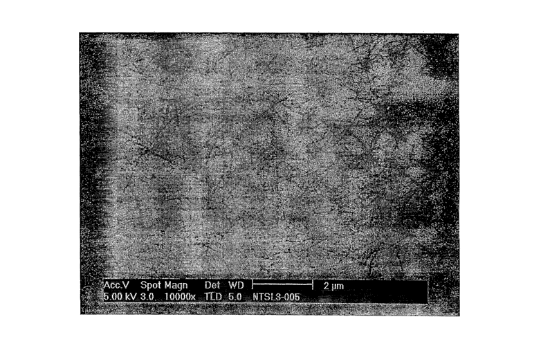
surface. Figures 1
and 3 illustrate SEM images of unpurified SWNT material and purified SWNT
material,
22
CA 02569349 2006-11-30
WO 2006/078293 PCT/US2005/017839
respectively coated from a solution of SWNTs in ethyl lactate. The presence of
particulate impurities is apparent in the unpurified sample (Fig. 1).
[0063] The purified SWNT film showed significant reduction in amorphous carbon
contamination after completion of the purification process (Fig. 2). The
figures do not
necessarily represent ideal electronics grade fabrics, but are shown simply to
represent
spun-on fabrics created from ethyl lactate.
[0064] Upon generation of a fabric the sheet resistance was measured to be 70
kOhm
(center); 129+l-22 kOhm (edge). The following table (Table 3) summarizes
several
metric parameters including the optical density of a typical purified SWNT
solution as
well as the resistivity of a SWNT fabric on a 100 mm silicon wafer coated with
a thick
gate oxide.
TABLE 3: Metrics of Typical SWNT Fabric
Metrics Data Remarks
O tical Density 1.001
(550 nm)
Sheet Resistance 70 kohm (center), 6 spins:
129+/-22 kohm (edge) 60 rpm, 500 rpm,
4000
rpm
[0065] The solution can be used to form a component of NRAM memories, such as
described in U.S. Patent Appl. No. 09/915093, entitled "Electromechanical
Memory
Array Using Nanotube Ribbons and Method for Making Same", filed July 25, 2001;
U.S.
Patent No. 6643165, entitled "Electromechanical Memory Having Cell Selection
Circuitry Constructed with Nanotube Technology," filed July 25, 2001; U.S.
Provisional
Patent Apl. No. 601459223, entitled "NRAM Bit Selectable Two-Drive Nanotube
Array,"
filed March 29, 2003; and U.S. Provisional Patent Appl. No. 60/459222,
entitled "NRAM
Byte/Block Released Bit Selectable One-Device Nanotube Array," filed March 29,
2003.
23
CA 02569349 2006-11-30
WO 2006/078293 PCT/US2005/017839
The solution holds potential as a stand alone commercial product to serve the
research
and development laboratories that work on single walled carbon nanotubes as
well other
applications.
EXAMPLE 5
[0066] This example describes the testing of trace metals on the surface of a
nanotube
article that is deposited on a silicon wafer.
[0067] A nanotube composition was prepared from nanotubes that had been
purified
of metallic and particulate impurities as described in Example 1 by dispersing
the
nanotubes in ethyl lactate medium as described in Example 2. The nanotube
compositions were analyzed for surface metallic impurities by Vapor Phase
Decomposition and Inductively-Coupled Plasma Mass Spectrometry (VPD, ICP/MS)
by
Chemtrace, Fremont, CA.
[0068] Silicon wafers, with and without a deposited nanotube layer, were
placed in a
pre-cleaned high purity chamber saturated with hydrofluoric acid (HF) vapor.
Untreated
silicon wafers and ethyl lactate coated wafers were used as controls. The
native or
thermal oxide on the silicon wafer or deposited layer was dissolved in the
presence of the
HF vapor. Metal impurities incorporated into the layer were released and
dissolved in the
acid during the scanning process.
[0069] A drop of an ultrapure acid etchant is added to the surface and the
analysis
area is scanned in a reproducible manner. The scanning solution was then
collected for
ICP-MS analysis. The analysis area was the entire surface on one side of the
wafer with 2
mm edge exclusion. Strict cleanroom practices were followed at all times. The
VPD
process was performed in a near Class 1 laminar flow mini-environment located
in a
Class 10 cleanroom. The ICP-MS instrument was operated in a Class 1000
cleanroom to
minimize environmental source contamination.
24
CA 02569349 2006-11-30
WO 2006/078293 PCT/US2005/017839
[0070] A pre-cleaned silicon wafer was used as the control. In order to
evaluate the
source of metallic impurities in the solvent, a silicon wafer was treated
(spin-coated) with
electronics grade ethyl lactate alone (EL Control). Samples 1 through 3
represent three
different nanotube compositions purified and prepared according to the
methodology set
out in Examples 1 and 2. The test results demonstrate that comparable levels
of purity
were achieved over a number of samples tested. Most of the metals tested were
near the
detection limit of the method. Notable exceptions to this were boron, calcium,
cobalt,
nickel potassium and sodium. However, the total and individual metals content
were well
below the lower limit of 15 x 101° atoms/cm3 set by the TTRS. Care must
be taken in post
purification processing in order to preserve the purity levels thus attained.
For example, it
was observed that rinsing the as-deposited nanotubes with DI water
reintroduced several
metal impurities.
[0071] The results of trace metal analysis recording the elemental content
SWNTs
after being coated on silicon substrates are reported in Table 4. Measurements
are
recorded as the number of atoms for a given element (X 101° atoms per
cm2).
CA 02569349 2006-11-30
WO 2006/078293 PCT/US2005/017839
TABLE 4 (Number Of Atoms For A Given Element X 101° Atoms Per
cm2).
Method
Detection Control EL Control Sample 1 Sample 2 Sample 3
Limits
Aluminum (AI) 0.3 0.91 0.57 0.78 0.33 <0.3
Antimony (Sb) 0.003 <0.003 <0.003 <0.003 <0.003 <0.003
Arsenic (As) 0.03 0.065 0.32 <0.03 <0.03 <0.03
Barium (Ba) 0.01 <0.01 <0.01 <0.01 <0.01 <0.01
Beryllium(Be) 0.1 <0.1 <0.1 <0.1 <0.1 <0.1
Bismuth (Bi) 0.002 <0.002 <0.002 <0.002 <0.002 <0.002
Boron (B 1 140 220 5.7 5.9 5.3
)
Cadmium (Cd) 0.005 <0.005 <0.005 <0.005 <0.005 <0.005
Calcium (Ca) 0.2 0.34 2.4 0.83 1.3 1.8
Chromium (Cr) 0.1 <0.1 0.11 <0.1 <0.1 <0.1
Cobalt (Go) 0.02 <0.02 <0.02 0.57 0.45 0.22
Copper (Cu) 0.05 <0.05 0.080 <0.05 0.34 <0.05
Gallium (Ga) 0.005 <0.005 <0.005 <0.005 <0.005 <0.005
Germanium(Ge) 0.01 <0.01 <0.01 <0.01 <0.01 <0.01
Iron (Fe) 0.1 <0.1 0.54 0.24 0.19 0.14
Lead (Pb) 0.003 <0.003 0.012 <0.003 0.011 <0.003
Lithium (Li) 0.08 <0.08 <0.08 <0.08 <0.08 <0.08
Magnesium(Mg) 0.3 <0.3 <0.3 <0.3 <0.3 <0.3
Manganese(Mn) 0.03 <0.03 0.069 <0.03 <0.03 <0.03
Molybdenum(Mo) 0.01 <0.01 0.014 <0.01 <0.01 <0.01
Nickel (Ni) 0.05 <0.05 <0.05 0.79 0.96 0.48
Potassium(K 0.2 <0.2 3.5 0.30 1.2 0.73
)
Sodium (Na) 0.2 <0.2 7.1 1.2 2.1 1.5
Strontium(Sr) 0.01 <0.01 <0.01 <0.01 <0.01 <0.01
Tin (Sn) 0.02 <0.02 <0.02 <0.02 <0.02 <0.02
Titanium (Ti) 0.1 <0.1 <0.1 <0.1 <0.1 <0.1
Tungsten (W 0.005 <0.005 <0.005 <0.005 <0.005 <0.005
)
Vanadium (V 0.03 <0.03 <0.03 <0.03 <0.03 <0.03
)
Zinc (Zn) 0.06 <0.06 1.4 0.088 0.095 0.078
Zirconium(Zr) 0.003 0.050 <0.003 <0.003 <0.003 <0.003
26
CA 02569349 2006-11-30
WO 2006/078293 PCT/US2005/017839
Other Embodiments
[0072] In certain embodiments concentrations of metallic or carbonaceous
contamination that are above those required for CMOS fabrication may be
acceptable.
The present invention serves to exemplify creation of nanotube solutions with
stringent
requirements that meet or exceed those of a CMOS process flow but can be
modified in
applications that have relaxed requirements.
[0073] In certain embodiments the SWNT solutions may be modified or tailored
to
form thick nanotube coatings up to 100 microns thick or more and as thin as a
monolayer
of SWNTs. Such nanotube fabrics can be characterized by resistivity or
capacitance
measurements to meet the requirements of the specific electronics application.
[0074] As described herein, certain applicator liquids and application
techniques are
described, which can be used to form nanotube films or fabrics of controlled
properties.
For example, certain proposals have been made suggesting the benefits of
substantially
monolayers of nanotubes with substantially uniform porosity. Techniques have
been
provided in which one or more parameters may be controlled or monitored to
create, such
films. Moreover, these liquids are intended for industrial environments, which
require
that the liquids be usable, i.e., that the nanotube suspension is stable, for
periods of days,
weeks and even months.
[0075] What is claimed is:
27