Note: Descriptions are shown in the official language in which they were submitted.
CA 02569586 2006-12-05
WO 2005/077021 PCT/US2005/003916
SYSTEMS AND METHODS FOR COMMUNICATING WITH
MULTIPLE DEVICES
CROSS REFERENCE TO RELATED APPLICATIONS
s This application is related to and claims priority from the United
States provisional patent application having application no. 60/542,742,
filed on February 6, 2004.
1. Field of the Invention
The invention relates in general to systems and methods for
communicating with multiple devices, and in particular to transferring data
between multiple devices in close proximity at high carrier frequencies.
2. Back rg ound
Recently, there has been a pronounced increase in the types of
communication applications that require the use of wireless data transfer.
15 Such applications include, for example, video conferencing, video-on-
demand, high speed Internet access, high speed local area networks, online
gaming, and high definition television. In the home or office, for example,
computing devices continue to be connected using wireless networking
systems. Many additional types of devices are also being designed with
2o wireless communication in mind. Moreover, there is a need to transfer data
at ever increasing rates.
There is also a need for a wireless device capable of high data rate
transfers which consumes less power. In particular, mobile computing
devices often have limited power supplies and require more efficient signal
2s propagation designs to maximize the use of such a device's power supply.
One way to increase the rate of data transfer is to use multiple transmit
and receive antennas while transmitting different data streams on these
different antenna simultaneously. However, this approach consumes more
power and requires more complex circuitry.
CA 02569586 2006-12-05
WO 2005/077021 PCT/US2005/003916
Thus, there exists a need for a system and method for transmitting
data at a high rate in an environment where potentially many devices in
close proximity are in communication with one another. Thus, what is
needed is an cost-effective technique that overcomes one or more of the
s aforementioned problems.
CA 02569586 2006-12-05
WO 2005/077021 PCT/US2005/003916
BRIEF SUMMARY OF THE INVENTION
Disclosed and claimed herein are systems and methods for
communicating with multiple devices. In one embodiment, a method
includes locating a plurality of wireless devices in proximity to each other,
where each the plurality of wireless devices operate at substantially the
same frequency. The method also includes transmitting a radio frequency
(RF) signal to one of the plurality of wireless devices along a line-of-sight,
and receiving the RF signal along the same line-of-sight. In one
embodiment, the RF signal is a substantially directional point-to-point
signal having a frequency on the order of 60 GHz.
Other aspects, features, and techniques of the invention will be
apparent to one skilled in the relevant art in view of the following detailed
description of the invention.
3
CA 02569586 2006-12-05
WO 2005/077021 PCT/US2005/003916
BRIEF DESCRIPTION OF DRAWINGS
FIG. 1A is a simplified diagram showing the signal spectrums for
multiple devices communicating in close proximity, according to one
embodiment of the invention;
FIG. 1B depicts the signal spectrum of convention transmitters;
FIG. 2 is a flow diagram illustrating one embodiment of a process for
transmitting signals, consistent with the principles of the invention;
FIGS. 3A-3b are simplified diagrams showing particular
embodiments of transmitter/receiver interactions, consistent with the
principles of the invention;
FIG. 4 is a schematic diagram for a receiving circuit, according to one
embodiment;
FIG. 5 is a schematic diagram for a switch of the receiving circuit of
FIG. 4, according to one embodiment;
15 FIG. 6 is a schematic diagram of another embodiment of the
receiving circuit of FIG. 4; and
FIG. 7 is a schematic diagram of yet another embodiment of the
receiving circuit of FIG. 4.
4
CA 02569586 2006-12-05
WO 2005/077021 PCT/US2005/003916
DETAILED DESCRIPTION OF THE PREFERRED EMBODIMENT
One aspect of the invention is to provide systems and methods which
transmit data wirelessly at a high data rate. In one embodiment, a
plurality of wireless devices in close proximity are able to transmit data at
a
high rate using a secure connection. While in one embodiment this data is
transmitted using a high speed, directional signal at a 60 GHz frequency, it
should be appreciated that the directional signal may be at a higher or
lower frequency.
In a further embodiment, data is transmitted at a high frequency
between a personal computing device and a plurality of consumer electronic
devices that are in relative close proximity to one another. The directional
nature of this high frequency signal permits a large number of devices in a
close proximity to communicate without interfering with each other.
Moreover, the directional nature of such a high frequency signal provides
~5 added communications security since the receiver will typically be in the
line of sight of the transmitter.
Another aspect of the invention is to use a direct current (DC)
detector to lower the required power consumption of an RF receiver. In one
embodiment, an RF receiver (or transceiver) is able to conserve power by
2o reducing or eliminating the need to continuously search for incoming
signals. This may be accomplished by a receiver operating in a first mode
and a second mode, according to one embodiment. In the first mode, the
receiver does not have to continuous search for and/or receiver a signal, but
rather may switch to the second mode upon detecting a DC voltage change
25 across one or more impedance elements, thereby indicating an incoming
signal. In another embodiment, or in the same embodiment, the first mode
is a "stand-by" mode which requires less power, and the second mode is an
"active" mode, during which the receiver is able to receive an RF signal. In
a further embodiment, the directional signal can be encoded with a
3o transmitter identification pattern recognizable only by the intended
CA 02569586 2006-12-05
WO 2005/077021 PCT/US2005/003916
receiver. Thus, the intended receiver may only switch to the second mode
when it detects a particular transmitter signal.
Referring to FIG. 1A, depicted one embodiment of a simplified
diagram of the paths of directional signals 110 of Transmitters A, B and C
while in communication with Receivers D, E and F. In one embodiment,
the signals are all RF signals transmitted at 60 GHz, while in another
embodiment the RF signals are transmitted at a frequency above 20 GHz.
For example, the RF signals may be transmitted at approximately 40 GHz,
122 GHz, 245 GHz, or at any other frequency at or above 20 GHz. It should
further be appreciated that the frequency to be used may depend on the
propagation loss and/or antenna structure used. With the directional
nature of signals 110, Transmitters A, B and C are able to communicate
with any combination of Receivers D, E and F without interference from
one another. In contrast, FIG. 1B depicts a simplified diagram of
conventional Transmitters D and E emitting lower frequency omni-
directional signals that overlap and hence interfere with one another.
In one embodiment, directional signals 110 may be achieved using
high frequencies, such as on the order of 60 GHz. In addition, spatially
orthogonal channels may be achieved with the use of high gain antennas
2o that are accurately aimed. Moreover, the shorter wavelength of higher
frequency signals allows smaller antennas to be used. Directional signals
reduce interferences, improve communication security, provide better QoS,
have a higher bit-rate per area and are more energy efficient.
FIG. 2 depicts one embodiment of how a plurality of wireless devices
2s in close proximity, such as the devices depicted in FIG. 1, may communicate
with each other in accordance with the principles of the invention. In
particular, process 200 begins at block 210 with the positioning and/or
orientation of the RF devices (e.g., transmitters, receiver and/or
transceivers) that are to communicate with each other. This device
so positioning and/or orientation should take into account the directional
nature of the high frequency signals to be transmitted by the RF devices.
6
CA 02569586 2006-12-05
WO 2005/077021 PCT/US2005/003916
Once the desired transmitters, receivers and/or transceivers have
been arranged properly, the high frequency signal may then be transmitted
at block 220. Assuming the devices were properly arranged, this directional
high frequency signal will be detected by its intended recipient device (e.g.,
s receiver, transceiver, etc.) at block 230. Once the transmission is
detected,
a series of device identification and compatibility "handshaking" may occur
at block 240. In one embodiment, this compatibility check may include
having a transmitter send out a high frequency signal containing a unique
pattern of on/off values. Upon receiving this unique pattern, a
corresponding receiver would then be able to consult a database to see if the
signal corresponds to a known transmitter. In another embodiment, after
receiving a known signal pattern (e.g., particular sequence of on/off values),
a receiver/transceiver may be return an acknowledgement signal to the
transmitting device. It should further be appreciated that the compatibility
check may also include the use of data encryption or similar data security
measures.
Thereafter, at block 250, a determination is made as to whether the
devices involved in the transmission in question are compatible. In one
embodiment, compatibility is determined by checking the frequency of the
2o incoming signal with the frequency at which the receiver operates. If the
devices are not compatible, the transmission fails and the process 200 will
end. If the devices are compatible, however, then process 200 continues to
block 260 where an authorization check is performed.
The authorization check of block 260 is optional depending on the
2s security needs of the given application. It should be appreciated that,
when
performed, the authorization check may be a simple authentication process
or may include more complex forms of authentication. In any event, if it is
determined at block 270 that the transmission is authorized, process 200
will continue to block 280 where the data transfer begins. If, on the other
3o hand, the transmission fails the authorization check, then the transmission
will fail and process 200 will end.
7
CA 02569586 2006-12-05
WO 2005/077021 PCT/US2005/003916
DC Detection
As mentioned above, another aspect of the invention is to use a direct
current (DC) detector, in combination with an RF receiver, to lower the
power consumption of the RF receiver. In one embodiment, an RF receiver
s (or transceiver) conserves power by operating in a "stand-by" mode, during
which the receiver circuitry does not have to continuously search for
incoming signals. Once a particular signal is detected by the DC detector,
however, the RF receiver can be made to switch to an "active" mode, after
which it may receive RF signals. This functionality may not be feasible to
implement with lower frequency systems since the signals would not be
directional and the receivers may have to be continuously operated to detect
incoming signals.
In FIG. 3A, Transmitter A from FIG. 1 is transmitting a high
frequency directional signal (e.g., higher than approximately 20 GHz).
15 However, since Receivers D and E are not oriented to be able to detect
signal 110 from Transmitter A, Receivers D and E remain in a stand-by
mode. As shown in FIG. 3B, the orientation of Transmitter A is shifted
such that signal 110 is detectable by Receiver D. When this signal is
detected by Receiver D, it can switch from a stand-by mode into an active
2o mode. Receiver E, still being out of range of signal 110, remains in stand-
by
mode thereby conserving power.
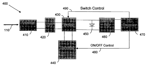
FIG. 4 is one embodiment of a receiving circuit 400 which utilizes DC
voltage detection to switch between a low power consumption mode and an
active mode. The up/down signal conversion operations of receiver 440
2s consume a relatively large amount of power. However, these operations
need only be performed while the receiver 440 is actively receiving and/or
searching for an RF signal. Thus, one aspect of the invention is to reduce
the amount of power the receiver 440 consumes by switching to a low power
consumption mode during which these up/down signal conversions will not
3o be performed. In one embodiment, the receiver 440 is turned off when it
enters the low power consumption mode. In one embodiment, the up/down
8
CA 02569586 2006-12-05
WO 2005/077021 PCT/US2005/003916
conversion is performed with a non-linear device (e.g., a diode, transistor,
etc.) and a local oscillator. Generation of a high frequency local oscillation
is not as efficient as a low frequency local oscillation. Thus, power
consumption can be reduced by reducing or removing the need to produce a
s high frequency local oscillation. Moreover, high speed communication
typically requires a wider bandwidth.
Continuing to refer to FIG. 4, receiving circuit 400 may receive RF
signal 110 using antenna 410. In one embodiment, the RF signal 110 is a
high frequency signal (e.g., higher than 20 GHz), while the antenna is a
directional antenna. The incoming signal 110 may pass through a low pass
filter (LPF) 420, which in one embodiment may alternately be integrated
with antenna 410.
The antenna 410 may have high pass filter (HPF) characteristics to
account for the high frequency signal to be received (e.g., 60 GHz).
~ s However, if the antenna 410 does not have HPF characteristics, then LPF
420 may be replaced with a band pass filter, according to one embodiment.
In another embodiment, or in addition to one or more of the previous
embodiments, a low noise amplifier (not shown) can be used with the
antenna 410.
2o As depicted in the embodiment of FIG. 4, switch circuit 430 is a
mufti-port circuit coupled to the antenna (via the LPF 420), a receiver 440
and a DC voltage detector 470. When the receiver 440 is in the low power
consumption mode, the switch circuit 430 may pass the incoming signal 110
on to the DC detector 470, as shown in FIG. 4, instead of passing it to the
2s receiver 440. However, before the signal is provided to the DC detector,
the
signal may be rectified using rectifying circuit 450 which, in one
embodiment is a diode-type circuit. However, it should be appreciated that
any rectifier may similarly be used. A second LPF 460 may also be used to
reduce signal harmonics effects prior to the DC detector 470.
3o If a valid signal is detected, which in one embodiment is a 60 GHz
signal, the DC detector 470 may emit switch control signal 490 to cause the
9
CA 02569586 2006-12-05
WO 2005/077021 PCT/US2005/003916
incoming signal 110 to pass to the receiver 440 rather than through to the
DC detector 480. Either before sending the switch control signal 490, or
simultaneously therewith, the DC detector 470 may provide an ON/OFF
control signal 480 to the receiver 440 to switch it from the low power
consumption mode into an active mode so that it can begin receive the
incoming signal 110. Thereafter, the switching circuit 430 will direct the
incoming signal 110 to the receiver 440.
FIG. 5 is a more detailed diagram of one embodiment of the
switching circuit 430 of FIG. 4. In this embodiment, incoming signal 110
enters the switch circuit 500 via transmission line (TL) 510. Depending on
the impendence along TL 520 and TL 550, after reaching Point A, the signal
110 may travel along either TL 520 or TL 550. In one embodiment, two-
state devices 540 and 570 are devices that can have two input impedance
states (e.g., matched and reflective, open and closed, etc.). Such devices
may include FETs, diodes, transistors, etc. When receiver 440 is in the low
power consumption mode, the impedance for device 570 may be set to 'open'
or 'reflective' using switch control signal 490. In this case, the signal 110
coming from Point A through TL 550 would be reflected back to Point A.
Moreover, by choosing an appropriate length L2 for TL 550, the impendence
20 looking from Point A into TL 550 would appear open. Similarly, using
switch control signal 490, device 540 can be set to matched (or closed),
allowing the signal 110 to move from Point A through TL 520 and through
to the rectifying circuit 450. In one embodiment, matching circuits 540 and
570 may be used to match the impedance between the transmission lines
2s (TL 520 and TL 550) and the two-state devices (devices 540 and 570). This
is due to the fact that, even when the two-state devices are matched, the
impedance of the two-state devices are not necessarily matched to the
transmission line impedance.
In contrast, when the receiver 440 is in the active mode, the
3o impedance for device 570 may be set to closed or matched. In this case, the
signal from Point A will flow through along TL 550, through device 570 and
CA 02569586 2006-12-05
WO 2005/077021 PCT/US2005/003916
into receiver 440. In one embodiment, device 570 is an FET and signal 110
is magnified before being passed to the receiver 440. In this case, the
impedance for device 540, on the other hand, may be set to reflective (or
open). Thus, by selecting the right length L1 for TL 520, the impedance
s looking from Point A into TL 520 can appear to be an open circuit, and the
incoming signal 110 will pass through TL 550 and into the receiver 440.
FIG. 6 depicts another embodiment of the receiving circuit 400 of
FIG. 4. In this embodiment, DC detector 470 is comprised of a reference
voltage source 610, comparator 620 and switch controller 630. In one
embodiment, comparator 620 compares the voltage from reference voltage
source 610 with the voltage passed by LPF 460. If the magnitude of the DC
voltage received from the LPF 460 is greater than the reference voltage, the
switch controller 630 may switch the output port of switching circuit 430
from the rectifying circuit 450 to the receiver 440. In one embodiment, this
15 1S done by using switch control signal 490. In another embodiment, the
switch controller 630 may also turn on receiver 440 using On/OFF control
signal 480. In yet another embodiment, the receiving circuit 400 may be a
transceiver. In such a case, the communication between the switching
circuit 430 and the receiver 440 will be bi-directional.
2o FIG. 7 is another embodiment of the receiving circuit 400 of FIG. 4 in
which the incoming signal is a 60 GHz signal and is encoded with an on/off
pattern 710. In this embodiment, the DC detection circuit 470 of receiving
circuit 700 includes reference voltage source 610, comparator 620, switch
controller 630 and on/off pattern detector 720. With such an arrangement,
2s a specific on/off pattern can be used to activate or "wake up" a receiver
which is in a low power consumption mode. Moreover, the on/off pattern
can be transmitter specific, thereby allowing the receiving circuit 700 to
remain in the low power consumption mode unless a predetermined
transmitter is detected. Thus, multiple receiving devices with the same
3o frequencies can be operated in close proximity without interfering with the
operation modes (e.g., stand-by, active, etc.) of each other.
11
CA 02569586 2006-12-05
WO 2005/077021 PCT/US2005/003916
While the preceding description has been directed to particular
embodiments, it is understood that those skilled in the art may conceive
modifications and/or variations to the specific embodiments described
herein. Any such modifications or variations which fall within the purview
of this description are intended to be included herein as well. It is
understood that the description herein is intended to be illustrative only
and is not intended to limit the scope of the invention.
12