Note: Descriptions are shown in the official language in which they were submitted.
CA 02569775 2006-12-06
WO 2005/122262 PCT/IB2005/051560
1
Method of manufacturing an image sensor and image sensor
The invention relates to a method of manufacturing a back-side illuminated
image sensor, comprising the steps of:
- starting with a wafer having a first and a second surface,
- providing light sensitive pixel regions extending into the layer of the
wafer
from the first surface,
- securing the wafer onto a protective substrate such that the first surface
faces
the protective substrate.
The invention further relates to an image sensor comprising a semiconducting
layer having a first and a second surface, the semiconductor layer comprising
liglit sensitive
regions extending into the semiconductor layer from the first surface, the
second surface of
the semiconductor layer having an optical transparant layer through which
light enters
through the semiconductor layer in the light sensitive pixel regions, the
first surface of the
semiconducting layer facing a protective substrate.
US 6,168,965 discloses a method for producing a back-illuminated image
sensor including a matrix of pixels (e.g. CMOS APS pixels) that are
manufactured on a
semiconductor substrate. The semiconductor substrate is secured to a
protective substrate by
an adhesive such that the processed frontside surface of the semiconductor
substrate faces the
protective substrate. With the protective substrate providing structural
support, the exposed
back-side surface of the semiconductor substrate is then subjected to grinding
and/or etching,
followed by optional chemical/mechanical processing, to thin the transparant
substrate to a
range of 10 to 15 microns. A transparant substrate (e.g. glass) is then
secured to the back-side
surface of the semiconductor substrate, thereby sandwiching the semiconductor
substrate
between the transparant substrate and the protective substrate.
Thinning of the transparant surface is a very non-uniform process in which
thickness variations of the semiconductor substrate results in differences in
absorption.
CA 02569775 2006-12-06
WO 2005/122262 PCT/IB2005/051560
2
The known image sensor therefore has the disadvantage that the efficiency is
limited and the variance in absorbtion of light is unacceptable high, in
particular for the short
wavelengths (blue).
It is an object of the invention to provide a method of manufacturing an image
sensor in which the efficiency is improved and the absorption variances are
reduced.
This object of the invention is achieved in that the wafer coinprises a
substrate
of a first material with an optical transparant layer and a layer of
semiconductor material,
wherein the substrate is selectively removed using the optical transparant
layer as stopping
layer.
The substrate can be selectively removed from the optical transparant layer by
using selective removal techniques towards the stopping layer. Such removal
techniques may
be wet chemical etching and/or chemical mechanical polishing (CMP). The
removal rate of
the stopping layer should be much less than the removal rate of the substrate
material. For
back-side illuminated image sensors, light has to transmit through the
semiconductor layer
and enter into the light sensitive pixel regions. It is therefore very
advantageous that the
semiconductor layer can be made relatively thin.
Because of the reduced thickness of the semiconductor layer, more light can
enter into the light sensitive regions, resulting in an improved efficiency of
the image sensor.
In particular short wavelenght light benefits from a reduced semiconductor
layer thickness.
Because the thickness and uniformity of the semiconductor layer can be very
well controlled, absorption differences between pixels and sensors are
significantly reduced.
Back-side illumination has many advantages compared to conventional image
sensors which are illuminated from the front-side. In conventional image
sensors the pixels
are driven by connection wires, which are usually manufactured from metal or
poly-silicon
layers. These layers are not transparant for light, so that incoming light can
not reach the
entire pixel area. There is a continious drive to reduce the pixel area to
reduce costs.
However, the further reduction of the pixel area in front-side illuminated
image sensors
inherently results in a relative smaller part of the pixel area being
sensitive to light.
In this invention where back-side illumination is applied, the poly or metal
connection wires no longer determine the light sensitive area of the pixel.
The entire pixel
area is sensitive to light, allowing a 100% fill factor. So advantages are,
amongst others, an
improved sensitivity, the angles of incoming light (CRA) can be larger and
there is more
CA 02569775 2006-12-06
WO 2005/122262 PCT/IB2005/051560
3
freedom in the design of the layout of connection wires. A larger chief ray
angle (CRA) can
result in a lower camera module because one lens element (e.g of a VGA lens in
a camera
module) may be omitted. This improves sensitivity (e.g. reduction of 2-4% in
reflection
losses) and reduces the costs. Also the building height of the module is lower
which is
important because of the miniaturization drive. Because of the trade-off
between the Module
Transfer Function (MTF) and the F-number, (MTF is a measure for the sharpness
and
contrast, and the F-number is a measure for the lens opening (diafragma)), the
extent to
which the MTF and F-number can be improved with back-side illumination is
exchangable.
It is advantageous when the optical transparant layer is a buried oxide layer
of
a silicon on insulator (SOI) wafer. The buried oxide of the SOI wafer can be
used as an etch
stop layer during removal of the silicon substrate. Nowadays, commercially
available SOI
wafers have an epitaxial semiconductor layer with a thickness of the order of
100 nm. After
removal of the substrate, the remaining epitaxial semiconductor layer still
has the initial
thickness and is very uniform. For amorphous and epitaxial semiconductor
layers, thickness
and uniformity can be controlled within a few nanometers.
It is another major advantage that the thin epitaxial semiconductor surface
remains protected by the buried oxide layer in the whole process. The surface
of the
semiconductor is not attached by processing, resulting in an almost perfect
silicon /oxide
interface without any defects, dangling bonds or interface charges.
With an SOI wafer is meant a silicon on insulator substrate. The silicon may
be strained. The invention works equally well for Ge on insulator (GeOI)
wafers, SiGe or any
compound thereof such as SiGeC on insulator wafers. It is advantageous to use
SOI wafers,
because these are commonly available, while other semiconductor on insulator
wafers are
still difficult to obtain and are very expensive.
Commercially available SOI wafers usually have an epitaxial semiconductor
layer with a thickness of the order of 100 nm. The absorption of light in the
light sensitive
regions in the semiconductor layer is optimal when the thickness of the
semiconductor layer
is less than 5 m, preferably in the range between 1-3 m. It is therefore
desirable to grow an
additional semiconductor layer epitaxially on the layer of semiconductor
material, to a total
thickness of the semiconductor layer of less than 5 microns.
Since the image sensor is back-side illuminated, a color filter may be
provided
on the optical transparant layer. The color layers may be spin coated and
developed after
exposure. The color fields (e.g. red, green and blue) of the (RGB) filter are
manufactured
CA 02569775 2006-12-06
WO 2005/122262 PCT/IB2005/051560
4
after each other. Light with a wavelength in the range of 400 and 700 nm is
filtered and each
wavelength passing the filter is collected in a different light sensitive
pixel region.
Apart from the advantages already mentioned, another advantage is the fact
that the efficiency of the sensor can be increased by using metal layers as
reflectors. A
special metallization pattern may be designed which functions as reflector to
re-direct light to
the light sensitive pixel regions. This is in particular of relevance when the
semiconductor
layer is much smaller than the total absorption depth of visible light. In
that case, light
entering from the back-side is reflected by the metallization pattern into the
light sensitive
pixel regions.
The different metal layers of the multilevel metallization can be used as
reflectors for different colors of light. In this way different colors are
reflected towards
different light sensitive pixel regions.
Special measures are taken to electrically isolate the light senstive area of
the
semiconductor epitaxial layer provided with the light sensitive pixel regions
from the rest of
the semiconductor epitaxial layer. To this end the metallization pattern
includes special
designed bond pad extensions for making outside contacts to the image sensor.
The outside contacts to the image sensor can be made either from the front
side or from the back-side. When the outside contacts are made from the back-
side via an
opening through the protective layer and the semiconductor layer to the bond
pad extensions,
. an advantage is that the semiconductor layer_is removed at the position of
the opening. The
opening in the semiconductor layer functions as an electrical separation
between different
dies. Another advantage of making electrical contact from the back-side (side
where the light
enters), is that the die can be connected easily to other substrates or ICs
e.g. by wire bonding
or flip-chip techniques. In the opening an electrical conductive stud can be
provided, which is
placed on the bond pad extensions. Such a stud may be advantageously be used
in a stud
bumping process.
When the outside contacts are made from the front-side, the advantage is that
there are no metal contacts hampering the light, which enters from the back-
side. In this case
special provisions should be made to obtain electrical isolation between
different dies. This is
described in the following embodiments.
Seen in perpendicular projection, a first part of the semiconductor layer
having
overlap with the bond pad extensions is electrically isolated from a second
part of the
semiconductor layer having the light sensitive pixel regions.
CA 02569775 2006-12-06
WO 2005/122262 PCT/IB2005/051560
The isolation between the first part and the second part of the semiconductor
layer can be formed by a trench extending through the entire semiconductor
layer. The trench
is filled with an electrical insulating material.
Alternatively the isolation between the first part and the second part of the
5 semiconductor layer can be formed by junction isolation.
In an alternative embodiment, the first part of the semiconductor layer below
the bond pads is removed, e.g. by etching.
In order to have a planar surface as long as possible in the manufacturing
process, the first part of the semiconductor epitaxial layer is removed late
in the process, after
the manufacture of the color filters. Because the color filters are made from
a photoresist,
these layers can also be used as an etch mask for etching the first part of
the semiconductor
layer below the bond pad extensions.
The color filter processing now can be done on a planar surface, which avoids
thickness variations and as a consequence fi-inging effects later in the
visible image of the
image sensor.
In another advantageous embodiment of the method the removal of the silicon
below the bond pad extensions can even be done after manufacturing of the
color filters and
the microlenses. After depositing the color filters and the microlenses, a
hard etch mask
layer, such as a plasma nitride layer, is deposited on the microlenses.
In this way "gapless microlenses" are formed..With this additional layer on
top
of the micro lenses, there is no spacing between these lenses so that the area
of the microlens
and the pixel area are the same.
The hard etch mask is used to etch the first part of the semiconductor layer
below the bond pads in order to electrical isolate the image sensing region
from the rest of
the semiconductor layer.
It is a further object of the invention to provide an image sensor in which
the
efficiency is improved and the absorption variances are reduced.
The object according to the invention is achieved in that part of the light
being
not absorbed in the semiconductor layer is re-directed into the light
sensitive pixel regions by
reflection of a metallization pattern. This is in particular of relevance when
the
semiconductor layer thickness is much smaller than the total absorption depth
of visible light.
In order to reduce losses, the metal layer facing the light sensitive regions
reflects the light
being not absorbed in the semiconductor layer and re-directs the light to the
light sensitive
pixel regions.
CA 02569775 2006-12-06
WO 2005/122262 PCT/IB2005/051560
6
Preferably, the metallization pattern is a multilevel metallization pattern,
and
different colors of light are reflected towards different light sensitive
pixel regions.
The efficiency of the sensor can be increased by using a multilevel
metallization in which the metal layers function as reflectors.
In an advantageous embodiment the image sensor comprises a metallization
pattern provided on the first surface of the semiconductor layer. The
metallization pattern
may comprise band pad extensions. An outside contact is arranged by connecting
the bond-
bad extensions via an opening through the semiconductor layer and the
protective layer from
the back-side (side where the light enters). An electrical contact from the
back-side is
advantageous because the die can be connected easily to other substrates or
ICs e.g. by wire
bonding or flip-chip techniques. In the opening an electrical conductive stud
or wire bond can
be provided, which is placed on the bond pad extensions. Such a stud may be
advantageously
be used in a stud bumping process.
How the present invention may be put into effect will now be described with
reference to the appended schematic drawings. Obviously, numerous variations
and
modifications can be made without departing from the spirit of the present
invention.
Therefore, it should be clearly understood that the embodiments of the present
invention are
illustrative only and not intended to limit the scope of the claims.
..
The features of the invention will be better understood by reference to the
accompanying drawings, which illustrate preferred embodiments of the invention
by way of
examples. In the drawings:
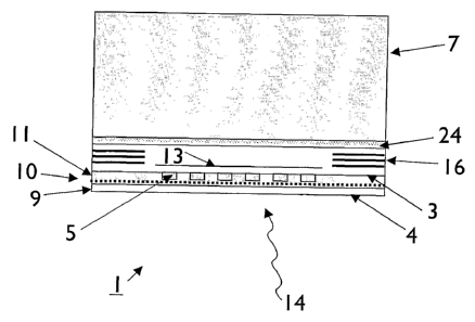
Fig. 1 shows a schematic representation of a CMOS image sensor according to
an embodiment of the invention. A protective substrate is glued to the first
side of the wafer.
Fig. 2 shows that the substrate is removed, using the buried oxide layer (BOX)
as etch stopping layer.
Figs. 3A and 3B show that the BOX oxide and the Si epi toplayer are etched at
the position of the bond pad extensions.
Fig. 4 shows that color filters and micro lenses are provided on the buried
oxide layer (BOX).
Fig. 5. shows that a second glass plate is glued on the color filters and
micro
lenses.
CA 02569775 2006-12-06
WO 2005/122262 PCT/IB2005/051560
7
Figs. 6 to 8 show that contacts from the bond pad extentions to the BGA balls
are made.
Figs. 7A-B to 8A show an alternative embodiment in which the bond pad
extensions are connected from the back-side.
Figs. 9 and 10 show in a second embodiment the removal of the silicon below
the bond pad extensions after manufacturing of the color filters.
Figs. 11 and 12 show the transmittance of two different color filters.
Figs. 13 to 16 show in a third embodiment the removal of the silicon below the
bond pad extensions after manufacturing of the color filters and microlenses.
Figs. 17 to 21 show in a fourth embodiment that the silicon below the bond
pad extensions is electrically isolated from the image sensing region by means
of an n-type
implantation in the semiconductor layer below the leads
Figs. 22 to 28 show in a fifth embodiment that the silicon below the bond pad
extensions is electrically isolated from the image sensing region by means of
deep trenches
filled with oxide arranged as a closed loop around the bond pad extensions.
Fig. 29 shows that the pixels are separated by the deep trenches.
Fig. 30 shows in a sixth embodiment two sensor pixels optimised for two
different wavelengths by choosing a different layer of metal. The use of
higher level metal
layers as reflectors cause different colors to be absorbed at different
locations.
The present invention will be described with respect to particular
embodiments and with reference to certain drawings but the invention is not
limited thereto
but only by the claims. The drawings described are only schematic and are non-
limiting. In
the drawings, the size of some of the elements may be exaggerated and not
drawn on scale
for illustrative purposes.
The terms top, bottom, over, under and the like in the description and the
claims are used for descriptive purposes and not necessarily for describing
relative positions.
It is to be understood that the terms so used are interchangeable under
appropriate
circumstances and that the embodiments of the invention described herein are
capable of
operation in other orientations than described or illustrated herein.
Starting material is a silicon on insulator (SOI) wafer 2 with a silicon
substrate
8 and a buried oxide 9 (BOX) thickness of 400 nm.
CA 02569775 2006-12-06
WO 2005/122262 PCT/IB2005/051560
8
The epitaxial semiconductor layer 10 is p-type with a typical doping
concentration of 1015 at/cm3 (resistivity of 10 Ohm.cm) and has a thickness of
100 nm.
Fig. 1 schematically shows the manufacture of the image sensor 1 on the SOI
wafer 2. In a first step, on top of the epitaxial semiconductor layer 10 of
the SOI wafer a
silicon layer 11 may be epitaxialy grown to a total thickness in the range of
1 to 3 microns.
To be used as an image sensor a two-dimensional array of photo-sensitive
elements 5 (diodes
or transistors) is manufactured in a CMOS process adapted to imaging. In the
metallization
traject special bond pad extensions 16 are manufactured to make contact
between the image
sensing region and the external bond pads later in the process. A protective
substrate 7 in the
form of a glass plate is secured with a layer of glue 24 on the first surface
3 of the wafer.
In Fig. 2 the substrate 8 of the SOI wafer is removed by grinding and a
subsequent etch in a solution of KOH. The etch rate of silicon in the KOH
solution is much
higher (typical 0.75 m /min ) than the etch rate of silicon oxide (typical 1
nm/min). A
selectivity of 100 can be easily obtained.
The buried oxide layer 9 functions as an etch stopping layer. The protective
substrate 7 facing the CMOS image sensors protects the semiconductor layer
from being
etched.
The silicon substrate 8 can also be removed by a wet etch in a solution of a
mixture of HF/HNO3 and subsequently in a solution of KOH.
In order to obtain electrical isolation between the semiconductor layer
comprising the photosenstive pixel regions (first part 20) and the rest of the
semiconductor
layer (second part 21), the second part 21 of the semiconductor layer is
removed.
To this end, in Fig. 3 the whole structure of Fig. 2 is turned upside down.
A resist mask 22 is provided on top of the image sensing part 20 in Fig. 3A.
The resist mask is used to etch the buried oxide 9 (BOX) and the Si epi top
layer 10 outside
the image sensing part 21, so above the bond pad extensions 16 (Fig. 3B).
Although not
shown in this Figure, the Si epi layer 10 is also removed above the leads
(forming contact
from bond pad extension to BGA balls) and above the bond pads. The resist mask
22 is
removed afterwards.
Alternatively, the buried oxide 9 can be etched using a resist mask and the
silicon epi layer 10 can be etched using an oxide hard mask.
In Fig. 4 the buried oxide 9 (BOX) is provided with color filters 12 and
microlenses (not shown in this Figure). The color filters and microlenses are
photo senitive
resist layers, which can be provided with photografic techniques. For the
alignment of the
CA 02569775 2006-12-06
WO 2005/122262 PCT/IB2005/051560
9
color fields 23 to the pixel 5 the same alignment marks can be used as in
standard CMOS
processes. These alignment marks are etched patterns in the silicon epi layer.
Because the
thickness of the epilayer is in the range of 1-3 m, the marks are easily
detectable by the
stepper. In order to expose the wafer from the back-side, special marks are
necessary, which
are mirrorred versions of the standard alignment marks.
In Fig. 5 a second glass plate 25 is secured on the color filter 12 and the
microlenses with a second glue layer 26.
In Fig. 6 a compliant layer 27 is provided.
In Fig. 7 the wafer is notched. The notch 28 ends in the upper glue layer 26.
In Fig. 8 metal leads 29 and a solder mask are provided. BGA balls 30 are
made.
The process shown in Figs. 6 to 8 is described in the wafer level package
process disclosed in W095/19645.
In an alternative embodiment shown in Figs. 7A-B to 8A the bond pad
extensions are connected from the back-side.
The second glass plate 25 (having a typical thickness of 400 m), is sawed
forming an opening 50 just above the bond pad extensions 16. The wafer
flatness and
tolerances in sawing make it very difficult to exactly stop on the metal
layers of the bond pad
extensions (see Fig. 7A). Therefore, the sawing process may be stopped when
there are only
- a few microns left between the opening 50 and the bond pad extensions 16
(see Fig. 7B).
Subsequently the remaining few microns of glass are removed. Preferably a
dry etching technique is used, using e.g. a fluorine containing gas. For wire
bonding,
preferably the bond pads closest to the semiconductor layer 10 are used. These
bond pads
closest to the semiconductor layer are formed from a thick metal layer which
is suitable for
wire bonding 51 (see Fig. 8A).
In the opening 50 a stud (e.g. of Cu) may be placed for stud bumping. Such a
stud may be placed on each level of the bond pads, because a stud can be
placed on a thin
metal layer. Preferably the stud protrudes the surface of the second glass
plate 25 for making
easily external contact in a stud bumping process such as flip chip.
In this alternative embodiment (Figs. 7A-B to 8A) an electrical connection is
provided from the back-side where the light enters. This is contrary to the
Figs.7 to 8 where
contact is made with solder balls from the other side. In mounting processes
for image
sensors, it is important that the wire bonding or stud bumping can occur from
the side where
the active area of the semiconductor is located. For example when die to die
bonding occurs
CA 02569775 2006-12-06
WO 2005/122262 PCT/IB2005/051560
with a companion die or when a bonding proces like I2MC is used. In several
modules a die
is mounted to the back-side of a flexible substrate with flip chip techniques.
In that case stud
bumps have to be provided at the same side where the active area of the
semiconductor is
located.
5 Already in the front-end of the CMOS process special measures have to be
taken for the separation of the image sensors later in the process.
The image sensors can be separated by first removing the semiconductor layer
surrounding the image sensors 21 in a method as described in US 6,177,295.
However this method is not suitable for the manuacture of CMOS image
10 sensors. For a good performance of the image sensor, the thickness of the
silicon toplayer 10
is in the range of 1-3 microns (instead of the 100 nm in US 6,177,295). If the
semiconductor
layer surrounding the image sensing devices is removed, a topography will
occur of 1-3
microns.
This topography may cause problems later in the process. It is not possible to
manufacture sub-micron devices in an advanced CMOS process on wafers with
several
microns topography.
In the method according to the invention, the silicon 21 below the bond pad
extensions is etched in a later stage of the process. A major advantage of
this shift towards
later processing, is that the advanced deep sub-micron CMOS process can be
done on a
planar surface of the wafer. I
Alternatively to the method as shown in Fig. 3A and 3B, in which the silicon
below the bond pad extensions is etched before the color filters are
manufactured, the
removal of the silicon 21 below the bond pad extensions 16 can be done after
manufacturing
of the color filters. The transparant resist layer 31 is used as a etch mask
for etching the oxide
layer 9 and subsequently the silicon epi layer 10.
Figs. 9 and 10 show this second embodiment of the method.
It is very advantageous that the color filter 12 processing now can be done on
a planar surface. The color fields 23 are manufactured by spin coating and
subsequent
development of the color layer. Different color fields 23 are manufactured
after each other
and are aligned above the pixels 5.
Figs. 11 and 12 show the color filter performance for visible light.
The transmission for blue, green and red are respectively about 80%, 80% and
more than 90%. This RGB filter is applied in mobile phones and webcams.
CA 02569775 2006-12-06
WO 2005/122262 PCT/IB2005/051560
11
The transmission for cyan, magenta and yellow are respectively about 80%,
90% and 95%. This CMY filter is applied in video applications.
Because the color filters are made from a photoresist, these layers can also
be
used as an etch mask for etching the silicon top layer below the bond pad
extensions. The
first layer of the color process is a transparant layer 31 which is exposed
and developed open
in an area of the bond pad extensions. The color layers and microlenses are
open exposed at
the position of the bond pad extensions, so that the BOX oxide 9 and the epi
layer 10 can be
etched using the color/microlenses sandwich as etch mask.
Figs. 13 to 16 show an advantageous third embodiment of the method in
which the removal of the silicon below the bond pad extensions can be done
after
manufacturing of the color filters and the microlenses 32.
This embodiment has the advantage of "gapless" microlenses. After depositing
the color filters 12 and the microlenses 32, a plasma nitride layer 33 is
deposited (see Fig.
13). In this way "gapless microlenses" are formed in Fig. 14. Lenses without
this extra layer
have a spacing between these lenses, so that the surface of the microlens is
smaller than the
pixel surface and part of the light can not enter. With this additional layer
33 on top of the
micro lenses 32, there is no spacing so that the area of the microlens and the
pixel area are the
same.
Subsequently a photoresist 34 is provided. The resist above the bond pad
extensions 16 is exposed and developed open. The plasma nitride 33, BOX oxide
9 and the
silicon epitaxial layer 10 are etched (see Fig. 15). The resist layer 34 on
top of the plasma
nitride layer may be selectively removed from the plasma nitride by stripping
in an oxygen
containing plasma (see Fig. 16). Alternatively this transparant resist can
remain there.
Compared to the second embodiment the advantages of the third embodiment
are:
- the color 12 layer and microlens layer 32 are protected against etching
steps by
means of the plasma nitride layer 33 and the resist layer 34.
- gapless microlenses 32 are obtained with a larger microlens area.
Instead of the nitride layer 33, as mentioned above, other materials such as
Al
can be used. An additional advantage of Al is that it can function as a light
shield.
In embodiments 4 and 5, the silicon 21 below the bond pad extensions 16 is
not removed, but electrically isolated from the image sensing region.
This may be realised by means of:
CA 02569775 2006-12-06
WO 2005/122262 PCT/IB2005/051560
12
- an n-type implantation 35 in the semiconductor layer below the leads
(embodiment 4) or
- trenches 40 filled with oxide arranged as a closed loop around bond pad
extensions (embodiment 5).
In embodiment 4, the semiconductor epi layer provided with the light senstive
pixel regions 20 is electrically isolated from the rest of semiconductor layer
21 where the
leads 29 will be positioned.
This electrical isolation is obtained by means of an N-type implantation. With
the aid of a resist mask, the epi top layer is implanted in an area 35 where
later in the process
contacts between the leads 29 and the bond pad extensions 16 will be made (See
Fig. 17, top
view). The N-type (P, As) implantation 37 is done at high energy (in the MeV
range) through
a resist mask 38. An oxide layer 39 protects the surface (Fig. 20). In order
to dope the entire
thickness of the epi layer a high temperature anneal is done after removal of
tlie resist layer
38 (see Fig. 21).
Later on in.the process, the metal leads 29 contact the N-type Si 35 and
therefore are electrically isolated from the P-type semiconductor layer 36
(see Fig. 18 cross
sectional view parallel to notch 28 line B-B', and Fig. 19 cross sectional
view perpendicular
to the notch 28, line A-A')
A big advantage of this method is that no fiuther topography is introduced on
the wafer.
In embodiment 5, the silicon layer where the leads make contact is
electrically
isolated from the semiconductor layer with the light sensitive pixel regions
by means of a
loop 40 around the bond pad extensions 16 (See Figs. 22,23,24). The loop is
formed by
etched trenches 41 which are filled with electrical isolating material like
silicon oxide (See
Figs. 25 to 28). After the trenches are filled with oxide, a planarisation
step is performed.
Alternatively the trenches may be filled with a thin (thermal) oxide and
polysilicon. The
polysilicon may be provided in a CVD process.
There are several methods of manufacturing the isolating loop. One of the
most elegant solutions is to combine this step with the manufacture of the
shallow trench
isolation step in conventional CMOS processing.
Just as is the case in STI processing, trenches are etched using an oxide 42
and
nitride hard 43 mask, they are filled with oxide 44 and planarised.
However, these STI trenches are not sufficiently deep to be applicable. A
subsequent trench etch has to be applied to etch the trench through the entire
thickness of the
CA 02569775 2006-12-06
WO 2005/122262 PCT/IB2005/051560
13
epi layer (3 to 5 microns). The buried oxide layer (BOX) functions as etch
stopping layer.
Figs 25 and 26 show respectively the etching of the shallow trench 46 and the
extra deep
trench 41. The filling with insulating material and the planarisation step can
be combined
with the standard STI process.
To this end a gapfill material 44 is deposited (Fig. 27). Preferably the width
of
the deep trench 41 is smaller than two times the thickness of the oxide 44 to
be deposited into
the trench in order to obtain a good planarisation. Subsequently the wafer is
planarised by
means of chemical mechanical polishing (CMP) (Fig. 28). Alternatively, the
trenches may be
filled with a thin (thermal) oxide and polysilicon. The polysilicon may be
provided in a CVD
process.
This embodiment 5 has the advantage of only one extra mask step and the
advantage that there is no further topography introduced in the process.
The pixels of the image sensing part can be separated from each other by
means of deep trenches 41. This is schematically shown in Fig. 29. Light
enters via a color
filter 23 into the light sensitive area of a pixel 5. The filtered light is
converted into'an
electrical current, generated in the depletion layer of the pn junction. The
depletion layer of
the pn junction may touch the surface of the interface between the BOX and the
epi-layer or
the sidewall of a deep trench.
It is also possible that the depletion layer is located in the bulk of the epi-
layer.
-The deep trenches for pixel isolation can be manufactured at the same time as
the deep trenches which are used for electrical isolation of the image sensing
part 20 from the
rest of the epi-layer 21.
In a further advantageous embodiment, the deep trenches are not filled with a
dielectric in this stage of the process. The trenches are filled in a next
step, in which the
planarisation layer (the transparant resist layer of embodiment 2) for the
color filter process is
provided. The advantage of this method is that the front-end processing is not
modified and
there are less resist variations in the color filter process.
An additional advantage of these deep trenches is that they can be used as
alignment marks. The marks are used to align the color filters and the micro
lenses above the
light sensitive pixel regions. Because the trenches extend through the entire
epi-layer, the
stepper may detect these trenches very well in this stage of the processs.
In back-side illuminated image sensors the light falls in from the back-side
14
of the semiconductor layer 10. Before entering into the depletion regions of
the junctions,
CA 02569775 2006-12-06
WO 2005/122262 PCT/IB2005/051560
14
which form the light sensitive pixel regions 5, light has to transmit through
the
semiconductor layer 10.
The absorption of visible light in the semiconductor layer, before entering
the
depletion region, can be reduced to zero. The depletion region of the
junctions touches the
transparant optical layer in that particular case.
When the semiconductor layer thickness is much smaller than the total
absorption depth of visible light, a certain amount of light will transmit
throught the
semiconductor layer.
This light may be reflected by a metallization pattern 13, which functions as
reflector.
To this end a special metallization pattern is designed in the CMOS
metallization traject.
The metallization pattern 13 is adapted to function as reflector to re-direct
light to the light sensitive pixel regions 5. In order to reduce losses, the
metal layer facing the
light sensitive -regions reflects the light being not absorbed in the
semiconductor layer and re-
directs the light to the light sensitive pixel regions.
The efficiency of the sensor can be increased by using a multilevel
metallization in which the metal layers function as reflectors. Fig. 30 shows
two sensor pixels
optimised for two different wavelengths by choosing a different layer of
metal.
The invention can be applied in CMOS imaging application areas, like
webcams and mobile phone cameras, PDAs (personal digital assistants) and DSCs
(digital
still cameras).