Note: Descriptions are shown in the official language in which they were submitted.
CA 02570172 2006-12-12
WO 2005/125063 PCT/US2005/020924
DESCRIPTION
FORWARD BASEBAND DIGITALIZATION
BACKGROUND INFORMATION
Field of the Invention
An embodiment of the invention relates generally to the field of data
networking.
More particularly, an embodiment of the invention relates to methods and
apparatus for
forward baseband digitalization.
Discussion of the Related Art
Prior art advanced broadband networks are known to those skilled in the art.
For
instance, a conventional advanced broadband network typically includes a
headend, a
number of hubs, and a larger number of nodes through which a still larger
number of
subscribers are serviced.
A problem with this technology has been related to the difficulty of achieving
highly
linear transmission over short and long fiber links at affordable cost. The
technology
commonly referred to as directly modulated 1310 nm analog lasers for 50 to 860
MHz
bandwidth is distance limited to 40 km and loss budget limited to 15-18 dB and
expensive at
high output levels that allow for such distant locations to be reached. The
technology
commonly referred to as externally modulated 1550 nm optical analog
transmitters for 50 to
860 MHz bandwidth is relatively very expensive for all distances and
practically not
applicable for distances in excess of 100 km. Therefore, what is required is
solution that
allows for much longer optical links at affordable cost and at the same or
better
performance.
Another problem with this technology has been that several links cascaded add
cumulatively interference levels. Therefore, what is also required is a
solution that allows for
cascading OEO signal regenerators without signal degradation.
One unsatisfactory approach to overcoming this distance limitations involves,
bandwidth splitting and using several separate transmitters to transmit much
lower
bandwidth, ideally within one frequency octave. However, a disadvantage of
this approach
is that it increases the cost of the link by the factor of two or higher.
Another unsatisfactory
approach for overcoming high loss budget with 1550 nm technology is to use
optical
amplification of the optical signal. However, a disadvantage of this approach
is significant
cost increase at low gains in loss budget and at measurable performance
degradation.
Therefore, what is also needed is a solution that meets the above-discussed
requirements in
a more cost-effective manner.
Heretofore, the requirements of long distance or high loss budget links at
affordable
-1-
CA 02570172 2006-12-12
WO 2005/125063 PCT/US2005/020924
cost without performance degradation, referred to above have not been fully
met. What is
needed is a solution that simultaneously meets all of these requirements.
SUMMARY OF THE INVENTION
There is a need for the following embodiments of the invention. Of course, the
invention is not limited to these embodiments.
According to an embodiment of the invention, a process comprises: receiving a
forward baseband digital optical signal from an optical fiber; transforming
the forward
baseband digital optical signal to a forward analog electrical signal;
transmitting the forward
analog electrical signal on an electrical conductor; receiving a reverse
analog electrical
signal on the electrical conductor; transforming the reverse analog electrical
signal to a
reverse digital baseband optical signal; and transmitting the reverse digital
baseband optical
signal. According to another embodiment of the invention, a machine comprises:
a forward
baseband digital optical signal receiver; a forward circuit coupled to the
forward baseband
digital optical signal receiver, the forward circuit transforming a forward
baseband digital
optical signal to a forward analog electrical signal; a forward analog
electrical signal
transmitter coupled to the forward circuit; a reverse analog electrical signal
receiver; a
reverse circuit coupled to the reverse analog electrical signal receiver, the
reverse circuit
transforming a reverse analog electrical signal to a reverse digital baseband
optical signal;
and a reverse baseband digital transmitter coupled to the reverse circuit.
These, and other, embodiments of the invention will be better appreciated and
understood when considered in conjunction with the following description and
the
accompanying drawings. It should be understood, however, that the following
description,
while indicating various embodiments of the invention and numerous specific
details thereof,
is given by way of illustration and not of limitation. Many substitutions,
modifications,
additions and/or rearrangements may be made within the scope of an embodiment
of the
invention without departing from the spirit thereof, and embodiments of the
invention include
all such substitutions, modifications, additions and/or rearrangements.
BRIEF DESCRIPTION OF THE DRAWINGS
The drawings accompanying and forming part of this specification are included
to
depict certain embodiments of the invention. A clearer conception of
embodiments of the
invention, and of the components combinable with, and operation of systems
provided with,
embodiments of the invention, will become more readily apparent by referring
to the
exemplary, and therefore nonlimiting, embodiments illustrated in the drawings,
wherein
identical reference numerals (if they occur in more than one view) designate
the same
elements. Embodiments of the invention may be better understood by reference
to one or
more of these drawings in combination with the description presented herein.
It should be
-2-
CA 02570172 2009-12-30
noted that the features illustrated in the drawings are not necessarily drawn
to scale.
FIG. 1 is a block schematic view of a network architecture with downstream
monitoring, representing an embodiment of the invention.
FIG. 2 is a block schematic view of a network architecture with a downstream
digital
transmission and downstream monitoring, representing an embodiment of the
invention.
DESCRIPTION OF PREFERRED EMBODIMENTS
Embodiments of the invention and the various features and advantageous details
thereof are explained more fully with reference to the nonlimiting embodiments
that are
illustrated in the accompanying drawings and detailed in the following
description.
Descriptions of well known starting materials, processing techniques,
components and
equipment are omitted so as not to unnecessarily obscure the embodiments of
the invention
in detail. It should be understood, however, that the detailed description and
the specific
examples, while indicating preferred embodiments of the invention, are given
by way of
illustration only and not by way of limitation. Various substitutions,
modifications, additions
and/or rearrangements within the spirit and/or scope of the underlying
inventive concept will
become apparent to those skilled in the art from this disclosure.
Within this application several publications are referenced by Arabic
numerals, or
principal author's name followed by year of publication, within parentheses or
brackets. Full
citations for these, and other, publications may be found at the end of the
specification
immediately preceding the claims after the section heading References.
The below-referenced U.S. Patents and U.S. Patent Applications disclose
embodiments that are useful for the purposes for which they are intended: U.S.
Pat. No(s).
6,452,708; 6,501,871; 6,618,522; 6,757,493; and 6,760,550; and Patent
Cooperation Treaty
Publication Nos. WO 01/052455; WO 02/021736; WO 02/021737; WO 02/091031; and
WO
03/081302.
In general, the context of an embodiment of the invention can include a data
network. The context of an embodiment of the invention can include a cable
television
network. The context of an embodiment of the invention can also include
Ethernet
networking.
-3-
CA 02570172 2006-12-12
WO 2005/125063 PCT/US2005/020924
The invention can include an optical network architecture for transporting
forward
analog signals in baseband digital form after analog to digital conversion and
converting
them to native analog signal at a location close to the customer, whether on
premises or in
the hybrid fiber coaxial and fiber networks. The invention can thereby provide
low
incremental cost digitized downstream distribution.
The invention can include baseband/wideband converting the forward analog
optical
signal to digital at a hub and converting the forward digital optical signal
to analog at a node,
optionally in the context of a hybrid fiber coax network. The
baseband/wideband conversion
can be defined as including a plurality of frequency octaves, preferably many
frequency
octaves. The invention can forward digitalize signals, for example, from
approximately 50
MHz to approximately 550 MHz or from approximately 50 MHz to approximately 870
MHz.
Thus, this aspect of the invention includes digital-to-analog forward
conversion at the node
(minifibernode). In one embodiment, the invention can include conveying from
approximately
to approximately 30 forward channels. In another, or the same, embodiment, the
15 invention can includes carrying reverse digital data up to approximately
100 MHz. Although
this extended reverse upper frequency range may involve more attenuation is
has the
significant advantage of less noise. It is important to note that the same
extended bandwidth
reverse chips found in some legacy nodes (minifibernodes) can provide the
digital-to-analog
downstream conversion. The baseband/wideband forward digitalization of the
invention
provides significant commercial advantages and is much more than just QAM
digitalization.
The invention can include the use of alternative sub-division schemes. The
invention
can include sub-dividing the forward throughput into multiple bandwidths (aka
chunks). In
one embodiment, the invention can sub-divide the forward throughput into one
or more
portion(s) that is(are) baseband digitized and one or more portion(s) that
is(are) analog. In
this fractional forward baseband digitalization embodiment, these portions are
subsequently
recombined at the node. For instance, an embodiment of the invention can
divide an input
from approximately 50 MHz to approximately 870 MHz into a first portion of
from
approximately 50 MHz to approximately 550 MHz for forward baseband
digitalization and a
second portion of from approximately 550 MHz to approximately 870 MHz for
analog.
The invention can include reducing the required forward digital bandwidth'by
a)
under sampling; b) space division multiplexing; and/or c) frequency down
conversion or
broadband conversion. For instance, given a forward signal domain of from
approximately 0
MHz to approximately 200 MHz, the invention can reduce the necessary sampling
frequency
from approximately 400 MHz to approximately 200 MHz by defining two sub-
sections
including a first sub-section of from approximately 0 MHz to approximately 100
MHz
corresponding to the domain of from approximately 0 MHz to approximately 100
MHz and a
-4-
CA 02570172 2006-12-12
WO 2005/125063 PCT/US2005/020924
second sub-section of from approximately 0 MHz to approximately 100 MHz
corresponding
to the domain of from approximately 100 MHz to approximately 200 MHz. This
embodiment
of the invention provides significant advantages with respect to expense, the
required speed
of the implementation circuitry and/or software, the required bandwidth to
implement the
embodiment, and the necessary sampling frequency, thereby yielding major
efficiency
improvements.
The invention can include subdividing the forward throughput into bandwidth
portions
that are equal to the reverse bandwidth of one or more minifibernodes (that
may already be
deployed). For instance, an embodiment of the invention can subdivide the
forward
throughput into multiple portions of from approximately 0 MHz to approximately
42 MHz, or
from approximately 0 MHz to approximately 45 MHz, or from approximately 0 MHz
to
approximately 96 MHz, or from approximately 0 MHz to approximately 100 MHz.
This
embodiment of the invention is very efficient with regard to utilizing
existing legacy
equipment (e.g., previously deployed minifibernodes) and is, therefore, a
commercially
important aspect of the invention.
The invention can optionally include providing Ethernet in the forward
direction via
the forward digitized signals. The invention can include alternative ways to
allocate the
Ethernet data at the hub and alternative ways to recover it at the node.
Referring to FIG. 1, a downstream transmitter block 1000 is coupled to a
digital
return transceiver block 1065. The digital return transceiver block 1065 is
coupled to a digital
return receiver block 1155.
Still referring to FIG. 1, a processing block 1010 is coupled to a serializer
block 1020.
A monitoring block uC 1030 is also coupled to the processing block 1010. The
serializer
block 1020 is coupled to an optical transmitter block 1040. The optical
transmitter block
1040 is coupled to fan-out (e.g., splitter, router, etc.) block 1050. The fan-
out block 1050 is
coupled to an optical link 1055. The optical link 1055 is coupled to an
optical receiver block
1060. The optical receiver block 1060 is coupled to a deserializer block 1070.
The
deserializer block 1070 is coupled to a processing block 1080. An upstream
data signal is
provided to a low pass filter 1090. The low pass filter 1090 is coupled to an
analog-to-digital
converter 1100. A clock 1110 is also coupled to the analog-to-digital
converter 1100. The
analog-to-digital converter 1100 is coupled to the processing block 1080. A
monitoring block
uC 1120 is also coupled to the processing block 1080. The processing block
1080 is
coupled to a serializer block 1130. The serializer block 1130 is coupled to an
optical
transmitter block 1140. The optical transmitter 1140 is coupled to an optical
link 1145. The
optical link 1145 is coupled to an optical receiver block 1150. The optical
receiver block
1150 is coupled to a deserializer block 1160. The deserializer block 1160 is
coupled to a
-5-
CA 02570172 2006-12-12
WO 2005/125063 PCT/US2005/020924
processing block 1170. A monitoring block uC 1180 is also coupled to the
processing block
1170. The processing block 1170 is coupled to a digital-to-analog converter
1190. A clock
1200 is also coupled to the digital-to-analog converter 1190. The digital-to
analog converter
1190 is coupled to a low pass filter 1210, thereby providing a regenerated
upstream signal.
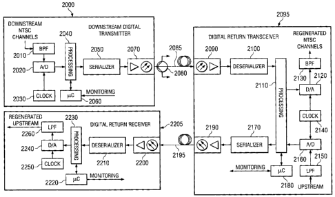
Referring to FIG. 2, a downstream digital transmitter 2000 is coupled to a
digital
return transceiver 2095. The digital return transceiver 2095 is coupled to a
digital return
receiver 2205.
Still referring to FIG. 2, a downstream data signal including NTSC (National
Television System Committee) channels is provided to a band pass filter 2010.
The band
pass filter 2010 is coupled to an analog-to-digital converter 2020. A clock
2030 is also
coupled to the analog-to-digital converter 2020. The analog-to-digital
converter 2020 is
coupled to a processing block 2040. The processing block 2040 is coupled to a
serializer
block 2050. A monitoring block uC 2060 is also coupled to the processing block
2040. The
serializer block 2050 is coupled to an optical transmitter block 2070. The
optical transmitter
block 2070 is coupled to fan-out (e.g., splitter, router, etc.) block 2080.
The fan-out block
2080 is coupled to an optical link 2085. The optical link 2085 is coupled to
an optical
receiver block 2090. The optical receiver block 2090 is coupled to a
deserializer block 2100.
The deserializer block 2100 is coupled to a processing block 2110. The
processing block is
coupled to a digital-to-analog converter 2120. The digital-to-analog converter
2120 is
coupled to a band pass filter 2130, thereby providing regenerated NTSC
channels. The
digital-to-analog converter 2120 is also coupled to a clock 2140. An upstream
data signal is
provided to a low pass filter 2150. The low pass filter 2150 is coupled to an
analog-to-digital
converter 2160. The clock 2140 is also coupled to the analog-to-digital
converter 2160. The
analog-to-digital converter 2160 is coupled to the processing block 2110. A
monitoring block
uC 2180 is also coupled to the processing block 2110. The processing block
2110 is
coupled to a serializer block 2170. The serializer block 2170 is coupled to an
optical
transmitter block 2190. The optical transmitter 2190 is coupled to an optical
link 2195. The
optical link 2195 is coupled to an optical receiver block 2200. The optical
receiver block
2200 is coupled to a deserializer block 2210. The deserializer block 2210 is
coupled to a
processing block 2230. A monitoring block uC 2220 is also coupled to the
processing block-
2230. The processing block 2230 is coupled to a digital-to-analog converter
2240. A clock
2250 is also coupled to the digital-to-analog converter 2240. The digital-to
analog converter
2240 is coupled to a low pass filter 2260, thereby providing a regenerated
upstream signal.
An embodiment of the invention can also be included in a kit. The kit can
include
some, or all, of the components that an embodiment of the invention includes.
The kit can
be an in-the-field retrofit kit to improve existing systems that are capable
of incorporating an
-6-
CA 02570172 2006-12-12
WO 2005/125063 PCT/US2005/020924
embodiment of the invention. The kit can include software, firmware and/or
hardware for
carrying out an embodiment of the invention. The kit can also contain
instructions for
practicing an embodiment of the invention. Unless otherwise specified, the
components,
software, firmware, hardware and/or instructions of the kit can be the same as
those used in
an embodiment of the invention.
Embodiments of the invention, can be cost effective and advantageous for at
least
the following reasons. The invention enables longer range communications. The
invention
justifies accounting the capital costs of the components to more subscribers.
The invention
avoids loss of fidelity. The invention permits targeting data to particular
subscribers.
Embodiments of the invention improves quality and/or reduces costs compared to
previous
approaches.
The term plurality is defined as two or more than two. The term another is
defined as
at least a second or more. The terms "consisting" (consists, consisted) and/or
"composing"
(composes, composed) are defined as close language that does not leave the
recited
method, apparatus or composition to the inclusion of procedures, structure(s)
and/or
ingredient(s) other than those recited except for ancillaries, adjuncts and/or
impurities
ordinarily associated therewith. The recital of the term "essentially" along
with the terms
"consisting" (consists, consisted) and/or "composing" (composes, composed), is
defined as
modified close language that leaves the recited method, apparatus and/or
composition open
only for the inclusion of unspecified procedure(s), structure(s) and/or
ingredient(s) which do
not materially affect the basic novel characteristics of the recited method,
apparatus and/or
composition. The term coupled is defined as connected, although not
necessarily directly,
and not necessarily mechanically. The term proximate, as used herein, is
defined as close,
near adjacent and/or coincident; and includes spatial situations where the
specified
functions and/or results can be carried out and/or achieved. The phrase radio
frequency, as
used herein, is defined as including infrared, as well as frequencies less
than or equal to
approximately 300 GHz.
The term any is defined as all applicable members of a set or at least a
subset of all
applicable members of the set. The term approximately is defined as at least
close to a
given value (e.g., within 10% of). The term substantially is defined as
largely but not
necessarily wholly that which is specified. The term generally is defined as
at least
approaching a given state. The term deploying is defined as designing,
building, shipping,
installing and/or operating. The term means, when followed by the term "for"
as used herein,
is defined as hardware, firmware and/or software for achieving a result. The
terms program
or computer program are defined as a sequence of instructions designed for
execution on a
computer system (e.g., a program, or computer program, may include a
subroutine, a
-7-
CA 02570172 2006-12-12
WO 2005/125063 PCT/US2005/020924
function, a procedure, an object method, an object implementation, an
executable
application, an applet, a servlet, a source code, an object code, a shared
library/dynamic
load library and/or other sequence of instructions designed for execution on a
computer or
computer system).
As used herein, the terms "comprises," "comprising," "includes," "including,"
"has,"
"having" or any other variation thereof, are intended to cover a non-exclusive
inclusion. For
example, a process, method, article, or apparatus that comprises a list of
elements is not
necessarily limited to only those elements but may include other elements not
expressly
listed or inherent to such process, method, article, or apparatus. Further,
unless expressly
stated to the contrary, "or" refers to an inclusive or and not to an exclusive
or. For example,
a condition A or B is satisfied by any one of the following: A is true (or
present) and B is
false (or not present), A is false (or not present) and B is true (or
present), and both A and B
are true (or present).
Also, use of the "a" or "an" are employed to describe elements and components
of
the invention. This is done merely for convenience and to give a general sense
of the
invention. This description should be read to include one or at least one and
the singular
also includes the plural unless it is obvious that it is meant otherwise.
Unless otherwise defined, all technical and scientific terms used herein have
the
same meaning as commonly understood by one of ordinary skill in the art to
which this
invention belongs. In case of conflict, the present specification, including
definitions, will
control. In addition, the materials, methods, and examples are illustrative
only and not
intended to be limiting.
All the disclosed embodiments of the invention disclosed herein can be made
and
used without undue experimentation in light of the disclosure. An embodiment
of the
invention is not limited by theoretical statements recited herein. Although
the best mode of
carrying out embodiments of the invention contemplated by the inventor(s) is
disclosed,
practice of an embodiment of the invention is not limited thereto.
Accordingly, it will be
appreciated by those skilled in the art that an embodiment of the invention
may be practiced
otherwise than as specifically described herein.
It will be manifest that various substitutions, modifications, additions
and/or
rearrangements of the features of an embodiment of the invention may be made
without
deviating from the spirit and/or scope of the underlying inventive concept. It
is deemed that
the spirit and/or scope of the underlying inventive concept as defined by the
appended
claims and their equivalents cover all such substitutions, modifications,
additions and/or
rearrangements.
All the disclosed elements and features of each disclosed embodiment can be
-8-
CA 02570172 2006-12-12
WO 2005/125063 PCT/US2005/020924
combined with, or substituted for, the disclosed elements and features of
every other
disclosed embodiment except where such elements or features are mutually
exclusive.
The appended claims are not to be interpreted as including means-plus-function
limitations, unless such a limitation is explicitly recited in a given claim
using the phrase(s)
"means for" and/or "step for." Subgeneric embodiments of the invention are
delineated by
the appended independent claims and their equivalents. Specific embodiments of
the
invention are differentiated by the appended dependent claims and their
equivalents.
-9-