Note: Descriptions are shown in the official language in which they were submitted.
CA 02570189 2006-12-13
WO 2006/004957 PCT/US2005/023377
Title
SUB-MICRON SOLID OXIDE ELECTROLYTE MEMBRANE
Field
The invention relates to electrolyte membranes, and, more particularly, to
thin film
solid oxide electrolyte membranes.
Background
Fuel cells have great potential for supplying inexpensive and clean electrical
power.
One common type of fuel cell is the hydrogen fuel cell. The basic operation of
the hydrogen
fuel cell includes the migration of hydrogen ions through a semi-permeable
membrane
known as an electrolyte membrane (or layer). Another type of fuel cell is the
solid oxide fuel
cell (SOFC). The SOFC worlcs in part by migrating oxygen ions through the
electrolyte
layer. For any fuel cell, the ideal electrolyte layer will transport only the
desired type of ion.
A fuel cell is an electrochemical device that produces electrical current from
chemical
reaction. The fundamental device includes an ion-conducting electrolyte
between two
electrodes, backed by fuel and oxidant flow distributors. At the oxidant side
a catalyst on the
electrode promotes combination of ions and electrons. At the fuel side a
catalyst on the
electrode promotes separation of ions and electrons. Only the ions conduct
through the
electrolyte while the electrons are conducted through an external circuit,
thus supplying
electrical power. SOFC's have oxygen ion-conducting metal oxide membranes as
their
electrolyte layer. The oxygen molecules transform into oxygen ions by
receiving electrons
from electrode/catalyst at the oxidant side. The oxygen ions propagate through
the
electrolyte membrane and combine with hydrogen molecules into water by leaving
electrons
to electrode/catalyst at the fuel side. A gas sensor has same basic
configuration, and
produces electrical current that depends on difference of gas concentration.
Fuel cell operation is increasingly efficient when the electronic conductivity
of the
electrolyte is minimized and the ionic conductivity of the electrolyte is
maximized. It is well
lcnown that a fuel cell is thermodynamically more efficient at lower
temperatures, with lower
entropic losses resulting in a higher open cell voltage.
SOFC's have a several of advantages compared to hydrogen fuel cells including:
no
humidity requirement for ion exchange, no water clogging up with generated
water, no or
less noble metal catalyst, high CO tolerance, and useable waste heat.
1
CA 02570189 2006-12-13
WO 2006/004957 PCT/US2005/023377
However, conventional SOFC's also have problems. One of the main problems to
be
overcome is preparation of hermetic seals at high temperatures. With operating
temperatures
decreasing from 1000 C to 700 C or less, metal materials can be used for
sealing and the
sealing problem becomes manageable. Many efforts have been made to decrease
the
operating temperature of SOFC's to below 700 C despite a large loss of output
power.
However, these operating temperatures are still too high for mobile
applications.
Fig. 1 shows a prior art electrolyte and porous electrode combination. The
porous
nature of the electrode 104 means that the thickness of the electrolyte 102 is
quite large. The
porous electrode 104 allows gases to reach the electrolyte 102. The
electrolyte 102 should
have sufficient thickness such that there are no gaps in the electrolyte 102
as the electrolyte
102 is deposited on the electrode 104. The resulting thick electrolyte 102
layer leads to high
resistance.
Figs. 2A-B show a prior art electrolyte and dense electrode combination. This
combination can be seen in US Patent No. 6,645,656. A dense electrode 204
contacts an
electrolyte 102 layer. The electrode 204 is etched, as seen in Fig. 2B, to
allow gases to reach
the electrolyte 102.
SOFC's have adopted stabilized zirconia for oxygen ion conducting electrolyte
layers
for several decades. Due to the low ionic conductivity at low temperature,
such SOFC's have
to be operated above 800 C. High operation temperature limits the choice of
materials for
stacking and sealing and brings in numerous problems (corrosion and
degradation for
example). These problems have so far resulted in high costs and limited
applications, even
though SOFC's have many advantages over the other power systems (environment
protection
for example). Therefore, lowering the operating temperature of a SOFC in a
stationary
power system is desirable. Other potential applications, including electric
vehicles and
portable electronics, are another driving force to lower the operating
temperature of SOFC.
One way to achieve lower operating temperatures is by choosing ceramic
electrolytes with
higher oxygen ion conductivities at lower temperature. Another way is by
reducing the
thiclcness of the electrolyte membrane.
Doped ceria is one of the suitable electrolyte candidates for low-temperature
SOFC.
One common dopant is Gd203 and typical composition for Gd-doped Ceria is
Gdo.2Ceo.s01.9-
x
(GDC). Oxygen ion conductivity in doped ceria is understood to be two to three
orders
higher than that of yttria stabilized zirconia (YSZ) at low temperatures.
Doped ceria has not
been successfully used in a SOFC because it will transfer into a mixed
conductor under
2
CA 02570189 2006-12-13
WO 2006/004957 PCT/US2005/023377
reduced atmosphere and as a result short-circuit the cell at around 700 C.
Fortunately, the
ionic domain of doped ceria increases as the temperature decreases. At a
temperature of 500
C, with a favorable SOFC anodic condition, the ionic transference number of
doped ceria is
larger than 0.9. Therefore, doped ceria is one of the suitable candidates for
low temperature
SOFC.
Thus, there is a need for a solid oxide electrolyte membrane with high ionic
conductivity and physical properties that allow solid-state ionic devices to
be able to operate
at low temperatures.
Summary
This document describes thin film solid oxide electrolyte membranes.
Brief Description of the Drawings
Fig. 1 shows a prior art electrolyte and porous electrode combination.
Figs. 2A-B show a prior art electrolyte and dense electrode combination.
Fig. 3 shows an exemplary electrolyte and dense electrode combination.
Fig. 4 shows an exemplary fuel cell.
Figs. 5A-M show an example of a method of making a fuel cell on a dense
substrate.
Fig. 6 shows an example of a porous platinum electrode.
Fig. 7 shows an example of fuel cell with Pt and YSZ.
Figs. 8A-B show examples of how fuel cells may be grouped on a wafer.
Fig. 9 shows examples of grain boundaries in an electrolyte.
Fig. 10 shows examples of grain boundaries in an electrolyte.
Fig. 11 shows exemplary isothermal curves for area specific resistances of
10[tm and 100nm
thick yttira stabilized zirconia and gadolinia doped ceria.
Fig. 12 shows isothermal curves for ionic conductivities of gadolinia doped
ceria with
various thicknesses.
Fig. 13 shows an example of calculated fuel cell perfozmance vs. experimental
data.
Figs. 14A-C show examples of ion highways.
Fig. 15 shows an exeinplary dense Pt electrode, GDC electrolyte, and dense Pt
electrode
combination for electrochemical characterization.
Description
The present invention provides nano-scale thin solid oxide electrolyte
membranes,
3
CA 02570189 2006-12-13
WO 2006/004957 PCT/US2005/023377
which can significantly reduce ionic resistance loss from the electrolyte as
well as catalytic
loss from charge transfer reaction that occurs at gas/electrode/electrolyte
triple phase
boundaries. One preferred embodiment is based on:
1. Conventional ion conducting materials, such as, but not limited to
stabilized
zirconia or doped ceria, as solid electrolyte membranes.
2. Decreasing area specific resistance from the electrolyte as a result of the
decrease of the thickness and/ or increase of the ionic conductivity.
3. Increase of the ionic conductivity due to one or more of the following
reasons: elimination of cross grain boundaries, self-generated ion
highways resulting from segregation of dopants or space charge
overlapping, artificially generated ion highways like irradiation-induced
dislocations.
4. Increase of the charge transfer reaction rate as a results of special
surface
charge and/or electric field distribution.
Some of the advantages of the present invention over existing devices and
methods
include:
1. High power density/efficiency fuel cells and highly sensitive gas sensors
at
lower operating temperatures due to the low area specific resistance from
electrolyte and high charge transfer reaction rate.
2. Solving high temperature operation problems caused by difference of
thermal expansion coefficient between electrode and electrolyte materials,
and also enabling free device design by enlarged availability of materials
including inetals and polymers.
For practical application the resistance per cm2, the so called area specific
resistance
(ASR), from the electrolyte is desirably less than 0.1 ohm per cm2. Since ASR
changes
proportionally to the thickness of the electrolyte, with an inverse
relationship with ionic
conductance, it is beneficial to use a thin film electrolyte in a SOFC for
lower operating
temperatures. The ASRs of YSZ and GDC were calculated assuming 10 m and 100
nm
thiclcness in the temperature range of 100 C to 1000 C. The 10 m thick
electrolyte is
mostly applied in either laboratory or pilot-line SOFC systems. The minimum
operating
temperature by using 10 m YSZ and GDC as an electrolyte will be 700 C and
500 C
respectively. As the thiclcness of YSZ and GDC electrolyte is reduced to 100
nm, the
4
CA 02570189 2006-12-13
WO 2006/004957 PCT/US2005/023377
operating temperature of SOFC can be decreased down to 400 C to 200 C by
neglecting the
liinitations from the electrode reaction.
There have been many recent studies on sintered electrode supported thin film
SOFC's. The typical electrolyte thiclcness found in most of these studies is
around 5-20 m,
with operating temperatures in the range of 500 - 1000 C. Although sintered-
fabricated
electrodes offer a porous morphology for gas diffusion, it is difficult to
deposit a thin, pinhole
free electrolyte layer onto these electrodes, because the pore sizes are
usually larger than the
thickness of the electrolyte. In addition, the sintering method is not
compatible with
semiconductor fabrication techniques. In contrast, sputtering methods are
widely used in
semiconductor process flows and can yield a range of film morphologies (i.e.
dense or porous
films) by adjusting deposition parameters, such as gas pressure, deposition
power and
deposition temperature. We find that the ability to fabricate sputtered,
nanoporous electrodes
to be a desirable enabling feature of our design. These nanoporous electrode
structures grant
process compatibility with our other fabrication steps while also offering the
possibility to
successfully support a thinner electrolyte.
Theoretically, reducing electrolyte thickness should result in better SOFC
performance at a given temperature. However, electrolyte scaling presents
several major
challenges, such as ensuring the mechanical stability of the structure,
maintaining the
electrical conductivity of the electrodes, avoiding electrical short circuit
problems in the
electrolyte, and ensuring gas tightness in the electrolyte layer.
In an effort to reduce electrolyte thiclcness, several groups have adopted Si-
based thin
film SOFC's. The thickness of electrolyte in these devices is around 1.2 m.
These studies
have used sputtering and photolithographic techniques in their fabrication.
We have targeted even thinner electrolyte layers. The stacking structure of an
exemplary thin-film SOFC comprises a 150 nm thick YSZ electrolyte layer
sandwiched in-
between two layers of 200 nm thick porous Pt electrode. DC- and RF-magnetron
sputtering
may be used for the deposition of nanoporous Pt and dense YSZ layers
respectively.
Standard photolithographic techniques may be used to fabricate the layered
structure.
For dense substrates, a relative density greater than 80% is preferable. A
relative
density greater than 90% may be more preferable. A relative density greater
than 95% may
be even more preferable. The densities are relative to the maximum theoretical
material
density. If porosity is zero, then relative density is 100%.
A thin smooth YSZ layer may be fabricated between non-smooth nanoporous Pt
layers by using a novel fabrication process. YSZ may be deposited on a smooth
SiN layer.
5
CA 02570189 2006-12-13
WO 2006/004957 PCT/US2005/023377
Pt may be deposited onto the YSZ layer after etching of the SiN. Porous Pt
films may be
achieved by varying the sputtering conditions (i.e. high Ar pressure and low
DC power).
Because of the fragile nature of the thin-film structure, a difficult
compromise
between size and mechanical stability may be made. Employing larger device
areas allows
greater current/power production, but sacrifices mechanical strength. To
ensure the
mechanical stability of the membrane, one may use small cell sizes of about 50
m x 50 m
to 400 m x 400 m. Thus, the effective small fuel cell surface area may range
from 2.5 x
10-9 to 1.6 x 10⁻⁷ m2. Examples of side length dimensions for square profiled
small fuel cells
include 50, 75, 100, 150, 190, 245, 290, 330, 370, 375, and 400 m. While each
individual
cell may be extremely small, more than 1500 cells can be realized on a 4-inch
silicon wafer.
In order to ascertain the optimal compromise between cell size, power density,
and
mechanical stability, the shape and size of the windows on the silicon wafer
as well as the
processing methods may be examined in detail. As further characterization, the
impedance of
the thin film YSZ, as well as OCV and current/voltage curves of the Si-based
SOFC's may be
measured.
The wafer may be a 4-inch diameter and 375 m thick (100) silicon wafer with
500
nm of low stress silicon nitride deposited on both sides by Low Pressure CVD
(LPCVD).
SPR3612 photo resist may be coated on the backside, then exposed and developed
by a photo
resist spin coater (SVG coater), a optical aligner (EV aligner) and a
developer (SVG
developer) respectively. Then, the silicon nitride may be etched away in the
Drytekl etcher
and the residual photo resist was stripped by 90% sulfuric acid/ hydrogen
peroxide solution
(piranha). These processes were implemented in the Stanford nanofabrication
facility (SNF).
With respect to the electrolyte, several kinds of materials were examined. A
Zr-Y
(84/16 at%) alloy target and a Ce-Gd (80/20 at%) alloy target were used for
electrolyte
deposition using DC-magnetron sputtering. These metal films were oxidized
after deposition
using the post oxidation method. A 8YSZ (8 mole% yttria stabilized zirconia)
target was
used in RF-magnetron sputtering. The conditions for each film are summarized
in Table 1.
After these processes were completed, a porous Pt layer was deposited on top
of the
electrolyte by DC-magnetron sputtering at 10 Pa and 100 W for 50 to 150
seconds.
Next, Si windows were etched with 30% KOH at approximately 85-100 C (post-
deposition etching). To protect the topside of the sample from KOH, a special
wafer holder
was used. Also for the same purpose, black wax (Apiezon wax W40) was applied
to the top
surface. Following this step, a Pt layer was deposited on lower side of the
electrolyte layer
with the same conditions as the upper Pt electrode.
6
CA 02570189 2006-12-13
WO 2006/004957 PCT/US2005/023377
Another approach is called pre-deposition etching. In this process, the Si may
be
etched before Pt, YSZ, and Pt are deposited.
7
CA 02570189 2006-12-13
WO 2006/004957 PCT/US2005/023377
Table.1. Sputtering conditions for the electrolyte materials
Target material YSZ GDC YSZ
Sputtering method DC DC RF
Gas flow (sccm) 30 30 Ar:40
02:10
Power* (W) 50-100 100-200 300
Ar pressure (Pa) 1-3 1-5 0.67
Substrate temperature ( C)
R.T. R.T. 200
Time 100-1200 s 10-500s 4 h 20 m
Oxidation temperature ( C)
500-700 500-700 N/A
Duration (h) 5 5 N/A
* The target size for DC- and RF- sputtering may be 2 and 4 inch respectively.
Due to the fragility of the large cell area, we employed smaller cell sizes in
the range
of 50 m x 50 m to 400 m x 400 m.
As will be discussed later, the YSZ film deposited by RF sputtering showed the
best
property in terms of the electrical short circuit problem. Nevertheless, this
YSZ film should
satisfy restricted conditions so as not to show short circuit problems.
Therefore, the film is
preferably deposited on a smooth surface and electrodes are preferably small.
In an exemplary process, Si may be etched and then a YSZ (RF/DC) or GDC (DC)
electrolyte layer may deposited on top of the SiN (i.e. pre-deposition
etching). Next, 1 cm Pt
pads may be deposited through a mechanical mask on the cell. To deposit even
smaller
electrodes, the lift off process may be employed. In the lift-off process,
photo resist
_SPR220_ may be coated on the YSZ, then exposed and developed. A Pt film may
then be
deposited on top of the patterned photo resist and the photo resist may be
stripped by acetone,
resulting in "lift off' of the Pt regions over the photo resist, so that
patterned Pt electrodes
were obtained. Finally, after the etching of SiN, a Pt layer may be deposited
from the
backside.
8
CA 02570189 2006-12-13
WO 2006/004957 PCT/US2005/023377
In the post-deposition etching approach, a YSZ (RF) layer and a Pt layer may
be
deposited on top of SiN. Then, the silicon wafer may be etched through with
KOH and the
SiN may be etched away by dry etching and a Pt layer may be deposited on the
backside of
the silicon wafer. In order to avoid using black wax, the wafer holder may be
modified for
KOH etching.
The impedance of YSZ may be measured with micromanipulators at 350 C. Because
a wafer may have different size windows, several cells may be measured. The
OCV
measurement may be implemented with a dedicated chamber. For the OCV
measurement,
3% H2 balanced in N2 was used for the anode, and air was used for the cathode.
At 200 C,
the theoretical voltage is calculated as follows:
E= Eo + F ln(PHZ PoZ z)
= 1.10 V
where PH2 = 0.03 atm, P02 = 0.21 atm, and T = 573 K.
We will now discuss the post-deposition etching approach. Because an
experimental
wafer holder was dedicated to a 500 gm thick wafer, it did not function for a
300-375 m
thick wafer. Therefore, black wax was employed with the wafer holder.
The obtained samples with the black wax were unpleasant, because the black wax
was
difficult to remove even with toluene. Therefore the wafer had to sit in the
toluene for a long
time. Also since the black wax cannot tolerate higher than 80 C, the etching
rate was slow.
After all, even though free-standing structures were obtained, other ways to
fabricate the
structure may be employed. Use of a properly sized wafer holder negates the
need of black
wax in the process.
We will now discuss the pre-deposition etching. Another way to obtain the free-
standing structure is to etch Si before film deposition. With this approach,
it was revealed
that the low stress silicon nitride remains flat after etching Si.
Furthermore, even after
deposition of the Pt layer, the membrane remains flat. This indicates that the
SiN/Pt
membrane is mechanically stable. However, the membrane with an electrolyte
layer on top
of the Pt layer shows a bend.
Though it has been reported that the circular cells may have better mechanical
stability, small dimensioned square cells have the advantage of a lower
process complexity
when compared to circular cells.
9
CA 02570189 2006-12-13
WO 2006/004957 PCT/US2005/023377
For pre-deposition etching, the cells with GDC and YSZ may be deposited by DC
sputtering with 1 cm Pt pads may have short circuit problems. Therefore,
further smaller
electrode sizes with YSZ by RF sputtering were examined. With those, 52 x 32
cells were
realized on a Si wafer. In this approach, the percentage of cells with cracks
was observed to
be reduced significantly compared to the larger cell size. Also, those cells
that did not have
cracks did not short circuit. The experimental example consisted of Pt / YSZ
(RF) / Pt,
whose thicknesses were 200 nm, 140 nm, and 200 nm respectively.
For post-deposition etching, it was expected that the mechanical stability of
this
approach would be higher than that of the pre-deposition etching approach
because the
membrane was supported by a rigid substrate during deposition. As expected,
the number of
cells containing cracks was fewer and the level of bending was mitigated.
Because YSZ
deposited by RF sputtering did not show short circuit, this type of layer may
be used as the
electrolyte in this approach.
Fig. 3 shows an exemplary electrolyte and dense electrode combination. The
thin
electrolyte 302 is in contact with a dense substrate 304. A smooth substrate
304 allows a thin
electrolyte 302. In general, it is preferred that the average roughness (Ra)
of the substrate
304 be smaller than the thickness of the electrolyte 302. A Ra that is less
than half of the
thiclcness of the electrolyte 302 may be more preferable. An Ra that is less
than 25% of the
thickness of the electrolyte may be even more preferable. This ensures a
continuous,
unbroken electrolyte 302. Surface texture, Ra, is a measurement of the average
distance
between the median line of the surface profile and its peaks and troughs (ANSI
B46.1, or
DIN ISO 1302).
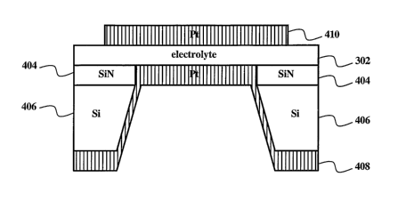
Fig. 4 shows an exemplary fuel cell. A top electrode 410 contacts an
electrolyte 302.
The electrolyte 302 contacts a bottom electrode 408. The electrolyte 302
contacts a substrate.
In this example, the substrate comprise a silicon layer 406 and a top silicon
nitride layer 404.
Figs. 5A-M show an example of a method of malcing a fuel cell on a dense
substrate.
In this example, the electrolyte layer 302 is deposited before the bulk of the
substrate is
etched away.
Fig. 5A show an example substrate. In this example the substrate comprises a
Si layer
406 that has a SiN coating on the top and bottom sides 404, 512. Examples of
thiclcnesses for
the layers are 375 m for the Si layer 406 and 500 nm for SiN layers 404, 512.
It is also
possible to use only Si for the substrate. In that case, it is apparent that
the construction of a
fuel cell would be substantially the same as for the SiN/Si/SiN substrate.
Fig. 5B shows a layer of photoresist 514 deposited on the bottom of the bottom
SiN
CA 02570189 2006-12-13
WO 2006/004957 PCT/US2005/023377
layer 512.
Fig. 5C shows the photoresist 514 exposed to a pattern and developed, which
exposes
part of the bottom SiN layer 512.
Fig. 5D shows a portion of the bottom SiN layer 512 removed by etching.
Fig. 5E shows the example with the photoresist 514 removed from the substrate.
Fig. 5F shows an electrolyte layer 302 deposited on the top SiN layer 404.
Examples
of the thiclmess of the electrolyte layer 302 include a range of 50 to 200 nm.
Fig. 5G shows the example with a layer of photoresist 516 deposited on top of
the
electrolyte layer 302.
Fig. 5H shows the photoresist 516 exposed to a pattern and developed, which
exposes
part of the electrolyte layer 302.
Fig. 5 1 shows a top electrode layer 410 deposited on top of the electrolyte
layer 302
and remainder of the photoresist 516.
Fig. 5J shows remainder of the photoresist 516, and the portion of the
electrode layer
410 that is on top of the photoresist 516, removed.
Fig. 5K shows the Si layer 406 etched.
Fig. 5L shows the remainder of the bottom SiN layer 512 and a portion of the
top SiN
layer 404 etched away. A portion of the electrolyte 302 is now exposed from
the bottom.
Fig. 5M shows a bottom electrode layer 408 deposited. The bottom electrode
layer
408 contacts both the bottom side of the electrolyte 302 and the bottom side
of the Si layer
406. The bottom electrode layer 408 is desirably continuous. It is also
possible to use a Si
substrate. In that case, one would substitute a Si/Si/Si substrate for the
SiN/Si/SiN substrate
as discussed above.
The etching of the substrate to expose the bottom surface of the electrolyte
302 may
occur before or after the deposition of the top electrode layer 410. Atomic
layer deposition
(ALD) may be used to deposit the various layers. A dense electrolyte 302 layer
may be
formed by thin film deposition processes such as DClRF sputtering, chemical
vapor
deposition, pulse laser deposition, molecular beam epitaxy, evaporation and
atomic layer
deposition.
Fig. 6 shows an exemplary image of a porous platinum electrode. The image was
talcen with an electron microscope. One may note the columnar structure of the
Pt. The
spacing seen in Fig. 6 is on the order of 20 nm. The porous nature of the
electrode allows
fuels such as 02 and H2 to reach the electrolyte through the electrode.
Fig. 7 shows an exemplary image of a fuel cell with Pt and YSZ. The image was
11
CA 02570189 2006-12-13
WO 2006/004957 PCT/US2005/023377
talcen with an electron microscope.
Figs. 8A-B show examples of how fuel cells may be grouped on a wafer. An
collection of individual fuel cells 804, one that may be constructed using the
techniques
shown in the Fig. 5 series or the Fig. 6 series, may be arranged in a cell
cluster 802. Each of
the small squares 804 in Fig. 8A represents an individual fuel cell. Only one
is labeled for
clarity. Arranging the fuel cells 804 in a cell cluster 802 allows a large
amount of catalytic
area to be used while retaining the.robust mechanical characteristics of the
substrate 806.
Fig. 8B shows an array of fuel cell clusters 802 arranged in a cluster array
808 on a
substrate 806. Coated and non-coated Si wafers commonly used in
photolithography may be
used as the substrate 806.
Solid ionic conductors usually exhibit high diffusivity and conductivity for
specific
ions, and can be employed as electrolytes in sensors and power sources.
Stabilized zirconia
and doped ceria, in which oxygen ions are the only conductive species, are two
preferred
electrolyte materials for fuel cell and gas sensors. In order to be suitable
for practical
applications, the area specific resistance (ASR) from the electrolyte is
desirably less than 1
ohm per cm2. Since the ASR changes proportionally to the thickness of the
electrolyte, with
an inverse relationship with ionic conductivity, thin solid oxide electrolyte
membranes with
high ionic conductivity will be beneficial to solid-state ionic devices in
order to lower
operating temperatures.
Fig. 11 illustrates exemplary isothermal curves for area specific resistances
of 10 m
and 100 nm thick yttria stabilized zirconia (YSZ) a gadolinia doped ceria
(GDC). It should
be obvious that with a conventional thick YSZ electrolyte membrane (for
example, 10 m
thick), a fuel cell would normally be operated above 700 C. By using 100 nm
YSZ or 100
nm GDC, the operating temperature can be lowered down to 400 C to 200 C,
respectively.
Oxygen ions conduct in ceramics in three modes: within grains, along grain
boundaries, and across grain boundaries. Currently in either doped ceria or
zirconia, the
boundary is considered to be more resistive than the grain interior due to the
existence of a
grain boundary space charge, accumulation of impurities, and segregation at
the boundaries.
The grain boundary conductivity is usually reported to be two to three orders
higher than
grain conductivity. However, these conclusions are all drawn from the
experiments on thick
films which contain at least tens of grain layers as illustrated in Fig. 9.
The blocking effect
may result from crossing grain boundaries. It is desirable to eliminate the
crossing effect by
studying thin GDC films as shown in Fig. 10.
Fig. 9 schematically depicts a solid electrolyte membrane containing cube-like
grains.
12
CA 02570189 2006-12-13
WO 2006/004957 PCT/US2005/023377
The grains are closely paclced in one layer separated by so-called 'along'
grain boundaries
since these grain boundaries are parallel to the ion transport direction.
There are also grains
stacked on top of each other since the thickness of the membrane is much
larger than the
grains. The stacked grains are separated by the so-called 'cross' grain
boundaries as these
grain boundaries are perpendicular to the ion transport direction. In oxygen
ion conductors,
ionic conductivity across grain boundaries (also called grain boundary
conductivity) is
generally lcnown to be two to three orders of magnitude lower than that in the
grains (called
bulk conductivity) at elevated temperature. A thin solid electrolyte membrane
with thickness
comparable to the grain size, as schematically depicted in Fig. 10, is more
beneficial since the
blocking effect from the cross grain boundaries is eliminated.
Fig. 9 shows an electrolyte 906 sandwiched between two electrode layers 902.
There
are multiple grains 904 with corresponding grain boundaries 908. For clarity,
only one of the
grains 904 is labeled. Horizontal grain boundaries 908 are known as 'cross'
grain boundaries,
because migrating ions cross these boundaries in order to travel from one
electrode 902 to
another. Vertical grain boundaries 908 are known as 'along' grain boundaries,
because
migrating ions travel along these boundaries when moving from one electrode
902 to another.
In this example, ions traveling from one electrode 902 to the other cross
multiple grain
boundaries 908 inside the electrolyte 906 thickness.
Fig. 10 shows a thin electrolyte 910 sandwiched between two electrode layers
902. In
this example, ions traveling from one electrode 902 to the other do not cross
multiple grain
boundaries 908 inside the electrolyte 906 thickness. The ions only cross the
grain boundaries
908 that comprise the top and bottom surfaces of the electrolyte.
Experimental data has shown that if the electrolyte layer 910 is equal to or
less than
the average size of grains 904 in the electrolyte 910, then the ion conduction
rate goes up by
one to several orders of magnitude. One may postulate that grain boundaries
908 represent
an iinpedance of migration. Therefore, by reducing the size of the electrolyte
910 such that
the electrolyte 910 comprises a singular plane of grains 904, one or more
orders of magnitude
of ionic conductivity can be gained.
Nano-crystalline ionic conductors will exhibit superior ionic conduction
properties as
described in the following paragraphs. Reducing grain size to tens of
nanometers will
introduce extensive cross grain boundaries in micron or submicron thick
membrane, which is
disadvantageous as depicted above. Hence, the thickness of the electrolyte
membrane is also
desirable to scale down to tens of nanometers.
The solid oxygen-ion conductor has high ionic conductivity based on the defect
13
CA 02570189 2006-12-13
WO 2006/004957 PCT/US2005/023377
chemistry, in which a certain kind of aliovalent dopant, (i.e., a dopant of a
valence different
from that of the host ion) is introduced into the host lattice structure by
substitution and
hence, generates a corresponding amount of oxygen vacancy. These dopants, in
some cases
will tend to segregate to the grain boundary region. Such segregation will
significantly cause
composition redistribution in nano-crystallines and thereby self-generate a
highest ionic
conduction zone in the grain.
Fig. 12 shows the plot of logarithm conductivity as a function of reciprocal
temperature of 500 nm, 100 mn, and 50 nm thick GDC samples, in which grain
size of the in
the range of 20 to 50 nm. The values of ionic conductivity cross grain
boundaries in the 500
nm thick sample (and others above 100 nm) are two orders of magnitude lower
than that
inside the grain. The cross grain boundary conductivity in 100 nm or thinner
film is hardly
observed, which demonstrates that the bloclcing grain boundary resistance is
largely
eliminated. The bulk ionic conductivity in 50 nm or less GDC membrane is one
order of
magnitude higher that that in 100 nm or more GDC membrane due to the dopant
segregation
resulting in an ion highway zone with the highest conductivity.
As the grain size as well as the thickness of the membrane decreases further
to a few
nanometers, space charge layer overlapping is expected and may further enhance
the ionic
conduction.. Maier et al. (Nature, 408(2000), pages 946-949) has presented the
high
conductance performance in CaF2/BaF2 heterostructure. Maier notes that as each
film is thin
enough, the space charge regions overlap each other, the two layers lose their
individuality,
and new conductivity properties fonn. The overlapping region is another type
of self-
generated highway for ion transportation.
Irradiation can generate massive dislocations in the solid oxide electrolyte
membrane.
Since the maximum depth of dislocation region generated by irradiation is
150nm, only in
nano-thin solid electrolyte membrane (less than 150nm), it is possible to have
the dislocation
structures open all the way through the membrane. These artificially-generated
dislocations
may act as ion highways in which ions can transport much faster.
Figs. 14A-C schematically depicts the above three kinds of ion highways in
nano-thin
solid electrolyte membrane whose thickness is comparable to the grain size.
Shown are
electrodes 1402 and electrolyte grains 1404. Each of the figures shows five
grains 1404. For
clarity, only one grain 1404 is labeled.
Fig. 14A shows ion highways 1406 in the grains 1404 self generated by dopant
segregation. Fig. 14A shows five ion highways 1406. For clarity, only one ion
highway
1406 is labeled.
14
CA 02570189 2006-12-13
WO 2006/004957 PCT/US2005/023377
Fig. 14B shows ion highways 1408 in the grains 1404 self generated by space
charge
overlapping. Fig. 14B shows five ion highways 1408. For clarity, only one ion
highway
1408 is labeled.
Fig. 14C shows ion highways 1410 in the grains 1404 induced by irradiation.
Fig.
14C shows five ion highways 1410. For clarity, only one ion highway 1410 is
labeled.
When a fuel cell is working as an electrical power generator, oxygen molecules
are
split into electrons and oxygen ions at the airside before oxygen ions
propagate through the
electrolyte membrane. The reaction rate is another factor that will influence
the fuel cell.
The reaction rate is sometimes referred to in terms of exchange current
density. When the
thickness of electrolyte membrane is reduced to less than 200 nm, it has been
observed that
not only the area specific resistance from electrolyte is reduced as described
above, but that
the reaction rate is also increased by one to two orders of magnitude.
Fig. 13 illustrates calculated fuel cell performances at 350 C when 10 m and
100
nm 8 mole% yttria-stabilized zirconia and 10 mole% gadolinia-doped ceria are
used as a
solid oxide electrolyte. At 350 C the maximum power density using 10 m YSZ
as solid
electrolyte is less than 2 mW/cm2. With fuel cell with a 100 nm YSZ as
electrolyte, the
maximum power density observed is 140 mW/cm2. With the same electrode/catalyst
configuration in a fuel cell with 100 nm GDC as electrolyte, the max power
density is
expected to be 500 mW/cm2. Experimental data (square symbols, which may look
like a very
thick black line when plotted) was obtained by using 50 nm 8% YSZ as a solid
electrolyte
membrane at 350 C on an exemplary fuel cell structure as illustrated in Fig.
4. The
maxiinum power density has reached 130mW/cm2.
Nano-crystalline in nano-thin films may have different surface charge
distributions.
The surface charges may be helpful for gas dissociation combing with the
catalyst and may
promote ion incorporation into the electrolyte lattice. In this way, the
oxygen reaction rate at
the triple phase boundary (gas/catalyst/electrolyte) is faster. Therefore the
catalytic loss is
decreased and the performance of the solid ionic device is further improved.
Thin Film Preparation
The GDC thin films may be prepared by DC-sputtering technique followed by
oxidation in air. The content of an exemplary Cerium/Gadolinium alloy target
(from Kurt J.
Lesker, PA) is 80/20 at% respectively with purity of 99.9%. The target may be
2.00" in
diameter and 0.125" thick. A Si wafer may be selected to be the base substrate
in order to be
CA 02570189 2006-12-13
WO 2006/004957 PCT/US2005/023377
compatible with the state-of-the-art nanotechnology fabrication processes for
later-stage
fabrication of thin film fuel cell. 500nm SiN passivation layer may be grown
on top of the Si
wafer. This SiN layer may be necessary because (i) it is a blocking layer for
wet-etching Si,
which may be necessary in fabrication of micro-SOFC by MEMS technology; (ii)
it is also a
buffer layer which can prevent the reaction between Pt and Si at oxidation and
characterization temperature regime. In order to perform electrochemical
characterization,
200 nm Platinum layer may be sputtered on top of SiN with a 10 nm Titanium
adhesion
layer. Afterwards, Ce/Gd metallic components may be sputtered with controlled
parameters
followed by oxidation at 650 C for 5 hours in air to achieve dense GDC thin
film. Thickness
variation from 50nm to 3 m can be achieved by controlling the sputtering time.
On GDC
films greater than 200 nm thick, a 200 nm Pt electrode may be deposited by DC-
sputtering.
On GDC films less than 200 nm thick, micro Pt electrode can be deposited by
using Focused
Ion Beam (FIB) (from FEI Company).
Morphology
Consider a 50nm thick GDC sample. The film usually comprises grains with a
size of
20-50 nm, which is consistent with AFM (Atomic Force Microscopy) images. From
AFM's
one can observe that the surface is very smooth with only a few nanometers in
height
variation. Cross section images may be obtained by milling with a FIB (Focused
Ion Beam).
The GDC film is relatively dense and the thickness is relatively homogeneous.
Composition
To determine the composition and impurity in the thin film, XPS (X-ray
Photoelectron Spectroscopy) measurements may be perfonned. An exemplary survey
scan of
the sample surface reveals that there is no indication of other elements
except Gd, Ce, 0 and
C, where C is always presented in XPS spectrum. To calculate the ratio of Gd
over Ce, scans
may be accumulated at Ce 3d peak in the range of 870 and 890 eV and Gd 4d peak
in the
range of 130 eV and 150 eV. According to peak area calculations, the atomic
ratio at the
surface between Gd and Ce is around 1:3.7, which is slightly higher than the
alloy
composition 1:4. Segregation of the Gd to the surface is one well-
known,reason, and the
accuracy of the area calculation is another one. After etching of a few
seconds from the
surface layer by argon ion bombardment, the Gd/Ce ratio is close to the
nominal composition
1:4. An example of an Argon ion bombarding rate is around 0.2 nm/sec at the
current to 10
mA on the feature area of 1 mm2. The accumulated of Ce 3d, Ols, and Pt 4f
spectra may be
16
CA 02570189 2006-12-13
WO 2006/004957 PCT/US2005/023377
recorded periodically (every 50 seconds for example) in order to monitor the
composition and
hence homogeneity of the film.
The depth of the layer can also be estimated from the depth profile when the
Pt peak
appears in the spectra. One may see a depth profile of Ce 3d, Ols and Pt 4f.
No significant
changes of the Ce 3d peak in position and width are possible, indicating the
homogeneity of
fully oxidized Ce. After etching for a duration (1050 seconds for example),
the peak of Ce
may completely disappear and the pealc corresponding to Pt 4f may show up. The
thickness
of the ceria layer can be estimated by multiplying the etching time and the
etching rate.
Hence, the tliiclcness of the thin film, given the example parameters above,
is around 210 nm,
which is consistent with observation of SEM/FIB pictures.
Electrochemical Characterization
In order to exclude any surface effect on the results, one may perform the
direct
electrochemical measurements in a cross configuration, as illustrated in Fig.
15. AC
impedance and DC polarization data may be obtained from a Solartron 1287/1260
system.
To avoid pinholes in the thin film, a micro Pt electrode may be patterned on
by FIB. There
are at least two possible ways for patterning: (a) direct depositing by FIB,
and (b) sputtering
large area with Pt and then milling off by FIB. The quality of Pt will be
different. Around
50% carbon are contained in the Pt pattern by direct deposition. Micro probes
may be used
as electrical connectors.
Fig. 15 shows an exemplary dense Pt electrode, GDC electrolyte, and dense Pt
electrode coinbination for electrochemical characterization. A substrate may
be made out of
a Si wafer 1502 that has a top SiN coating layer 1504 and a bottom SiN coating
layer 1506.
A titanium layer 1508 may be deposited to aid adllesion between the dense Pt
layer 1510 and
the SiN layer 1504. A GDC electrolyte layer 1512 is deposited on the dense Pt
layer 1510.
A Pt layer 1514 is deposited on the GDC electrolyte layer 1512. The layers may
be deposited
such that a current source 1516 can access the Pt layers 1510, 1514. The SiN
layers may
optionally be omitted.
DC characteristics
The polarization profile of a Pt/GDC (1 m)/Pt system may be obtained at the
room
temperature and 300 C. Positive as well as negative polarization voltages
with a value of 50
mV may be applied. An exponential current drop may be observed. At room
temperature,
the initial current was observed to be around 1e-8 A and after 2500 seconds,
the current
17
CA 02570189 2006-12-13
WO 2006/004957 PCT/US2005/023377
stabilized in the range of 4e-10 A. As both electrodes are ionic blocking
electrode at room
temperature, the remained current may be due to the electronic conductance in
the electrolyte
and/or due to the limitation of the instrument. The ionic transference number
can be
estimated according to the following equation, t = 1- I./I , where I. and I
are the currents
measured at the equilibrium time and the beginning, respectively. Hence, the
ionic
transference number of our GCO thin film at room temperature and 300 C was
observed to
be greater than 0.98 and 0.96 respectively.
One may also measure the cyclic voltammetry profiles at room temperature. The
scan
rate may vary from lm V/s to 0.1 mV/s and the scan window may be set to + 0.8
and -0.8 V
vs. the counter Pt electrode. The current may start to increase at 0.75 V,
indicating an
ongoing reaction process. This may be due to the adsorbed water deposition.
The thin film
after CV measurement was subjected to impedance measurement again and no
changes of the
conductance were found, indicating that the thin film and GDC were stabilized
in the
potential region. Thus, the prepared GDC thin film is suitable to work as an
oxygen ionic
conductance within 1 V voltage at room atmosphere.
AC iinpedance Analyses
Impedance spectra may be recorded in air upon increasing temperatures from 100
C
up to 350 C on the thin films with various thicknesses. Impedance data may be
retrieved by
fitting the spectra using Z-view software based on non-linear least square
method. Typical
Cole-Cole plots may be obtained from samples with various thicknesses at 150
C. For a
700nm thick sample, the plot may be fitted with two semicircles corresponding
to bulk and
grain boundary resistance. By decreasing the thickness, the resistance
corresponding to grain
conductance may be observed to decrease significantly and become invisible for
a 50nm
thick sample.
The conductivity of thin film GDC may be plotted as a functional temperature
and
activation energy (Ea) calculated from a slope changing trend with the
thickness of the film.
One may note that ionic conduction behaves differently in different thickness
regimes. Films
thicker than 1 m exhibit conventional impedance spectia with two arcs
corresponding to
bulk and cross grain boundary conductance with activation energy of 0.7 and
0.85 eV,
respectively. The cross grain boundary conductivity was observed to be two
orders of
magnitude lower than bulk conductivity, indicating the significant blocking.
As the thickness
decreases, the grain boundary conductivity increased to the bullc conductivity
level with
activation energy was observed to decrease to 0.6 eV. Beyond 100 nm only one
arc was
18
CA 02570189 2006-12-13
WO 2006/004957 PCT/US2005/023377
observed in the impedance spectra. The conductivity was observed to be around
one order of
magnitude higher than bulk conductivity and the activation energy kept at 0.6
eV.
The improvements by using nano-thin solid electrolyte membranes can be the
results
of reducing the resistance loss from the electrolyte due to the decrease of
the membrane
thickness and/or due to the increase of the ionic conductivity that occurs
when the membrane
thiclcness is comparable to the grain size. The increased ionic conductivity
can be the results
of elimination of cross grain boundaries and/or containing special ion
highways for
transportation resulting from the segregation of the dopants, space charge
overlapping, and
irradiation-induced dislocations.
The improvements by using such nano-thin solid electrolyte membrane can also
be
the results of reducing the catalytic losses from charge transport reactions
that occur at
gas/electrode/electrolyte triple phase boundaries due to the special
distribution of the surface
charges as well as electric fields.
It will be apparent to one skilled in the art that the described embodiments
may be
altered in many ways without departing from the spirit and scope of the
invention.
Accordingly, the scope of the invention should be determined by the following
claims and
their equivalents.
19