Note: Descriptions are shown in the official language in which they were submitted.
CA 02570308 2006-12-14
WO 2006/007203 PCT/US2005/018538
Nanotube-based Logic Driver Circuits
Cross-Reference to Related Applications
[0001] This application claims priority under 35 U.S.C. 119(e) to U.S.
Provisional Pat. Apl., Ser. 60/581,074, filed on June 18, 2004, entitled
Nonvolatile
Carbon Nanotube Logic (NLOGIC) Off Chip Driver, which is incorporated herein
by
reference in its entirety.
[0002] This application is related to the following references:
U.S. Pat. Apl. Ser. No. 10/917,794, filed on August 13, 2004, entitled
Nanotube-Based Switching Elements;
U.S. Pat. Apl. Ser. No. 10/918,085, filed on August 13, 2004, entitled
Nanotube-Based Switching Elements With Multiple Controls;
U.S. Pat. Apl. Ser. No. 10/918,181, filed on August 13, 2004, entitled
Nanotube Device Structure And Methods Of Fabrication;
U.S. Pat. Apl. Ser. No. 10/917,893, filed on August 13, 2004, entitled
Nanotube-Based Switching Elements And Logic Circuits;
U.S. Pat. Apl. Ser. No. 10/917,606, filed on August 13, 2004, entitled
Isolation Structure For Deflectable Nanotube Elements;
U.S. Pat. Apt. Ser. No. 10/917,932, filed on August 13, 2004, entitled
Circuits Made From Nanotube-Based Switching Elements With Multiple
Controls;
U.S. Pat. Apl. Ser. No. not yet assigned, filed on date even herewith
entitled, Nanotube-Based Transfer Devices and Related Circuits;
U.S. Pat. Apl. Ser. No. not yet assigned, filed on date even herewith
entitled, Integrated Nanotube and Field Effect Switching Device;
U.S. Pat. Apl. Ser. No. not yet assigned, filed on date even herewith
entitled, Receiver Circuit Using Nanotube-Based Switches and
Transistors;
U.S. Pat. Apl. Ser. No. not yet assigned, filed on date even herewith
entitled, Receiver Circuit Using Nanotube-based Switches and Logic;
U.S. Pat. Apl. Ser. No. not yet assigned, filed on date even herewith
entitled, Storage Elements Using Nanotube Switching Elements; and
U.S. Pat. Apl. Ser. No. not yet assigned, filed on date even herewith
entitled, Tri-State Circuit Using Nanotube Switching Elements.
CA 02570308 2009-12-09
69675-802
Nanotube-based Logic Driver Circuits
Background
1. Technical Field
[0003] The present application generally relates to nanotube switching
circuits
and in particular to nanotube switching circuits used in driver circuits
capable of
driving relatively high capacitive loads.
2. Discussion of Related Art
[0004] Digital logic circuits are used in personal computers, portable
electronic,
devices such as personal organizers and calculators, electronic entertainment
devices,
and in control circuits for appliances, telephone switching systems,
automobiles,
aircraft and other items of manufacture. Early digital logic was constructed
out of
discrete switching elements composed of individual bipolar transistors. With
the
invention of the bipolar integrated circuit, large numbers of individual
switching
elements could be combined on a single silicon substrate to create complete
digital
logic circuits such as inverters, NAND gates, NOR gates, flip-flops, adders,
etc.
However, the density of bipolar digital integrated circuits is limited by
their high
power consumption and the ability of packaging technology to dissipate the
heat
produced while the circuits are operating. The availability of metal oxide
semiconductor ("MOS") integrated circuits using field effect transistor
("FET")
switching elements significantly reduces the power consumption of digital
logic and
enables the construction of the high density, complex digital circuits used in
current
technology. The density and operating speed of MOS digital circuits are still
limited
by the need to dissipate the heat produced when the device is operating.
1
CA 02570308 2009-12-09
69675-802
[0005] Digital logic integrated circuits constructed from bipolar or MOS
devices
do not function correctly under conditions of high heat or heavy radiation.
Current
digital integrated circuits are normally designed to operate at temperatures
less than
100 degrees centigrade and few operate at temperatures over 200 degrees
centigrade.
In conventional integrated circuits, the leakage current of the individual
switching
elements in the "off' state increases rapidly with temperature. As leakage
current
increases, the operating temperature of the device rises, the power consumed
by the
circuit increases, and the difficulty of discriminating the off state from the
on state
2
CA 02570308 2006-12-14
WO 2006/007203 PCT/US2005/018538
reduces circuit reliability. Conventional digital logic circuits also short
internally
when subjected to heavy radiation because the radiation generates electrical
currents
inside the semiconductor material. It is possible to manufacture integrated
circuits
with special devices and isolation techniques so that they remain operational
when
exposed to heavy radiation, but the high cost of these devices limits their
availability
and practicality. In addition, radiation hardened digital circuits exhibit
timing
differences from their normal counterparts, requiring additional design
verification to
add radiation protection to an existing design.
[0006] Integrated circuits constructed from either bipolar or FET switching
elements are volatile. They only maintain their internal logical state while
power is
applied to the device. When power is removed, the internal state is lost
unless some
type of non-volatile memory circuit, such as EEPROM (electrically erasable
programmable read-only memory), is added internal or external to the device to
maintain the logical state. Even if non-volatile memory is utilized to
maintain the
logical state, additional circuitry is necessary to transfer the digital logic
state to the
memory before power is lost, and to restore the state of the individual logic
circuits
when power is restored to the device. Alternative solutions to avoid losing
information in volatile digital circuits, such as battery backup, also add
cost and
complexity to digital designs.
[0007] Important characteristics for logic circuits in an electronic device
are low
cost, high density, low power, and high speed. Resistance to radiation and the
ability
to function correctly at elevated temperatures also expand the applicability
of digital
logic. Conventional logic solutions are limited to silicon substrates, but
logic circuits
built on other substrates would allow logic devices to be integrated directly
into many
manufactured products in a single step, further reducing cost.
[0008] Devices have been proposed which use nanoscopic wires, such as single-
walled carbon nanotubes, to form crossbar junctions to serve as memory cells.
(See
WO 01/03208, Nanoscopic Wire-Based Devices, Arrays, and Methods of Their
Manufacture; and Thomas Rueckes et al., "Carbon Nanotube-Based Nonvolatile
Random Access Memory for Molecular Computing," Science, vol. 289, pp. 94-97, 7
July, 2000.) Hereinafter these devices are called nanotube wire crossbar
memories
(NTWCMs). Under these proposals, individual single-walled nanotube wires
3
CA 02570308 2009-12-09
69675-802
suspended over other wires define memory cells. Electrical signals are written
to one
or both wires to cause them to physically attract or repel relative to one
another. Each
physical state (i.e., attracted or repelled wires) corresponds to an
electrical state.
Repelled wires are an open circuit junction. Attracted wires are a closed
state forming
a rectified junction. When electrical power is removed from the junction, the
wires
retain their physical (and thus electrical) state thereby forming a non-
volatile memory
cell.
[0009] U.S. Patent Publication No. 2003-0021966 discloses, among other things,
electromechanical circuits, such as memory cells, in which circuits include a
structure
having electrically conductive traces and supports extending from a surface of
a
substrate. Nanotube ribbons that can electromechanically deform, or switch are
suspended by the supports that cross the electrically conductive traces. Each
ribbon
comprises one or more nanotubes. The ribbons are typically formed from
selectively
removing material from a layer or matted fabric of nanotubes.
[0010] For example, as disclosed in U.S. Patent Publication No. 2003-0021966,
a
nanofabric may be patterned into ribbons, and the ribbons can be used as a
component
to create non-volatile electromechanical memory cells. The ribbon is
electromechanically-deflectable in response to electrical stimulus of control
traces
and/or the ribbon. The deflected, physical state of the ribbon may be made to
represent a corresponding information state. The deflected, physical state has
non-
volatile properties, meaning the ribbon retains its physical (and therefore
informational) state even if power to the memory cell is removed. As explained
in
U.S. Patent Publication No. 2003-0124325, three-trace architectures may be
used for
electromechanical memory cells, in which the two of the traces are electrodes
to
control the deflection of the ribbon.
[0011] The use of an electromechanical bi-stable device for digital
information
storage has also been suggested (c.f. US4979149: Non-volatile memory device
including a micro-mechanical storage element).
[0012] The creation and operation of bi-stable, nano-electro-mechanical
switches
based on carbon nanotubes (including mono-layers constructed thereof) and
metal
electrodes has been detailed in a previous patent application of Nantero, Inc.
4
CA 02570308 2009-12-09
69675-802
(See for example Patent Nos. 6574130, 6643165, 6706402, 6919592, 6911682,
6784028, 6835591, 7566478, 7560136, 7335395, 7259410, and 6924538).
Summary
[0013] The invention provides nanotube based logic driver circuits. These
include pull-up driver circuits, push-pull driver circuits, tristate driver
circuits, among
others.
[0014] Under one aspect of the invention, an off-chip driver circuit includes
a
differential input having a first and second signal links, each coupled to a
respective
one of two differential, on-chip signals. At least one output link is
connectable to an
off-chip impedance load, and at least one switching element has an input node,
an
output node, a nanotube channel element, and a control structure disposed in
relation
to the nanotube channel element to controllably form and unform an
electrically
conductive channel between said input node and said output node. The input
node is
coupled to a reference signal and the control structure is coupled to the
first and
second signal links. The output node is coupled to the output link, and the
nanotube
channel element is sized to carry sufficient current to drive said off-chip
impedance
load.
[0015] Under another aspect of the invention, the output link is coupled to a
pull-
up resistive load coupled to -a supply voltage.
[0016] Under another aspect of the invention, the supply voltage coupled to
the
resistive load is different than the supply voltage of a chip having the off
chip driver
circuit.
[0017] Under another aspect of the invention, the off-chip driver circuit
further
includes a second switching element having an input node, an output node, a
nanotube
channel element, and a control structure disposed in relation to the nanotube
channel
element to controllably form and unform an electrically conductive channel
between
said input node and said output node; and further comprising a second output
link
connectable to a second off-chip impedance load. The input node of the second
CA 02570308 2006-12-14
WO 2006/007203 PCT/US2005/018538
switching element is coupled to a reference signal and the control structure
of the
second switching element is coupled to the first and second signal links. The
output
node of the second switching element is coupled to the second output link, and
the
nanotube channel element of the second switching element is sized to carry
sufficient
current to drive the off-chip impedance load.
[0018] Under another aspect of the invention, an off-chip driver circuit
includes a
differential input having a first and second signal links, each coupled to a
respective
one of two differential, on-chip signals. At least one output link is
connectable to an
off-chip impedance load. At least first and second switching elements each
have an
input node, an output node, a nanotube channel element, and a control
structure
disposed in relation to the nanotube channel element to controllably form and
unform
an electrically conductive channel between said input node and said output
node. The
input node of the first switching element is coupled to a first reference
signal and
input node of the second switching element is coupled to a second reference
signal.
The control structure of each of the first and second switching elements is
coupled to
the first and second signal links and the output node of each of the first and
second
switching elements is coupled to the output link. The nanotube channel element
of
each of the first and second switching elements is sized to carry sufficient
current to
drive said off-chip impedance load.
[0019] Under another aspect of the invention, an off-chip driver circuit
includes a
differential input having a first and second signal links, each coupled to a
respective
one of two differential, on-chip signals. First and second output links are
each
connectable to an off-chip impedance load. The circuit further includes at
least first
and second push-pull drivers, each push-pull driver connected to the first and
second
input links and each connected to a respective one of the first and second
output links.
Each push-pull driver includes first and second switching elements, each
having an
input node, an output node, a nanotube channel element, and a control
structure
disposed in relation to the nanotube channel element to controllably form and
unform
an electrically conductive channel between said input node and said output
node. The
input node of the first switching element is coupled to a first reference
signal and
input node of the second switching element is coupled to a second reference
signal.
The control structure of each of the first and second switching elements is
coupled to
6
CA 02570308 2006-12-14
WO 2006/007203 PCT/US2005/018538
the first and second signal links and the output node of each of the first and
second
switching elements is coupled to a respective one of the output links. The
nanotube
channel element of each of the first and second switching elements is sized to
carry
sufficient current to drive said off-chip impedance load.
[0020] Under another aspect of the invention, an off-chip tristate driver
circuit
includes a differential input having a first and second signal links, each
coupled to a
respective one of two differential, on-chip signals. At least one output link
is
connectable to an off-chip impedance load. The circuit includes at least first
and
second switching elements, each having an input node, an output node, a
nanotube
channel element, and a control structure disposed in relation to the nanotube
channel
element to controllably form and unform an electrically conductive channel
between
said input node and said output node. The control structure of each of the
first and
second switching elements is coupled to the first and second signal links and
the
output node of each of the first and second switching elements is coupled to
the
output link. The nanotube channel element of each of the first and second
switching
elements is sized to carry sufficient current to drive said off-chip impedance
load.
The input node of the first switching element is coupled to a first reference
signal
through a first selection structure and the input node of the second switching
element
is coupled to a second reference signal through a second selection structure.
[0021] Under another aspect of the invention, the first and second selection
structures are each switching elements having an input node connected to a
respective
one of the first and second reference signals, an output node connected to a
respective
input node of the first and second switching elements, a nanotube channel
element,
and a control structure disposed in relation to the nanotube channel element
to
controllably form and unform an electrically conductive channel between said
input
node and said output node, and the control structure is coupled of each
selection
structure is coupled to at least one selection signal.
Brief Description of the Drawings
[0022] Figure 1 is a transverse cross-sectional view of a nanotube in relation
to a
substrate;
[0023] Figure 2 is a plan view of two separated nanotubes;
7
CA 02570308 2006-12-14
WO 2006/007203 PCT/US2005/018538
[0024] Figure 3 is a plan view of a plurality of nanotubes suspended by
contacts;
[0025] Figure 4A is a single rail driver circuit according to certain
embodiments;
[0026] Figure 4B is a dual rail driver circuit according to certain
embodiments;
[0027] Figure 5 depicts a pre-driver circuit that may be used in conjunction
with a
driver circuit according to certain embodiments of the invention;
[0028] Figures 6A-D depict a preferred nanotube switching element in cross-
section and layout views and in two informational states;
[0029] Figures 7A-C depict the notation used to describe the nanotube switch
and
its states;
[0030] Figure 8 depicts a single rail, push pull driver circuit according to
certain
embodiments;
[0031] Figure 9 depicts a dual rail, push pull driver circuit according to
certain
embodiments;
[0032] Figure 10 depicts a single rail, tristate, push pull driver circuit
according to
certain embodiments; and
[0033] Figure 11 depicts a dual rail, tristate, push pull driver circuit
according to
certain embodiments.
8
CA 02570308 2006-12-14
WO 2006/007203 PCT/US2005/018538
Detailed Description
[0034] Preferred embodiments of the invention arrange nanotube-based switches
into driver circuits capable of driving relatively large capacitances, such as
off chip
(OC) capacitances, long or heavily loaded interconnect lines, etc. The
circuits may be
either dual-rail (differential) or single-rail, open carbon nanotube (CNT)
output
(corresponds to open drain in an FET), push pull drivers, and tristate push
pull
drivers, for example.
[0035] Carbon nanotube-based logic circuits, such as those circuits disclosed
in
the incorporated, related references, may be required to drive a relatively
large
capacitance, 10 pf for example, when driving off-chip, or when driving heavy
loads
on-chip. Nanotube-based logic circuits using porous carbon nanotube fabrics to
construct nanotube channel elements are typically low capacitance circuits,
e.g., 30 aF
(0.030 fF) input and output capacitances, and can typically drive only
relatively low
capacitances. Preferably, a logic family includes circuits that can drive
large
capacitive loads, such as 10 pf.
[0036] Figure 1 depicts in transverse cross-sectional view of a single
nanotube 15
(e.g., carbon nanotube) of diameter 2R (typically 0.6 to 1.5 nm in diameter)
and
height h above a conductive region 20, where the conductive region is
typically a
control (or set) or a release electrode, such as disclosed in the
incorporated, related
references.
[0037] Figure 2 illustrates a plan view of two nanotube fibers 15 of diameter
2R
and a void region XVOID between fibers in the porous nanotube fabric layer.
[0038] Figure 3 illustrates a plan view of multiple carbon nanotubes, labeled
15a-
n of length LSUSP. The CNTs are suspended between NT contact conductors 40 to
form the nanotube channel elements of exemplary carbon nanotube switches, such
as
those disclosed in the incorporated, related references. In this figure, the
nanotubes
are depicted as if they are aligned in parallel, but in preferred embodiments
such
alignment is not necessary and in many embodiments such strict parallel
alignment is
not expected. As described in the incorporated references, LSUSP for a modern
implementation may be about 325 nm (0.325 gm), for example.
9
CA 02570308 2006-12-14
WO 2006/007203 PCT/US2005/018538
[0039] Present nanotube fabric densities may be approximately 10 nanotubes in
a
200 x 200 nm region. A 325 x 325 nm region comprising a suspended length LSUSP
= 325 nm and width = 325 nm contains approximately 15 NTs, for example. XVOID
may be calculated using the equation 15(2R + XVOID) = 325 nm, where 2R = 1.5
nm, for example. XVOID is approximately equal to 20 nm, for example. For 2R =
1.5 nm, and XVOID = 20 nm, the nanotube fabric density is approximately 7% NTs
with a 93% void region. In operation, the NT fibers are in contact with the
insulator
layer of a control or release electrodes (with a conductive element under the
insulator
layer). The control or release electrode conductor approximates ground plane
20
shown in figure 1.
[0040] Capacitance between the nanotube and the control or release electrodes
is
contributed by an approximately 65 nm portion of NT fiber length in close
proximity
to the electrodes. The insulator thickness is assumed to be approximately 15
nm (h =
15 nm as shown in figure 1), and the dielectric is assumed to be Si02 with
relative
dielectric constant of approximately 4. The capacitance per nanotube is
calculated
using the following equation:
C = l/cosh-1(1 + h/R), where cosh-1 = irsllln [(1 + h/R) + {(l+h/R)2 -
1}0.5 ]
as given in Ramo, S. and Whinnery, J. R., Fields and Waves in Modern Radio,
John
Wiley and Sons, 1958 138-14. For 15 nanotubes in parallel, the nanotube
electrostatic
switch input capacitance is 30 aF (0.030 fF). Output capacitance and local
wiring
capacitance is estimated as also 30 aF.
[0041] The resistance of a nanotube nonvolatile electrostatic switch consists
of a
conductor to nanotube contact resistance Re in series with a nanotube to
output
electrode conductor contact resistance (when the switch is in the "ON" state)
of RSW.
Nanotube switches (e.g., non-volatile) are typically symmetrical, and Rc
consists of
two contacts in parallel. RSW also uses two contacts in parallel. Each
conductor to
nanotube contact is approximately 20,000 Ohms, for example, and each switching
contact is approximately 30,000 Ohms, for example. The total resistance
between the
nanotube contacts and the output contacts is approximately 25,000 Ohms per
nanotube, for example. The resistance is dominated by contact resistance, so
that the
CA 02570308 2006-12-14
WO 2006/007203 PCT/US2005/018538
nanotube fiber resistance is negligible. For 15 parallel nanotubes, the
nanotube
resistance is approximately 1,700 ohms.
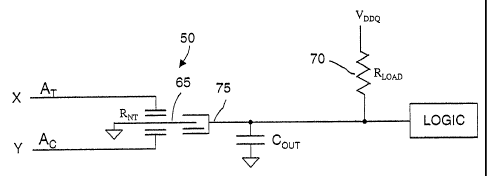
[0042] Figure 4A illustrates a nanotube nonvolatile off chip driver (OCD) 50.
The
term off chip driver is used to refer to a circuit driving a heavy capacitive
load, such
as 10 pF for example, whether the load is on the same chip or on another chip.
Driver
50 includes nanotube switching element 65 (more below) connected to output
terminal 75 and drives a capacitive load COUT, and a pull-up resistor RLOAD
70(COUT and RLOAD are not part of output driver 50) connected to power supply
voltage VDDQ. The driver 50 is coupled to a logic circuit (a receiver, for
example).
Nanotube switching element 65 is driven by the outputs of a predriver stage at
terminals X and Y, with true and complementary logic inputs AT and AC,
respectively. The output 75 of nanotube switching element 65 is connected to
capacitive load COUT, pull-up resistor RLOAD, and a logic input. The nanotube
channel element (more below) is connected to ground as a reference via a
signal
electrode (more below when describing an exemplary nanotube switching
element).
Preferred embodiments form switching element 65 such that the nanotube channel
element has a number of nanotubes to provide a resistance RNT between output
and
ground of approximately 60 Ohms. A switch with 15 nanotubes in parallel has a
resistance of 1,700 Ohms, an input capacitance of approximately 30 aF (0.030
fF),
and occupies a width of 302.5 nm (approximately 0.30 um). A switch with 425
parallel nanotubes has a resistance of approximately 60 ohms, an input
capacitance of
approximately 850 aF (0.85 fF), and occupies a width of 9,117.5 nm
(approximately
9.12 um). The capacitance load COUT is approximately 10 pF, for example. The
pull-up resistor RLOAD must be much larger than RNT, and is selected as 600
ohms,
for example.
[0043] In operation, if input AT is at a positive voltage and AC is at ground,
switching element 65 is turned "ON" (CLOSED), and output 75 is connected to
ground through a 60 Ohm resistance (of the switch 65) discharging capacitor
COUT.
If COUT = 10 pF, the discharge time constant RNTCOUT is approximately 600 ps,
and the output fall time is less than 1.5 ns. Note that as long as output 75
is held at
ground, a dc current will flow from power source VDDQ through resistor 70 and
driver 65 to ground. The dc current is a consequence of the open-CNT output
design,
11
CA 02570308 2006-12-14
WO 2006/007203 PCT/US2005/018538
corresponding to an open-drain FET design and will be discussed further below.
Note
that output drivers are often powered by a dedicated power bus at a voltage
referred to
as VDDQ and other circuits in the chip by a separate power bus referred to as
VDD in
order to minimize on-chip-noise when switching large output driver circuits.
VDDQ
may be the same voltage as VDD or may be at a higher or lower voltage than
VDD.
Examples of VDD and VDDQ and are 5, 3.3, 2.5, and 1.8 volts.
[0044] In operation, if input AT is at zero volts and AC is a positive
voltage,
switch 65 is turned "OFF" (OPEN), and node 75 voltage rises to VDDQ as
resistor
RLOAD charges capacitor COUT. The charge time constant RLOADCOUT is 6 ns,
and the output rise time is less than 15 ns. No dc current flows when output
node 75
is in the open state.
[0045] The voltage applied to driver input terminals X and Y does not have to
be
equal to VDDQ. The driver input voltages applied to terminals X and Y may be
1.5
volts, for example, and VDDQ may be 3.3 volts, for example. Driver 50 may be
used
to drive a broad range of VDDQ voltage levels, from less than 1 volt to
greater than 5
volts, for example.
[0046] Figure 4B illustrates a dual-rail output driver 80. The circuit 80
includes
nanotube switching elements 85 and 90, interconnected as shown, and has dual-
rail
(differential) inputs X and Y and dual-rail (differential) outputs 95 and 95'.
Each
output drives a capacitance load COUT, a resistor RLOAD, and a logic input.
Each
switching element 85 and 90 is sized as described above to provide appropriate
drive
(e.g., wide enough to have 425 nanotubes in parallel), and has an "ON"
resistance of
about 60 Ohms. The input capacitance at inputs X and Y is approximately 0.85
fF.
The operation of nanotube switching elements 85 and 90 shown in figure 4B is
the
same as the operation of nanotube switch 65 shown in figure 4A and described
earlier.
[0047] Output driver 50 and output driver 80 each require a pre-driver
amplification stage. The output drivers use nanotube switches with 425
parallel
nanotubes with an input capacitance of 0.85 fF, while logic in this example
typically
uses nanotube switches with 15 parallel nanotubes, having an input capacitance
of
0.030 M. A pre-driver is used to drive output drivers 50 and 80. A pre-driver
consists
of a chain (several stages) of nanotube inverters of increasing size. The pre-
driver
12-
CA 02570308 2006-12-14
WO 2006/007203 PCT/US2005/018538
uses enough stages so that the last pre-driver stage is strong enough to drive
the input
capacitance of the nanotube output driver. It is well known (G.E. Sobelman,
"Advanced Digital Circuit Design", EE course printed notes, copyright 2001",
pages
9 - 15, and H.B. Bakoglu, "Circuits, interconnections, and Packaging for
VLSI",
Addison-Wesley Publishing Co., 1990, pages 172 - 173) that in order to
minimize the
total delay along a pre-driver path, each pre-driver stage should carry
approximately
the same load, typically expressed as the same COUT/CIN capacitance ratio at
each
stage, with COUT/CIN in the 3 to 5 range.
[0048] Figure 5 illustrates nanotube-based three-stage pre-driver 100. Each
stage
is composed of a dual-rail (differential) nanotube nonvolatile inverter logic
stage with
input and output loads indicated as C1- C4. The operation of dual-rail
nanotube
inverters is described in some of the incorporated, related references. The
outputs X
and Y of pre-driver 100 connect to inputs X and Y of driver 50 in figure 4A
and
driver 80 of figure 4B. Capacitance C4 is 0.85 fF, i.e., the input capacitance
of OCD
50 or OCD 80. Capacitance Cl is the input capacitance 0.030 fF of a 15 NT
nanotube
switch. Selecting a COUT/CIN design ratio of 3, the NT switches in pre-driver
100
stages 1- 3 and OCD 50 or 80 are summarized in Table 1.
Stage 1 Stage 2 Stage 3 OCD
# NTs in parallel 15 45 135 425
# NTs Ratio (relative to stage 1) 1 3 9 28
CIN (fF) 0.03 0.09 0.27 0.85
COUT (F) 0.09 0.27 0.85 10,000*
NT Switch Lsusp ( m) 0.325 0.325 0.325 0.325
NT Switch Width ( m) 0.325 0.975 2.925 8.775
* 10 pf load driven by the OCD using a load pull-up approach shown in figure
4A&B
Table 1
[0049] Table 1 shows the NT switch characteristics used at each of the three
pre-
amplifier 100 stages, stage 1, stage 2, and stage 3. Table 1 also shows the
characteristics of the OCD NT output driver (switch) 50 and 80. The load pull-
up
approach enables an nanotube switching element based OCD to discharge a large
10
pF capacitance, and therefore to drive a large capacitive load directly from
an NT
switch. However, the fall time is much faster than the rise time
(approximately
1/10th) and dc current flows when the driver output node is at ground.
13
CA 02570308 2006-12-14
WO 2006/007203 PCT/US2005/018538
[0050] Figures 6A-D depict a preferred nanotube switching element 600 in cross-
section and layout views and in two informational states. These switches may
be used
for switches 65, 85 or 90 of figures 4A-B. A more detailed description of
these
switches may be found in the related cases identified and incorporated above.
A brief
description follows here for convenience.
[0051] Figure 6A is a cross sectional view of a preferred nanotube switching
element 100. Nanotube switching element includes a lower portion having an
insulating layer 117, control electrode 111, output electrodes 113c,d.
Nanotube
switching element further includes an upper portion having release electrode
112,
output electrodes 113a,b, and signal electrodes 114a,b. A nanotube channel
element
115 is positioned between and held by the upper and lower portions.
[0052] Release electrode 112 is made of conductive material and is separated
from nanotube channel element 115 by an insulating material 119. The channel
element 115 is separated from the facing surface of insulator 119 by a gap
height
G102.
[0053] Output electrodes 113a,b are made of conductive material and are
separated from nanotube channel element 115 by insulating material 119.
[0054] Output electrodes 113c,d are likewise made of conductive material and
are
separated from nanotube channel element 115 by a gap height G103. Notice that
the
output electrodes 11 3c,d are not covered by insulator.
[0055] Control electrode 111 is made of conductive material and is separated
from nanotube channel element 115 by an insulating layer (or film) 118. The
channel
element 115 is separated from the facing surface of insulator 118 by a gap
height
G104.
[0056] Signal electrodes 114a,b each contact the nanotube channel element 115
and can therefore supply whatever signal is on the signal electrode to the
channel
element 115. This signal may be a fixed reference signal (e.g., VDD or Ground)
or
varying (e.g., a Boolean discrete value signal that can change). Only one of
the
electrodes 1 14a,b need be connected, but both may be used to reduce effective
resistance.
14
CA 02570308 2006-12-14
WO 2006/007203 PCT/US2005/018538
[0057] Nanotube channel element 115 is a lithographically-defined article made
from a porous fabric of nanotubes (more below). It is electrically connected
to signal
electrodes 1 14a,b. The electrodes 1 14a,b and support 116 pinch or hold the
channel
element 115 at either end, and it is suspended in the middle in spaced
relation to the
output electrodes 113a-d and the control electrode 111 and release electrode
112.
The spaced relationship is defined by the gap heights G102-G104 identified
above.
For certain embodiments, the length of the suspended portion of channel
element 115
is about 300 to 350 nm.
[0058] Under certain embodiments the gaps G103, G104, G102 are in the range of
- 30 nm. The dielectric on terminals 112, 111, and 1 13a and 113b are in the
range
of 5 - 30 nm, for example. The carbon nanotube fabric density is approximately
10
nanotubes per 0.2 x 0.2 um area, for example. The suspended length of the
nanotube
channel element is in the range of 300 to 350 nm, for example. The suspended
length
to gap ratio is about 5 to 15 to 1 for non-volatile devices, and less than 5
for volatile
operation, for example.
[0059] Figure 6B is a plan view or layout of nanotube switching element 100.
As
shown in this figure, electrodes 113b,d are electrically connected as depicted
by the
notation `X' and item 102. Likewise electrodes 113a,c are connected as
depicted by
the X. In preferred embodiments the electrodes are further connected by
connection
120. All of the output electrodes collectively form an output node 113 of the
switching element 100.
[0060] Under preferred embodiments, the nanotube switching element 100 of
figures 6A and 6B operates as shown in figures 6C and D. Specifically,
nanotube
switching element 100 is in an OPEN (OFF) state when nanotube channel element
is
in position 122 of figure 6C. In such state, the channel element 115 is drawn
into
mechanical contact with dielectric layer 119 via electrostatic forces created
by the
potential difference between electrode 112 and channel element 115. Output
electrodes 113a,b are in mechanical contact (but not electrical contact) with
channel
element 115. Nanotube switching element 100 is in a CLOSED (ON) state when
channel element 115 is elongated to position 124 as illustrated in figure 6D.
In such
state, the channel element 115 is drawn into mechanical contact with
dielectric layer
118 via electrostatic forces created by the potential difference between
electrode 111
CA 02570308 2006-12-14
WO 2006/007203 PCT/US2005/018538
and channel element 115. Output electrodes 113c,d are in mechanical contact
and
electrical contact with channel element 115 at regions 126. Consequently, when
channel element 115 is in position 124, signal electrodes 1 14a and 1 14b are
electrically connected with output terminals 11 3c,d via channel element 115,
and the
signal on electrodes 114 a,b may be transferred via the channel (including
channel
element 115) to the output electrodes 1 13c,d.
[0061] By properly tailoring the geometry of nanotube switching element 100,
the
nanotube switching element 100 may be made to behave as a non-volatile or a
volatile
switching element. By way of example, the device state of figure 1D may be
made to
be non-volatile by proper selection of the length of the channel element
relative to the
gap G104. (The length and gap are two parameters in the restoring force of the
elongated, deflected channel element 115.) Length to gap ratios of greater
than 5 and
less than 15 are preferred for non-volatile device; length to gap ratios of
less than 5
are preferred for volatile devices.
[0062] The nanotube switching element 101 operates in the following way. If
signal electrode 114 and control electrode 111 (or 112) have a potential
difference
that is sufficiently large (via respective signals on the electrodes), the
relationship of
signals will create an electrostatic force that is sufficiently large to cause
the
suspended, nanotube channel element 115 to deflect into mechanical contact
with
electrode 111 (or 112). (This aspect of operation is described in the
incorporated
patent references.) This deflection is depicted in figure 6D (and 6C). The
attractive
force stretches and deflects the nanotube fabric of channel element 115 until
it
contacts the insulated region 118 of the electrode 111. The nanotube channel
element
is thereby strained, and there is a restoring tensil force, dependent on the
geometrical
relationship of the circuit, among other things.
[0063] By using appropriate geometries of components, the switching element
100 then attains the closed, conductive state of figure 6D in which the
nanotube
channel 115 mechanically contacts the control electrode 111 and also output
electrode
113c,d. Since the control electrode 111 is covered with insulator 118 any
signal on
electrode 114 is transferred from the electrode 114 to the output electrode
113 via the
nanotube channel element 115. The signal on electrode 114 may be a varying
signal,
a fixed signal, a reference signal, a power supply line, or ground line. The
channel
16
CA 02570308 2006-12-14
WO 2006/007203 PCT/US2005/018538
formation is controlled via the signal applied to the electrode 111 (or 112).
Specifically the signal applied to control electrode 111 needs to be
sufficiently
different in relation to the signal on electrode 114 to create the
electrostatic force to
deflect the nanotube channel element to cause the channel element 115 to
deflect and
to form the channel between electrode 114 and output electrode 113, such that
switching element 100 is in the CLOSED (ON) state.
[0064] In contrast, if the relationship of signals on the electrode 114 and
control
electrode 111 is insufficiently different, then the nanotube channel element
115 is not
deflected and no conductive channel is formed to the output electrode 113.
Instead,
the channel element 115 is attracted to and physically contacts the insulation
layer on
release electrode 112. This OPEN (OFF) state is shown in figure 1C. The
nanotube
channel element 115 has the signal from electrode 114 but this signal is not
transferred to the output node 113. Instead, the state of the output node 113
depends
on whatever circuitry it is connected to and the state of such circuitry. The
state of
output node 113 in this regard is independent of channel element voltage from
signal
electrode 114 and nanotube channel element 115 when the switching element 100
is
in the OPEN (OFF) state.
[0065] If the voltage difference between the control electrode 111 (or 112)
and the
channel element 115 is removed, the channel element 115 returns to the non-
elongated state (see figure 6A) if the switching element 100 is designed to
operate in
the volatile mode, and the electrical connection or path between the electrode
115 to
the output node 113 is opened.
[0066] Preferably, if the switching element 100 is designed to operate in the
non-
volatile mode, the channel element is not operated in a manner to attain the
state of
figure 6A. Instead, the electrodes 111 and 112 are expected to be operated so
that the
channel element 115 will either be in the state of figure 6C or 6D.
[0067] The output node 113 is constructed to include an isolation structure in
which the operation of the channel element 115 and thereby the formation of
the
channel is invariant to the state of the output node 113. Since in the
preferred
embodiment the channel element is electromechanically deflectable in response
to
electrostatically attractive forces, a floating output node 113 in principle
could have
17
CA 02570308 2006-12-14
WO 2006/007203 PCT/US2005/018538
any potential. Consequently, the potential on an output node may be
sufficiently
different in relation to the state of the channel element 115 that it would
cause
deflection of the channel element 115 and disturb the operation of the
switching
element 100 and its channel formation; that is, the channel formation would
depend
on the state of an unknown floating node. In the preferred embodiment this
problem
is addressed with an output node that includes an isolation structure to
prevent such
disturbances from being caused.
[0068] Specifically, the nanotube channel element 115 is disposed between two
oppositely disposed electrodes 113b,d (and also 113 a,c) of equal potential.
Consequently, there are equal but opposing electrostatic forces that result
from the
voltage on the output node. Because of the equal and opposing electrostatic
forces,
the state of output node 113 cannot cause the nanotube channel element 115 to
deflect
regardless of the voltages on output node 113 and nanotube channel element
115.
Thus, the operation and formation of the channel is made invariant to the
state of the
output node.
[0069] Under certain embodiments of the invention, the nanotube switching
element 100 of figure 6A may be used as pull-up and pull-down devices to form
power-efficient circuits. Unlike MOS and other forms of circuits, the pull-up
and pull
down devices may be identical devices and need not have different sizes or
materials.
To facilitate the description of such circuits and to avoid the complexity of
the layout
and physical diagrams of figures 6A-D, a schematic representation has been
developed to depict the switching elements.
[0070] Figure 7A is a schematic representation of a nanotube switching element
600 of figure 6A. The nodes use the same reference numerals.
[0071] Figures 7B-C depict a nanotube channel element 100 when its signal
electrodes is tied to VDD, and its states of operation. For example, figure 7B
is a
schematic representation of the nanotube switching element in the OPEN (OFF)
state
illustrated in figure 6C, in which signal node 114 and the nanotube channel
element
115 are at ground, the control electrode 111 is at ground, and the release
electrode 112
is at VDD. The nanotube channel element is not in electrical contact with
output node
113. Figure 7C is a schematic representation of the nanotube switching element
in the
18
CA 02570308 2006-12-14
WO 2006/007203 PCT/US2005/018538
CLOSED (ON) state illustrated in figure 6D. In this case, signal node 114 and
the
nanotube channel element 115 are at ground, the control electrode 111 is at
VDD, and
the release electrode 112 is at ground. The nanotube channel element is
deflected into
mechanical and electrical contact with the output node 113. Moreover, if as
described
above, geometries are selected appropriately, the contact will be non-volatile
as a
result of the Van der Waals forces between the channel element and the
uninsulated,
output electrode.) The state of electrical contact is depicted by the short
black line
204 representing the nanotube channel element contacting the output terminal
113.
This results in the output node 113 assuming the same signal (i.e., VDD) as
the
nanotube channel element 115 and signal node 114.
[0072] As described above, certain embodiments use a nanotube driver scheme
where the nanotube driver has the following two states: for a low output
voltage, the
nanotube driver is activated, and the nanotube driver output is connected to
ground
through the nanotube fabric discharging the large (10 pf) output capacitor.
Also, a dc
current flows from voltage source VDDQ through a pullup resistor and nanotube
pulldown device to ground for as long as the driver output connected to
ground. For a
high output voltage, the nanotube driver output is in the open state, cannot
discharge
the output capacitive load, no dc current flows to ground, and the driver
output node
does not determine the final output voltage. A resistor that is part of the
receiving
logic and is connected to a power supply such as VDDQ, for example, charges
the
large capacitor, thereby setting the high voltage output state. In this
approach, the
power supply voltage used for the nanotube internal logic may be different
than the
voltage swing of the output driver, supporting communication between chips (or
embedded functions within a chip) operating at different voltages. The size of
the
nanotube output driver is determined by the nanotube resistance in the "ON"
state,
which may be in the 50 to 70 ohm range, for example. The input capacitance of
the
nanotube output driver is substantially larger than the capacitance of typical
on-chip
nanotube logic circuits and is driven by a pre-driver stage. A pre-driver
consists of a
chain (several stages) of nanotube inverters of increasing size. The pre-
driver uses
enough stages such that the last pre-driver inverter stage is strong enough to
drive the
input capacitance of the nanotube output driver as previously discussed with
respect
to figure 5 and table 1.
19
CA 02570308 2006-12-14
WO 2006/007203 PCT/US2005/018538
[0073] The single rail nanotube open-output driver 50 illustrated in figure 4A
occupies a relatively small area in the output region of a chip or an embedded
macro,
however, single rail nanotube open-output driver 50 exhibits asymmetrical rise
and
fall times (fall times approximately 1/10 of rise time), and dissipates
standby power
because dc current flows through RLOAD and nanotube contact resistance when
the
driver output electrode is at ground.
[0074] Figure 8 illustrates nanotube push pull driver 800 in which output load
resistor RLOAD 70 has been replaced by an output device 65'. Output device 65'
is
the same as output device 65 of figure 4A, with the nanotube channel element
connected to VDDQ instead of ground. Inputs X and Y are true and complement
logic
inputs similar to inputs X and Y in figure 4A. Output electrode 75' of output
device
65' is connected to (dotted with) output electrode 75 of device 65 to drive
common
output 850 connected to parasitic capacitive load COUT and a logic function.
Driver
800 output node 850 has the same rise time and fall time (approximately 1.5
ns, for
example) and does not dissipate standby power when output node 850 is at
ground or
at VDDQ.
[0075] The dual rail nanotube open-output driver 80 illustrated in figure 4B
occupies a relatively small area in the output region of a chip or an embedded
macro;
however, dual rail nanotube driver 80 exhibits asymmetrical rise and fall
times and
standby power dissipation when output electrode 95 or output electrode 95' is
at
ground.
[0076] Figure 9 illustrates a dual rail nanotube push pull driver in which
output
resistors RLOAD have eliminated, and dual rail open-output driver 80 has been
replaced with dual rail nanotube push pull driver 900. Inputs X and Y are true
and
complement logic inputs similar to inputs X and Y in figure 4B. Dual rail
output
driver 900 is formed by using two single rail push pull drivers 910 and 920
interconnected as illustrated in figure 9. The operation of single rail push
pull drivers
910 and 920 are similar to the operation of single rail push pull driver 800.
Single rail
push pull driver 910 output node 950 drives a first output network with
capacitive
output load COUT and a logic circuit input connection, and single rail push
pull
driver 920 output node 950' drives a second output network with a capacitive
output
load COUT and a logic circuit input connection. Dual rail nanotube push pull
driver
CA 02570308 2006-12-14
WO 2006/007203 PCT/US2005/018538
900 accepts true and complement logic inputs and provides true and complement
logic outputs on output nodes 950 and 950'. Driver output nodes 950 and 950'
have
the same rise and fall time (approximately 1.5 ns, for example) and do not
dissipate
standby power when output nodes 950 and 950' are at ground or at VDDQ.
[0077] Logic networks may be multiplexed, that is, more than one logic
function
may drive a network. For example, several logic functions, such as two
processors,
may share an output bus and drive the bus at different times. Only one logic
function
may drive a shared network at any point in time. The output driver associated
with
the active function is activated, and all other drivers connected to the
output network
are inactive, and are typically in a tristate mode. In a tristate mode, the
outputs of
unselected drivers are electrically disconnected from power supply and ground,
and
the voltages on the unselected driver output nodes (connected to the common
network) are determined by the activated output driver controlling the bus
voltage.
[0078] Figure 10 illustrates single rail nanotube tristate push pull driver
1000.
Tristate driver 1000 consists of tristate circuit 1010, tristate circuit 1020,
and single
rail push pull driver 1030. The operation of single rail push pull driver 1030
is similar
to the operation of single rail push driver 800 illustrated in figure 8.
Inputs X and Y
are true and complement logic inputs similar to inputs X and Y in figure 8.
Tristate
push pull driver output 1060 corresponds to output 850 in figure 8. Tristate
device
1010 has the nanotube channel element connected to power supply VDDQ, the
control gate connected to complement logic input SC, the release gate
connected to
true logic input ST, and the output node 1040 connected to a first nanotube
channel
element of push pull driver 1030. Tristate device 1020 has the nanotube
channel
element connected to ground (GND), the control gate connected to true logic
input
ST, the release gate connected to complement logic input SC, and the output
node
1050 connected to a second nanotube channel element of push pull driver 1030.
[0079] In operation, if single rail nanotube tristate push pull driver is in
the active
state, then tristate devices 1010 is activated such that first nanotube
channel element
of driver 1030 is connected to voltage source VDDQ, and tristate device 1020
is
activated such that second nanotube channel element of driver 1030 is
connected to
ground. That is, a positive voltage is applied to terminals ST and ground is
applied to
terminals SC. When tristate devices 1010 and 1020 are in the active (or ON)
state,
21
CA 02570308 2006-12-14
WO 2006/007203 PCT/US2005/018538
nanotube push pull driver 1030 is active, with output 1060 controlling the
state of the
corresponding logic network. The resistance path between VDDQ and output node
1060 when driving node 1060 to a positive voltage is the series resistance of
tristate
device 1010 nanotube channel element plus the series resistance of the first
channel
element of nanotube push pull driver 1030 plus associated interconnect
resistances.
The resistance path between ground (GND) and output node 1060 when driving
node
1060 to ground is the series resistance of tristate device 1020 nanotube
channel
element plus the series resistance of the second channel element of nanotube
push pull
driver 1030 plus associated interconnect resistances. The sizes of devices
nanotube
devices 1010, 1020, and those of driver 1030 are adjusted as described above
with
respect to the descriptions associated with figure 4 and table 1.
[0080] Figure 11 illustrates dual rail nanotube tristate push pull driver
1100.
Tristate driver 1100 consists of tristate device 1110, tristate device 1120,
single rail
push pull driver 1130 forming single rail tristate push pull driver subsection
1135 with
output connected to logic network 1140, and tristate device 1150, tristate
device 1160,
and push pull driver 1170 forming single rail tristate push pull driver
subsection 1175
with output connected to logic network 1140', all interconnected as
illustrated in
figure 11. The operation of single rail tristate push pull driver subsections
1135 and
1175 are similar to the operation of single rail tristate push pull driver
1000 shown in
figure 10. Single rail tristate push pull driver subsection 1135 drives a
first logic
network 1140 with capacitive output load COUT and a logic circuit input
connection,
and single rail tristate push pull driver subsection 1175 drives a second
logic network
1140' with a capacitive output load COUT and logic circuit input connection.
Dual
rail nanotube tristate driver 1100 accepts true and complement logic inputs X
and Y
and true tristate logic input ST and complement logic input SC and provides
true and
complement logic output on first logic network 1140 and second output network
1140' when in the active (non-tristate mode) with rise and fall times of 1.5
ns, for
example and no standby power when output nodes 1140 and 1140' are at ground or
VDDQ. Dual rail nanotube tristate driver 1100 is isolated first logic network
1140
and second logic network 1140' when the tristate mode is activated.
[0081] Nanotube-based logic may be used in conjunction with and in the absence
of diodes, resistors and transistors or as part of or a replacement to CMOS,
biCMOS,
22
CA 02570308 2006-12-14
WO 2006/007203 PCT/US2005/018538
bipolar and other transistor level technologies. The interconnect wiring used
to
interconnect the nanotube device terminals may be conventional wiring such as
AlCu,
W, or Cu wiring with appropriate insulating layers such as Si02, polyimide,
etc, or
may be single or multi-wall nanotubes used for wiring.
[0082] The inventors envision additional configurations of volatile and
nonvolatile or mixed nanoelectromechanical designs depending upon the specific
application, speed, power requirements and density desired. Additionally the
inventors foresee the use of multiwalled carbon nanotubes or nanowires as the
switching element of contact points within the switch. As the technology node
decreases in size from 90 nm to 65 nm and below down to the size of individual
nanotubes or nanowires the inventors foresee adapting the basic
electromechanical
switching elements and their operation to a generation of nanoscale devices
with
scaleable performance characteristics concomitant with such size reduction.
[0083] The nanotube switching element of preferred embodiments utilizes
multiple controls for the formation and unformation of the channel. In some
embodiments, the device is sized to create a non-volatile device and one of
the
electrodes may be used to form a channel and the other may be used to unform a
channel. The electrodes may be used as differential dual-rail inputs.
Alternatively
they may be set and used at different times. For example, the control
electrode may
be used in the form of a clock signal, or the release electrode may be used as
a form of
clocking signal. Also, the control electrode and release electrode may be
placed at the
same voltage, for example, such that the state of the nanotube cannot be
disturbed by
noise sources such as voltage spikes on adjacent wiring nodes.
[0084] A figure 1 device may be designed to operate as a volatile or non-
volatile
device. In the case of a volatile device, the mechanical restoring force due
to nanotube
elongation is stronger than the van der Waals retaining force, and the
nanotube
mechanical contact with a control or release electrode insulator is broken
when the
electrical field is removed. Typically, nanotube geometrical factors such as
suspended length to gap ratios of less than 5 to 1 are used for volatile
devices. In the
case of a non-volatile device, the mechanical restoring force due to nanotube
elongation is weaker than the van der Waals retaining force, and the nanotube
mechanical contact with a control or release electrode insulator remains un-
broken
23
CA 02570308 2006-12-14
WO 2006/007203 PCT/US2005/018538
when the electric field is removed. Typically, nanotube geometrical factors
such as
suspended length to gap ratios of greater than 5 to 1 and less than 15 to 1
are used for
non-volatile devices. An applied electrical field generating an
electromechanical
force is required to change the state of the nanotube device. Van der Waals
forces
between nanotubes and metals and insulators are a function of the material
used in the
fabrication nanotube switches. By way of example, these include insulators
such as
silicon dioxide and silicon nitride, metals such as tungsten, aluminum,
copper, nickel,
palladium, and semiconductors such as silicon. For the same surface area,
forces will
vary by less than 5% for some combinations of materials, or may exceed 2X for
other
combinations of materials, so that the volatile and non-volatile operation is
determined by geometrical factors such as suspended length and gap dimensions
and
materials selected. It is, however, possible to design devices by choosing
both
geometrical size and materials that exhibit stronger or weaker van der Waals
forces.
By way of example, nanotube suspended length and gap height and fabric layer
density, control electrode length, width, and dielectric layer thickness may
be varied.
Output electrode size and spacing to nanotube may be varied as well. Also, a
layer
specifically designed to increase van der Waals forces (not shown) may be
added
during the fabrication nanotube switching element 100 illustrated in figure 1.
For
example, a thin (5 to 10 nm, for example) layer of metal (not electrically
connected),
semiconductor (not electrically connected), or insulating material may be
added (not
shown) on the insulator layer associated with control electrode 111 or release
electrode 112 that increases the van der Waals retaining force without
substantial
changes to device structure for better non-volatile operation. In this way,
both
geometrical sizing and material selection are used to optimize device
operation, in this
example to optimize non-volatile operation.
[0085] The 4-terminal devices of figure 1 may also be constructed with a
nanotube length to gap size ratio of less than 5 to create a volatile device.
This 4-
terminal volatile device may also be operated as dual-rail, differential logic
but will
not preserve the logic state when the power to the circuit is interrupted. A 4-
terminal
volatile device may be operated as a 3-terminal volatile device if the release
electrode
is connected to the nanotube channel element through a low resistance
electrical path
such as a metallization layer. For example, release terminal 112 may be
electrically
connected to nanotube signal electrode 114. This allows single-rail volatile
logic,
24
CA 02570308 2006-12-14
WO 2006/007203 PCT/US2005/018538
dual-rail volatile logic, and dual-rail non-volatile logic to be mixed on a
single
substrate using nanotube switching devices designed for non-volatile
operation, and
nanotube switching devices designed for volatile operation.
[0086] In a complementary circuit such as an inverter using two nanotube
switching elements with connected output terminals, there can be momentary
current
flow between power supply and ground in the inverter circuit as the inverter
changes
from one logic state to another logic state. In CMOS, this occurs when both
PFET
and NFET are momentarily ON, both conducting during logic state transition and
is
sometimes referred to as "shoot-through" current. In the case of
electromechanical
inverters, a momentary current may occur during change of logic state if the
nanotube
fabric of a first nanotube switch makes conductive contact with the first
output
structure before the nanotube fabric of a second nanotube switch releases
conductive
contact with the second output structure. If, however, the first nanotube
switch breaks
contact between the first nanotube fabric and the first output electrode
before the
second nanotube switch makes contact between the second nanotube fabric and
the
second output electrode, then a break-before-make inverter operation occurs
and
"shoot-through" current is minimized or eliminated. Electromechanical devices
that
favor break-before-make operation may be designed with different gap heights
above
and below the nanotube switching element, for example, such that forces
exerted on
the nanotube switching element by control and release electrodes are
different; and/or
travel distance for the nanotube switching element are different in one
direction than
another; and/or materials are selected (and/or added) to increase the van der
Waals
forces in one switching direction and weakening van der Waals forces in the
opposite
direction.
[0087] By way of example, nanotube switching element 100 illustrated in figure
6A may be designed such'that gap G102 is substantially smaller (50% smaller,
for
example) than gap G104. Also, gap G103 is made bigger such that nanotube
element
115 contact is delayed when switching. Also, dielectric thicknesses and
dielectric
constants may be different such that for the same applied voltage differences,
the
electric field between release electrode 112 and nanotube element 115 is
stronger than
the electric field between control electrode 111 and nanotube element 115, for
example, to more quickly disconnect nanotube element 115 from output terminals
CA 02570308 2006-12-14
WO 2006/007203 PCT/US2005/018538
113c and 113d. Output electrodes 113c and 113d may be designed to have a small
radius and therefore a smaller contact area in a region of contact with
nanotube
element 115 compared with the size (area) of contact between nanotube element
115
and the insulator on control terminal 111 to facilitate release of contact
between
nanotube element 115 and output electrodes 113c and 113d. The material used
for
electrodes 113c and 113d may be selected to have weaker van der Waals forces
respect to nanotube element 115 than the van der Waals forces between nanotube
element 115 and the insulator on release electrode 112, for example. These,
and other
approaches, may be used to design a nanotube switching element that favors
make-
before-break operation thus minimizing or eliminating "shoot-through" current
as
circuits such as inverters switch from one logic state to another.
[0088] The material used in the fabrication of the electrodes and contacts
used in
the nanotube switches is dependent upon the specific application, i.e. there
is no
specific metal necessary for the operation of the present invention.
[0089] Nanotubes can be functionalized with planar conjugated hydrocarbons
such as pyrenes which may then aid in enhancing the internal adhesion between
nanotubes within the ribbons. The surface of the nanotubes can be derivatized
to
create a more hydrophobic or hydrophilic environment to promote better
adhesion of
the nanotube fabric to the underlying electrode surface. Specifically,
functionalization of a wafer/substrate surface involves "derivitizing" the
surface of the
substrate. For example, one could chemically convert a hydrophilic to
hydrophobic
state or provide functional groups such as amines, carboxylic acids, thiols or
sulphonates to alter the surface characteristics of the substrate.
Functionalization may
include the optional primary step of oxidizing or ashing the substrate in
oxygen
plasma to remove carbon and other impurities from the substrate surface and to
provide a uniformly reactive, oxidized surface which is then reacted with a
silane.
One such polymer that may be used is 3-aminopropyltriethoxysilane (APTS). The
substrate surface may be derivitized prior to application of a nanotube
fabric.
[0090] Preferred embodiments use the nanotube-based switches of the
incorporated, related references. As described therein, many volatile and non-
volatile
configurations may be used. These switches may then be arranged and sized as
described above.
26
CA 02570308 2009-12-09
69675-802
[0091] While single walled carbon nanotubes are preferred, multi-walled carbon
nanotubes may be used. Also nanotubes may be used in conjunction with
nanowires.
Nanowires as mentioned herein is meant to mean single nanowires, aggregates of
non-woven nanowires, nanoclusters, nanowires entangled with nanotubes
comprising
a nanofabric, mattes of nanowires, etc. The invention relates to the
generation of
nanoscopic conductive elements used for any electronic application.
[0092] The following patent references refer to various techniques for
creating
nanotube fabric articles and switches and are assigned to the assignee of this
application.
U.S. Pat. No. 7,566,478, filed on January 13, 2003, entitled
Methods of Making Carbon Nanotube Films, Layers, Fabrics, Ribbons,
Elements and Articles;
U.S. Pat. No. 6,919,592, filed on July 25, 2001, entitled
Electromechanical Memory Array Using Nanotube Ribbons and Method
for Making Same;
U.S. Pat. No. 6,784,028, filed on December 28, 2001, entitled
Methods of Making Electromechanical Three-Trace Junction Devices;
U.S. Pat. No. 6,911,682, filed on December 28, 2001, entitled
Electromechanical Three-Trace Junction Devices;
U.S. Pat. No. 6,835,591, filed on April 23, 2002, entitled
Methods of NT Films and Articles;
U.S. Pat. No. 7,560,136, filed on January 13, 2003, entitled
Methods of Using Thin Metal Layers to Make Carbon Nanotube Films,
Layers, Fabrics, Ribbons, Elements and Articles;
U.S. Pat. No. 7,335,395, filed on January 13, 2003, entitled
Methods of Using Pre formed Nanotubes to Make Carbon Nanotube
Films, Layers, Fabrics, Ribbons, Elements and Articles;
U.S. Pat. No. 7,259,410, filed on February 11, 2004, entitled
Devices Having Horizontally-Disposed Nanofabric Articles and Methods
of Making The Sanze; and
U.S. Pat. No. 6,924,538, filed on February 11, 2004, entitled
Devices Having Vertically-Disposed Nanofabric Articles and Methods of
Making the Same.
27
CA 02570308 2009-12-09
69675-802
[0093] The invention may be embodied in other specific forms without departing
from the spirit or essential characteristics thereof. The present embodiments
are
therefore to be considered in respects as illustrative and not restrictive,
the scope of
the invention being indicated by the appended claims rather than by the
foregoing
description, and all changes which come within the meaning and range of the
equivalency of the claims are therefore intended to be embraced therein.
28