Note: Descriptions are shown in the official language in which they were submitted.
CA 02570352 2006-12-14
1
DESCRIPTION
NORMAL RADIATION DEVICE, FILTER USING THE SAME, OPTICALLY
ASSISTED CERAMIC FILTER
[Technical Field]
[0001]
The present invention relates to a surface light-emitting device based on
the use of a surface emitter having a function whereby visible light or
ultraviolet light is emitted, a photocatalyst is excited, and hazardous
substances are decomposed or sterilized; to a filtering device obtained using
this device; and to an optically assisted ceramic filter.
[Background of Art]
[0002]
In conventional air purifiers and other such organic decomposition
apparatuses that use photocatalysts, a porous substance supporting Ti02 or
another photocatalytic material is irradiated with ultraviolet light emitted
from a mercury lamp or the like, and the photocatalyst is excited. However,
the mercury lamp must be placed separately from the substance. Therefore,
the entire apparatus becomes large when, for example, an air purifier is
involved.
[0003]
A method for exciting the photocatalyst by using a surface emitter as a
light source has been proposed (see Patent Reference 1). In this method, an
organic EL light-emitting sheet that emits ultraviolet light or visible light
CA 02570352 2006-12-14
2
having a short wavelength is used as a light source to excite the
photocatalyst.
For example, two sheets are stacked, and the hazardous components in the
fluid between the two sheets are decomposed and eliminated by photocatalytic
action. However, in order to treat a large quantity of fluid with this
structure,
the number of sheet layers must be increased and numerous channels must be
created, and the apparatus itself becomes extremely large.
[0004]
Demand has recently increased for ceramic filters having high heat
resistance, high strength, and high permeability. Such ceramic filters are
used in the food and chemical industries. Organic films have been used in
these industries in the past, but ceramics have excellent heat resistance,
pressure resistance, chemical resistance, and high functionality not found in
organic films, and ceramics have been replacing organic films. Furthermore,
ceramic filters are used as catalyst carriers, microbial culture carriers, and
other such bioreactors and the like.
[0005]
Commonly used ceramic filters have a cross section shaped as a lotus
root, wherein multiple channels are formed perpendicular to a cross section,
and filtration layers are formed on the inner walls of the channels.
Permeability performance is improved in actual practice by reducing the
thickness of the narrow-pore filtration layer portions necessary for
filtration.
Specifically, the structure is composed of filtration layers for performing
filtration, and support members for supporting the filtration layers. Ceramic
CA 02570352 2006-12-14
3
filters whose cross sections are about 30 mm in diameter and about 500 to
1000 mm in length are often used. Overall, the porosity is about 35 to 40%,
the pore diameters of the filtration layers are about 0.005 to 1 fcm, and the
pore diameters of the intermediate layers and support members are about 2 to
3 pm and 10 to 20 gm, respectively. The total thickness of a filtration layer
and an intermediate layer is about 100 to 200 fcm. A feed solution is poured
into the channels and filtered by the filtration layers, and the clarified
liquid
passes through the intermediate layers and the support members and is
ejected from the side of the ceramic filter.
However, this type of ceramic filter is not capable of physical filtration
based on the relationship between the pore diameter and the size of the
collected substances.
[0006]
In contrast to this method, a ceramic filter has been invented that
functions so that a light emitter and electrodes themselves are fashioned into
a
porous structure, the porous structure itself emits ultraviolet light when
fluid
passes through the structure, and the photocatalyst supported in the porous
structure decomposes organic matter or destroys bacteria and viruses (see
Patent Reference 2). The light emitter is obtained by sintering some
semiconductor particles to a certain degree.
[0007]
However, the following problems are encountered with this method.
(1) An advanced technique is needed to control the pore diameter and
CA 02570352 2006-12-14
4
porosity of the porous light-emitting layer. Particularly, in the case of an
air
purifier or the like which requires high permeability, the pore diameter and
porosity must be increased and large semiconductor particles must be used,
but sintering declines when the particle diameter is increased. Also, a light-
emitting layer having a high porosity is difficult to obtain by a powder-
sintering method.
(2) Costs are higher because an electrode must be formed on the surface
of the porous structure by sputtering or vapor deposition.
(3) When a liquid, particularly a highly conductive liquid, passes
through the interior of the porous light-emitting layer, an electric field
sometimes cannot be effectively applied if the electrode and the particles
constituting the porous light-emitting layer are not completely insulated, and
an advanced technique is required for this insulation process. In particular,
an even more advanced technique is required and costs are incurred when the
constituent particles are reduced in size.
[Patent Reference 1] Japanese Laid-Open Patent Application No. 2003-
200043
[Patent Reference 2] International Application Publication Pamphlet No.
04/006969
[Disclosure of Invention]
[Problems to be Solved by the Invention]
[0008]
An object of the present invention is to provide a surface light-emitting
CA 02570352 2006-12-14
device in which a catalytic reaction can be efficiently performed without the
use of an ultraviolet lamp, an ultraviolet LED, or another such external
ultraviolet light source, and in which the catalytic reaction can be
efficiently
performed even in the case of a highly UV-absorbing contaminated fluid that
5 cannot be treated with an external light source. Another object is to
provide a
surface light-emitting device that does not require advanced techniques and
that can be obtained at low cost, wherein the light-emitting layer can be
easily
insulated.
Another object is to provide a ceramic filter that can be easily
manufactured at low cost, and that has a function for decomposing organic
matter or destroying bacteria and viruses.
[Means to Solve the Problem]
[0009]
The inventors have designed a surface light-emitting device and a
ceramic filter having unique structures as a method for resolving these
problems. Specifically, the present invention comprises aspects (1) through
(31).
(1) A surface light-emitting device characterized in comprising a surface
emitter which has a function for emitting visible light or ultraviolet light
by
electroluminescence; and a plurality of through-holes formed as channels for a
fluid in a direction orthogonal to the surface of the surface emitter.
(2) The surface light-emitting device according to (1), characterized in
that a porous layer having a photocatalyst is disposed on the top and/or
bottom
CA 02570352 2006-12-14
6
surfaces of the surface emitter.
(3) The surface light-emitting device according to (1) or (2),
characterized in that the channels are filled with a porous structure having a
photocatalyst.
[0010]
(4) The surface light-emitting device according to any of (1) through (3),
characterized in that except for electrode portions, the surface emitter is
electrically insulated from the exterior.
(5) The surface light-emitting device according to any of (1) through (4),
characterized in that the surface emitter has a plurality of rectangular light-
emitting layers placed at fixed gap intervals, wherein the gaps constitute the
channels.
(6) The surface light-emitting device according to any of (1) through (4),
characterized in that the surface emitter has light-emitting layers placed in
a
lattice formation, wherein the gaps constitute the channels.
[0011]
(7) The surface light-emitting device according to any of (1) through (6),
wherein the emitted visible light or ultraviolet light is concentrated in the
channels.
(8) The surface light-emitting device according to (7), wherein the light-
emitting layers of the surface emitter are enclosed by members that reflect
visible light and/or ultraviolet light.
(9) The surface light-emitting device according to any of (1) through (8),
CA 02570352 2006-12-14
7
characterized in that the surface area occupied by the channels (channel
surface area ratio) is 30 to 70% of the entire surface of the surface emitter.
[0012]
(10) The surface light-emitting device according to any of (1) through (9),
characterized in that the peak wavelength of the spectrum of light emitted by
the surface emitter is 540 nm or less.
(11) The surface light-emitting device according to (10), characterized in
that the peak wavelength of the spectrum of light emitted by the surface
emitter is 460 nm or less.
(12) The surface light-emitting device according to (11), characterized in
that the peak wavelength of the spectrum of light emitted by the surface
emitter is 400 nm or less.
[0013]
(13) The surface emitter according to any of (1) through (12),
characterized in that an inorganic EL device or an organic EL device is used
as
the surface emitter.
[0014]
(14) The surface emitter according to (13), characterized in that the
general formula for the phosphor used in the inorganic EL device is Zn(l-
.)AxS:
Cu, D (wherein A is at least one type of 2A group element selected from among
Be, Mg, Ca, Sr, and Ba; D is at least one type of element selected from among
3B group elements or 7B group elements; and the value of x is 0 < x < 1), and
the phosphor has a function for emitting Blue-Cu light.
CA 02570352 2006-12-14
8
(15) The surface emitter according to (13), characterized in that the
general formula for the phosphor used in the inorganic EL device is Zna-,)AzS:
Ag, D (wherein A is at least one type of 2A group element selected from among
Be, Mg, Ca, Sr, and Ba; D is at least one type of element selected from among
3B group elements or 7B group elements; and the value of x is 0< x < 1), and
the phosphor has a function for emitting Blue-Cu light.
[0015]
(16) The surface light-emitting device according to any of (2) through
(15), characterized in that the porous layers having a photocatalyst are a
foamed metal, a foamed ceramic, or a woven resin fabric.
(17) The surface light-emitting device according to any of (2) through
(16), wherein the porous layers having a photocatalyst are ceramic filters.
(18) The surface light-emitting device according to (17), characterized in
that the ceramic filters have a plurality of channels, and the channels are
communicated with the channels of the surface light-emitting device.
[0016]
(19) The surface light-emitting device according to any of (2) through
(18), characterized in that the porous layers and porous structure having a
photocatalyst have an average pore diameter of 500 fcm or less.
(20) The surface light-emitting device according to any of (2) through
(19), characterized in that the surface emitter and the porous layers are
repeatedly stacked.
[0017]
CA 02570352 2006-12-14
9
(21) A filtering device obtained using the surface light-emitting device
according to any of (1) through (20).
(22) A filter for an air purifier or an air conditioner obtained using the
filtering device according to (21).
[0018]
(23) An optically assisted ceramic filter, characterized in comprising a
ceramic filter having a plurality of channels, and a photocatalytic layer and
a
surface emitter disposed on a side surface of the ceramic filter.
(24) The optically assisted ceramic filter according to (23), characterized
in that the channels of the ceramic filter are orthogonal to a cross section
of
the ceramic filter.
(25) The optically assisted ceramic filter according to (23) or (24),
characterized in that a plurality of through-holes are formed in the surface
emitter in a direction orthogonal to the surface of the surface emitter.
[0019]
(26) The optically assisted ceramic filter according to any of (23) through
(25), characterized in that the peak wavelength of the spectrum of light
emitted by the surface emitter is 460 nm or less.
(27) The optically assisted ceramic filter according to any of (26),
characterized in that the peak wavelength of the spectrum of light emitted by
the surface emitter is 400 nm or less.
[0020]
(28) The optically assisted ceramic filter according to any of (23) through
CA 02570352 2006-12-14
(27), characterized in that the surface emitter emits light by dispersive
inorganic EL.
(29) The optically assisted ceramic filter according to (28), characterized
in that the inorganic EL electrodes are formed from a light-reflecting
material.
5 [0021]
(30) The optically assisted ceramic filter according to (28) or (29),
characterized in that the general formula for the phosphor used in the
inorganic EL device is Zn(j-,)AaS: Cu, D (wherein A is at least one type of 2A
group element selected from among Be, Mg, Ca, Sr, and Ba; D is at least one
10 type of element selected from among 3B group elements or 7B group elements;
and the value of x is 0 < x < 1), and the phosphor has a function for emitting
Blue-Cu light.
(31) The optically assisted ceramic filter according to (28) or (29),
characterized in that the general formula for the phosphor used in the
inorganic EL device is Zn(j-,)AxS= Ag, D (wherein A is at least one type of 2A
group element selected from among Be, Mg, Ca, Sr, and Ba; D is at least one
type of element selected from among 3B group elements or 7B group elements;
and the value of x is 0 < x < 1), and the phosphor has a function for emitting
Blue-Cu light.
[Effects of the Invention]
[0022]
In the surface light-emitting device of the present invention, a
photocatalyst can be excited by a surface emitter that emits visible light or
CA 02570352 2006-12-14
11
ultraviolet light. The surface light-emitting device of the present invention
is
placed and operated in a contaminated fluid, whereby a catalytic reaction can
be efficiently performed without the use of an ultraviolet lamp, an
ultraviolet
LED, or another such external ultraviolet light source. In particular, a
catalytic reaction can be efficiently performed in the case of a highly UV-
absorbing contaminated fluid that cannot be treated with an external light
source.
In the surface light-emitting device of the present invention, fluid does
not pass through the light-emitting layer because multiple through-holes as
channels for the fluid are formed in the surface emitter, and the light-
emitting
layer can be insulated without incurring extra costs.
[0023]
A catalytic reaction vessel obtained using the surface light-emitting
device of the present invention is capable of decomposing organic matter or
destroying bacteria and the li.ke, and can therefore be applied to various
fields,
including the decomposition and removal of contaminants in the atmosphere,
such as NOx, SOx, CO gas, diesel particulates, pollen, dust, and ticks; the
decomposition and removal of organic compounds contained in sewage; light
sources for destroying common bacteria and viruses; the decomposition of
harmful gases produced by chemical plants; the decomposition of odorous
components; and sterilizing light sources in ultrapure manufacturing
apparatuses. Such a reaction vessel can also be applied to honeycomb
structures for treating automobile exhaust, filters for air purifiers or air
CA 02570352 2006-12-14
12
conditioners, sewage filters, various types of water purifiers, sterilization
of
spas, and insect repellents.
[0024]
Using the optically assisted ceramic filter of the present invention
makes regular filtration possible depending on physical size, and also allows
smaller organic matter and bacteria/viruses that could not be collected by
filtration to be decomposed by the photocatalytic function. The optically
assisted ceramic filter of the present invention can also be easily
manufactured
at low cost.
[Brief Description of the Drawings]
[0025]
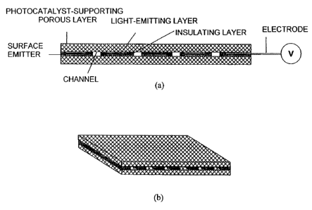
FIG. 1 is a diagram showing an example of a structure of the surface
light-emitting device of the present invention, wherein (a) is a side view and
(b) is a perspective view;
FIG. 2 is a diagram showing another structural example of the surface
light-emitting device of the present invention;
FIG. 3 is a diagram showing an example of the structure of the
inorganic EL device used in the present invention;
FIG. 4 is a diagram showing another structural example of the inorganic
EL device used in the present invention;
FIG. 5 is a diagram showing another structural example of the surface
light-emitting device of the present invention;
FIG. 6 is a diagram showing a structural example of the optically
CA 02570352 2006-12-14
13
assisted ceramic filter of the present invention;
FIG. 7 is a diagram showing the steps of manufacturing the surface
light-emitting device in the embodiments;
FIG. 8 is an explanatory diagram of a method for evaluating the surface
light-emitting device in the embodiments; and
FIG. 9 is an explanatory diagram of a method for evaluating a surface
light-emitting device in a comparative example.
Description of the Preferred Embodiments
[0026]
One essential structure of the surface light-emitting device of the
present invention has a surface emitter having a function for emitting visible
light or ultraviolet light, and a porous layer having a photocatalyst formed
on
the top surface and/or the bottom surface, wherein multiple through-holes as
channels for a fluid are formed in a direction perpendicular to the surface of
the surface emitter. A light-emitting sheet known as an electroluminescence
(EL) sheet is preferably used as the surface emitter having a function for
emitting visible light or ultraviolet light.
[0027]
An example of the specific structure (a first structure) of the surface
light-emitting device of the present invention is shown in FIG. 1. FIG. 1(a)
is a
side view, and FIG. 1(b) is a perspective view.
The surface light-emitting device in FIG. 1 is provided with porous
layers that contain a photocatalyst and are formed on the top and bottom
CA 02570352 2006-12-14
14
surfaces of a surface emitter. In the emitter, multiple rectangular light-
emitting layers are aligned at fixed gap intervals. A treated fluid flows in
through the surface of one porous layer, passes through the gaps in the
surface
emitter, and escapes through the porous layer on the opposite side. The
visible
light or ultraviolet light emitted from the surface emitter is incident
perpendicular to the surfaces of the porous layers on the top and bottom
surfaces of the surface emitter, and is repeatedly reflected in the porous
layers.
Therefore, the light can expand uniformly throughout the entire porous layers,
and the photocatalyst can be excited. The fluid that has passed through the
porous layer on one surface then passes through the gaps in the surface
emitter, and is finally ejected as a clarified fluid through the porous layer
on
the other surface. Fluid permeability increases with an increase in the
surface
area occupied by the gaps in the surface emitter in relation to the surface
area
of the entire top and bottom surfaces of the surface emitter (referred to
herein
as the channel surface area ratio), but [an increase in the surface area of
the
gaps causes] the surface area of the light-emitting portion to decrease and
the
porous structure containing the photocatalyst to not be uniformly exposed to
light; i.e., brightness to be reduced. Generally, the surface area ratio of
the
channels is preferably 30 to 70% of the entire surface area.
[0028]
The surface emitter preferably has no electrode portion and is
electrically insulated from the exterior, as shown in FIG. 1. This results in
a
device that can be used with all kinds of liquids having high electrical
CA 02570352 2006-12-14
conductivity.
A cross section provided with through-holes is also electrically insulated
at this time. One example of the method for sealing the cross section is a
method of temporarily creating an EL sheet provided with through-holes,
5 pouring a liquid resin into the through-holes, drying the resin, and forming
through-holes again in the resin while maintaining electrical insulation.
The surface light-emitting device of the present invention can be
insulated without incurring extra costs because fluid does not pass through
the
light-emitting layer (this is ensured by forming through-holes as channels for
10 the fluid). Furthermore, forming through-holes has the advantage of
allowing
the heat produced during light emission to be quickly discharged via the
through-holes.
[00291
In a second structure of the surface light-emitting device of the present
15 invention, the light-emitting layers are disposed in a lattice pattern, as
shown
in FIG. 2.
In the case of rectangular light-emitting layers, groups of lead wires for
applying voltage must be formed for each of the multiple light-emitting
layers,
but a lattice pattern has the effect of reducing costs because only one group
of
lead wires is needed. A lattice structure is preferred because light is more
uniformly conducted into the porous structure. In this case, the size of the
lattice acting as the channels is preferably 5 mm or less. The channels are
not
limited to this shape and may also be square or circular.
CA 02570352 2006-12-14
16
Also commercially available are EL sheets that have multiple circular
holes formed in advance and that are intended as displays or backlights, and
these sheets may therefore also be used.
[0030]
In the present invention, light emitted from the light-emitting layer can
be concentrated in the channels by controIling the structure of the surface
emitter.
The top and bottom surfaces (the surfaces provided with porous layers)
of the light-emitting layers may be enclosed by metal materials or other
members that reflect but do not transmit visible light or ultraviolet light,
in
which case the light from the light-emitting layers is repeatedly reflected by
and trapped within these members. The light is not discharged to the top and
bottom surfaces but is concentrated in the channels via the cross section of
the
light-emitting layers (the surfaces adjacent to the channels), and the light
is
then discharged from the channels to the exterior. Specifically, with this
type
of structure, the device can be designed so that only the channels emit light.
This type of structure can be easily obtained by selecting a metal material
that
reflects but does not transmit visible light or ultraviolet light, and using
the
material for the electrodes of the organic EL device used as the surface
emitter,
for example.
[0031]
It is apparent that in a device in which porous layers having a
photocatalyst are disposed on the top and bottom of the surface emitter, the
CA 02570352 2006-12-14
17
portions of the porous layers directly above the channels are primarily the
areas that allow the passage of fluid. Concentrating light in these portions
makes it possible to attain the most efficient photocatalytic performance. In
this type of light-condensing structure, a porous structure having a
photocatalyst is embedded not only in the top and bottom of the surface
emitter, but also in the portions of the channels formed, whereby an advantage
is obtained of preventing light loss because the light-emitting source and the
photocatalyst are at a distance of closest approach. With this type of
structure,
the size of the lattice serving as the channels does not need to be 5 mm or
less.
This is because light is concentrated in the channels.
[0032]
With this type of structure, the photocatalyst that is in direct contact
with the cross section of the light-emitting layer of the channels is directly
irradiated with visible light or ultraviolet light that does not pass through
an
intervening space. The photocatalyst has the following problem. Specifically,
when the photocatalyst is placed in a highly contaminated substance, the
contaminants adhere strongly to the surface of the photocatalyst, and the
light
from the external light source does not reach the photocatalyst, impairing the
photocatalytic function. In the surface light-emitting device of the present
invention, a porous structure containing a photocatalyst is loaded into the
channels. The above problem can therefore be resolved because visible light or
ultraviolet light is continuously directed without passing through an
intervening space onto the photocatalyst in direct contact with the cross
CA 02570352 2006-12-14
18
section of the light-emitting layer of the channels.
The porous structures that have a photocatalyst and are packed into the
channels may be porous structures that have a photocatalyst supported
thereon, or porous structures having a photocatalyst packed in the form of a
lattice.
[0033]
Using ultraviolet light that has a wavelength in the vicinity of 254 nm
allows the filtering device to be made to function as a filter having a
sterilizing
effect similar to that of a regular mercury lamp, even without a
photocatalyst.
[0034]
The first electroluminescent structure used in the present invention is
commonly referred to as a dispersive EL, and the light-emitting layers are
configured so that a phosphor that emits visible light or ultraviolet light is
dispersed within a dielectric material.
The second structure is referred to as a thin-film EL and is a structure
in which thin-film light-emitting layers that are 1 fcm or less in thickness
are
enclosed by insulating layers, and the light-emitting layers are composed of
only a phosphor and do not contain a resin.
A thin-film EL is characterized in emitting very bright light. Therefore,
a large amount of light can be emitted and photocatalyst can be efficiently
excited. However, a thin-film EL has drawbacks in that a large amount of
power is consumed because of a low light-emitting efficiency of 1 lm/W or
less,
and this EL also requires an expensive gas-phase synthesis apparatus. A
CA 02570352 2006-12-14
19
dispersive EL, on the other hand, sometimes has low brightness but a light-
emitting efficiency in excess of 10 lm/W, and also has much lower
manufacturing costs because power consumption is low and a powder
application process is used.
[0035]
An organic EL device or an inorganic EL device can be used as the
surface emitter, but an organic EL device is preferably used due to having
superior ultraviolet light resistance and other such durability
characteristics.
Generally, an inorganic EL device is configured primarily from a light-
emitting layer composed of fluorescent particles of ZnS or the like dispersed
within a dielectric resin, and an insulated layer composed of BaTiO3 or
another such highly dielectric ceramic dispersed in a dielectric resin,
wherein
the light-emitting layer is enclosed by insulating layers, and electrodes are
formed on the insulating layers.
[0036]
A structural example of the inorganic EL device used in the present
invention is shown in FIG. 3. In FIG. 3(a), an insulating layer is formed only
on the bottom surface of the light-emitting layer, and in FIG. 3(b),
insulating
layers are formed on both the top and bottom surfaces of the light-emitting
layer. In the present invention, both the front and back surface electrodes
can
be formed from a transparent electroconductive film. Specifically, the front
and back surface electrodes are both formed from a transparent
electroconductive film in cases in which porous layers having a photocatalyst
CA 02570352 2006-12-14
that emits light due to ultraviolet light are placed on the top and bottom
surfaces of the surface emitter. A resin base material and a protective layer
resin are translucent with respect to light having the wavelength emitted by
the surface emitter, and these two members also have electrically insulating
5 properties.
The resin has low UV transmissivity if the wavelength of the emitted
light is that of ultraviolet light. Polyethylene (PET) resins, which are
regularly used, have low transmissivity with respect to ultraviolet light
having
a wavelength of 360 nm or less, and it is therefore preferable to use a W
10 transmitting resin in cases in which the wavelength of the emitted light is
less
than 360 nm. One example of a UV transmitting resin is Acrylite, made by
Mitsubishi Rayon Co., Ltd. Since resins tend to degrade more with a reduction
in the wavelength of the emitted light, this approach has an advantage in that
all of the structural members can be made from inorganic materials without
15 the use of a resin.
[0037]
A metal material or the like that reflects and does not transmit visible
light or ultraviolet light may be used as the front and back electrodes
instead
of a transparent electroconductive film (see FIG. 4), in which case light from
20 the light-emitting layers is repeatedly reflected and trapped by the
electrodes.
The light is not discharged to the top and bottom surfaces but is transmitted
by the cross section of the light-emitting layers, is concentrated in the
channels, and is then discharged to the exterior from the channels. In this
CA 02570352 2006-12-14
21
case, the protective layer resin on the front and back surfaces does not need
to
be transmissive with respect to light having the wavelength emitted by the
surface emitter, but the protective layer resin on the cross section must at
least be transmissive and electrically insulated.
[0038]
Any type of phosphor may be used for electroluminescence. The
following phosphors can be used, for example.
A photocatalyst responsive to visible light can be excited in cases in
which the wavelength of the light emitted by the surface emitter peaks at 540
nm or less. In the case of an inorganic EL device, ZnS doped with Cu, Cl, Al,
or the like has high light-emitting efficiency and is therefore preferably
used
as the phosphor capable of emitting light at this wavelength. These phosphors
have peak wavelengths in the vicinity of 450 to 540 nm, emit blue to green
light, and can excite a photocatalyst responsive to visible light, but_ light
having a peak wavelength of 460 nm or less is preferred for the ability of
this
light to excite the photocatalyst more efficiently.
[00391
The general formula is Zna-,)AaS:Cu, D (wherein A is at least one type of
2A group element selected from among Be, Mg, Ca, Sr, and Ba; D is at least
one type of element selected from among 3B group elements or 7B group
elements; and the value of x is 0 < x < 1), and a material that contains a
phosphor having a function for emitting Blue-Cu light can be used. Al, Ga, Cl,
F, and the like are possible examples of D, but Al and Cl are preferred in
terms
CA 02570352 2006-12-14
22
of raw material costs. The value of x is preferably 0.25 <_ x<_ 0.6.
[0040]
The Blue-Cu emitted light is described hereinbelow. For example, in
the phosphor (ZnS: Cu, Cl), doped Cu is generally substituted in place of Zn,
while Cl is substituted in place of S. Since the wavelength of the emitted
light
is in the vicinity of 530 nm, indicating green, the light is referred to as
Green-
Cu light. The Cu may enter the gaps in the ZnS crystal lattice, and the Cu
may be substituted in place of Zn. The resulting emitted light will be Blue-Cu
light with a short wavelength in the vicinity of 460 nm. Using Cu for doping
causes part of the added Cu to remain in the phosphor as highly conductive
Cu2S, and when an AC electric field is applied to an EL device obtained using
this phosphor, EL light is emitted because of the concentration of the
electric
field in the periphery of the conductive CuzS, and for other reasons. The
wavelength of this emitted light depends on the band gap of the semiconductor
that is the source of the phosphor, and the wavelength of the emitted light
decreases with larger band gaps. Consequently, it is possible to use, e.g.,
ZnS:
Cu, Cl, Al (450 to 460 nm), or Zno.a Mgo.2 S=Cu, Cl, Al (410 to 430 nm) can be
used if Blue-Cu light is used.
[0041]
The phosphor is preferably a UV-emitting phosphor, wherein the peak
wavelength of the emitted light is less than 400 nm, or preferably 300 to 375
nm. In this case, it is possible to excite anatase Ti02, which has the highest
photocatalytic performance.
CA 02570352 2006-12-14
ab
23
ZnS doped with Ag, Cl, Al, or the like is ideal as the phosphor that emits
ultraviolet light. A phosphor containing at least one of Cu, Ag, Au, Li, Na,
N,
As, P, and Sb, which forms an acceptor level in a semiconductor; and at least
one of Cl, Al, I, F, and Br, which forms a donor level in the semiconductor,
is
preferred because of the high light-emitting efficiency of these elements. In
particular, this semiconductor may or may not partially contain ZnS as a
primary component, and a Group II-IV compound semiconductor (MgS, CaS,
SrS, BeS, BaS, or the like) as a secondary element.
[0042]
The general formula is Zn(i-.)AxS*Ag, D (wherein A is at least one type of
2A group element selected from among Be, Mg, Ca, Sr, and Ba; D is at least
one type of element selected from among 3B group elements or 7B group
elements; and the value of x is 0< x < 1), and a phosphor having a function
for
emitting Blue-Cu light can be preferably used. Al, Ga, Cl, F, and the Iike are
possible examples of D, but Al and Cl are preferred in terms of raw material
costs. The value of x is preferably 0.25 _< x< 0.6.
[0043]
The light-emitting mechanism of the phosphor is identical to that of
ZnS:Cu, Cl, and is referred to as Blue-Cu emitted light even in cases in which
Ag is doped. For example, ZnS:Ag, Cl, Al (399 nm) or Zno.8 Mgo.2 S~Ag, Cl, Al
(369 nm) can be used. In the case of Ag, Ag2S is formed similar to the case of
Cu, but since electrical conductivity is low, EL light is not emitted because
no
electric field is concentrated. Consequently, in the case of Ag, EL light can
be
CA 02570352 2006-12-14
~-
24
emitted if the resulting phosphor is compounded with a Cu2S phase or another
electroconductive material by means of another method.
[0044]
Another example of an ideal material is ZnF2: Gd, which reflects
ultraviolet light having a strong emission line spectrum of 311 nm. The
brightness of the emitted light is further improved when Pr is doped together
with Gd. Calcium sulfide is also known as a phosphor that emits light
efficiently by electron beam excitation. Examples include CaS: Gd, F (emits
light at 315 nm), CaS: Cu (emits light at 400 nm), and CaS: Ag, K (emits light
at 388 nm). Calcium oxide is also known as a phosphor that efficiently emits
light with electron beams, despite lacking chemical stability in the
atmosphere.
Examples include CaO: F (emits light at 335 nm), CaO: Cu (emits light at 390
nm), and Ca0 : Zn, F (emits light at 324 to 340 nm).
[0045]
In regular electroluminescence elements, the threshold voltage for
emitting light is estimated at about 1 x 10⁴ to 1 x 10⁶ V/cm, but the
threshold
voltage can be reduced by creating a structure in which the light-emitting
particles are covered with a highly dielectric material.
The wavelength of the emitted light is preferably 350 nm or less because
the photocatalyst can then be excited with maximum efficiency at this
wavelength.
[0046)
A resin or a ceramic is used as the dielectric material. The same resin
CA 02570352 2006-12-14
~-
as is found in regular EL devices may be used for a material that emits
visible
light having a wavelength in excess of 360 nm. A Cyanoresin (made by Shin-
Etsu Chemical Co., Ltd.) or the like can be used as a dielectric resin. At
shorter wavelengths, however, it is preferable to use a dielectric ceramic
5 instead of a resin because a dielectric resin may degrade over time.
Examples
of a dielectric ceramic include BaTiOs, SrTiOs, PbTiO3, and other highly
dielectric materials.
[0047]
Either a dielectric ceramic dispersed in a resin, or a dielectric ceramic
10 alone is used as the insulating layer.
[0048]
A photocatalyst responsive to visible light can be excited in cases in
which the light emitted by the surface emitter has a peak wavelength of 540
nm or less. The photocatalyst responsive to visible light is preferably Ti02:
S,
15 Ti02: N, or the like.
An anatase Ti02 photocatalyst, which has the highest photocatalytic
performance, can be excited in cases in which the emitted light has a peak
wavelength of 400 nm or less. It is preferable that the photocatalyst be
primarily crystalline anatase Ti02, but the photocatalyst may also be
20 crystalline rutile or brookite, which is also crystalline.
[0049]
Any material can be used as the porous layer and porous structure as
long as through-holes are formed in the material, but a foamed metal, a
CA 02570352 2006-12-14
r
26
foamed ceramic, a woven resin fabric, or the like is preferred. These
materials
have high porosity and excellent transmissivity. A photocatalyst can be
supported on these materials. A porous structure composed of a highly
refractive material is more preferred in order to uniformly guide light into a
porous structure having a photocatalyst. For example, there are methods for
forming the porous structure from titanium oxide itself, which is highly
refractive. The porous layer and the porous structure preferably have small
pore diameters because light is then repeatedly reflected within the porous
structure. Ideally, the average pore diameter is 500 gm or less. The pore
diameter in the porous structure can be measured with a mercury porosimeter
or the like. The pore diameter has no lower limit in particular, but ideally
the
lower limit is about 0.005 fcm because the permeation resistance of the fluid
increases as the pore diameter decreases.
The photocatalyst is preferably supported on the porous structure by
means of the sol-gel process. This is because the photocatalytic effects
increase with an increase in the specific surface area of the porous
structure.
(0050]
A thin surface light-emitting device can be made by reducing the
thickness of the porous layer.
The surface light-emitting device of the present invention can be used as
a filtering device, and the entire device is preferably made as thin as
possible
in cases in which the filtering device is used as a filter in an air purifier
or a
filter for an air conditioner. Ideally, the thickness of the EL sheet is 1 mm
or
CA 02570352 2006-12-14
27
less, the thickness of the porous layer having a catalytic function is 1 mm or
less, and the entire device (the sum of the EL sheet and the porous structure
for supporting the photocatalyst) is 3 mm or less in thickness.
[0051]
A ceramic filter can be used as the porous layer. FIG. 5 shows a specific
structural example of a case in which a ceramic filter is used as the porous
layer. FIG. 5(a) is a perspective view, and FIG. 5(b) is a cross-sectional
view of
a surface parallel to the direction in which the feed solution flows.
The structure is obtained substantially by stacking a ceramic filter that
primarily cleans fluids by cross-flow filtration, and a surface light-emitting
sheet in which the channels in the ceramic filter are communicated with the
channels in the surface emitter. The surface light-emitting sheet has through-
holes that preferably have the same cross-sectional shape as those in the
ceramic filter. In the structural example in FIG. 5, the photocatalyst is
formed
as a photocatalytic layer on the inner walls of the channels in the ceramic
filter.
In this case, the light emitted from the light-emitting layers can be
concentrated in the channels by controlling the structure of the surface
emitter.
The light directed into the channels expands throughout the channels while
being repeatedly absorbed and reflected by the inner walls of the channels;
i.e.,
by the photocatalytic layer formed on the surface of the filtration layer. The
photocatalyst is excited in a successive manner.
[0052]
CA 02570352 2006-12-14
28
In cases in which an inorganic EL sheet is used as described above, the
method whereby the light emitted from the light-emitting layers of the surface
emitter is concentrated in the channels involves enclosing the top and bottom
surfaces of the light-emitting layers (the surfaces provided with ceramic
filters) with metal material or other such members that reflect and do not
transmit or absorb visible light or ultraviolet light, in which case the light
from the light-emitting layers is repeatedly reflected and trapped by these
members. The light is not discharged to the top and bottom surfaces, but is
instead concentrated in the channels through the cross sections of the light-
emitting layers (the surfaces near the channels). With an inorganic EL device,
the top and bottom electrodes can be easily created by using aluminum, gold,
or another such metal material for the electrodes.
[0053]
In one example of the method for forming the photocatalytic layer, a
liquid containing dispersed titanium oxide particles is filtered with a
ceramic
filter, a sedimentary layer of titanium oxide particles is formed on the
surface
of the filtration layer, and the resulting formation is heated and baked so
that
the particles are moderately sintered together. The titanium oxide may be
similarly filtered by adjusting the viscosity of an alkoxide solution of
titanium
that has formed after baking the titanium oxide, and the titanium oxide may
be baked again. The filtration layer of the ceramic filter may be formed from
titanium oxide.
[0054]
CA 02570352 2006-12-14
29
The photocatalyst may also be supported on a carrier member instead of
the inner walls of the channels. In this case, the surface emitter may, e.g.,
be
an inorganic EL element so that light is not concentrated in the channels but
is emitted to the top and bottom of the surface emitter. The electrodes can
then be formed from a transparent electroconductive thin film of an indium
and tin-based oxide (ITO) or ZnO or the like. The method for supporting the
photocatalyst in this case involves forming a carrier member by immersing the
carrier member in a liquid obtained by adjusting the viscosity of an alkoxide
solution of titanium that has formed after baking the titanium oxide, and
removing the carrier member out of the liquid and baking the carrier member.
[0055]
The surface light-emitting device of the present invention can have a
stacked structure in which surface emitters and porous layers are repeatedly
stacked.
In cases in which the surface light-emitting device of the present
invention is used as a filtering device, relatively large particles, such as
those
suspended in air, for example, are physically collected on the surfaces of the
porous layers having photocatalysts, and smaller particles are decomposed by
the photocatalysts in the process whereby the particles pass through the
porous layers having photocatalysts. Therefore, repeating the stacked
structure of surface emitters and porous layers results in a highly reliable
filter, but also has drawbacks in that permeability is reduced.
[0056]
CA 02570352 2006-12-14
Next, the opticaIly assisted ceramic filter of the present invention wiA
be described.
The optically assisted ceramic filter of the present invention is a ceramic
filter that primarily cleans liquids by cross-flow filtration. The term "cross-
5 flow filtration" refers to a form of filtration in which a feed solution is
circulated while the treated solution is recovered in a direction
perpendicular
to the flow of the feed solution.
FIG. 6 shows a specific example of a first structure of the optically
assisted ceramic filter of the present invention.
10 The structure is essentially composed of a ceramic filter and a surface
light-emitting sheet in which channels are perpendicular to the cross section.
The structure also has a photocatalytic sheet (photocatalytic layer). The
ceramic filter is composed of a filtration layer for performing filtration, an
intermediate layer, and a carrier member. The photocatalytic sheet is aligned
15 with the cross-sectional shape of the ceramic filter, and is wrapped around
the
side surface of the ceramic filter. The term "the cross section of the ceramic
filter" in the present invention refers to the cross section that is
perpendicular
to the flow of the feed solution, and the term "side surface" refers to the
surface
other than the bottom surface on the front of the cylindrical ceramic filter.
20 [0057]
The clarified fluid that has passed through the filtration layer is then
discharged from the side surface of the ceramic filter and caused to
impregnate
the photocatalytic sheet. Light emitted from the surface emitter excites the
CA 02570352 2006-12-14
31
photocatalyst in the photocatalytic sheet to create a photocatalytic effect,
and
organic substances, bacteria, viruses, and other such substances in the
clarified fluid that could not be collected or decomposed by filtration are
decomposed or destroyed.
After being subjected to the decomposition and sterilization treatment,
the fluid is recovered from the interior of the photocatalytic sheet, along
the
inner surface, and from the end of the ceramic filter. In cases in which
multiple through-holes are formed in the surface light-emitting sheet in a
direction perpendicular to the surface of the surface emitter (in a direction
perpendicular to the side surface of the ceramic filter), the fluid that has
undergone decomposition and sterilization treatment can be discharged to the
exterior via these through-holes. The amount of fluid that can be recovered is
therefore greater than in cases in which no through-holes are formed.
Conversely, through-holes must be formed in the surface light-emitting sheet
in cases in which the permeability of the ceramic filter must be increased.
The surface light-emitting device having through-holes acc according to
the present invention can be used as a surface light-emitting device that has
through-holes.
[0058]
The photocatalytic sheet is composed of a photocatalytic powder
supported on the surface of a resin, metal, or ceramic porous structure. The
sheet may be obtained by forming a coating of a photocatalytic film. The side
surface of the ceramic filter may be coated with a photocatalyst. Titanium
CA 02570352 2006-12-14
32
oxide is a common photocatalyst. Therefore, the light emitted by the surface
emitter must have a wavelength that lies within a wavelength band capable of
exciting the photocatalyst. Light having a peak wavelength of 460 nm or less
is preferred in the case of a photocatalyst responsive to visible light.
Photocatalytic performance is sometimes observed if the wavelength exceeds
460 nm, but the performance is reduced. The light preferably has a peak
wavelength of 400 nm or less in the case of anatase titanium oxide, which is a
photocatalyst responsive to ultraviolet light. Photocatalysts responsive to
ultraviolet light generally exhibit better performance in terms of
photocatalytic action.
[0059]
In an optically assisted ceramic filter, the surface emitter must be
flexible and capable of bending because the surface emitter must be wrapped
around the side surface of the ceramic filter. An organic EL sheet, inorganic
EL sheet, or other such sheet is therefore preferred. A dispersive inorganic
EL
sheet is preferred in order to allow low-cost manufacturing of a surface
emitter
in which multiple through-holes are formed perpendicular to the surface of the
surface emitter. The term "dispersive inorganic EL" refers to the concept of
forming light-emitting layers having phosphor dispersed in a dielectric resin
on the surface of a resinous substrate sheet by screen printing, the doctor
blade method, or another such method, and causing light to be emitted by
applying an AC electric field to the electrodes formed on the top and bottom
of
the light-emitting layers. Inorganic EL is also preferred because of its high
CA 02570352 2006-12-14
33
moisture resistance. Although it is difficult for ultraviolet light to be
emitted
with organic EL, organic EL has an advantage with visible light in that a high
degree of brightness is obtained more easily than with inorganic EL.
Inorganic EL has problems with a short service life when used in water
because of its low moisture resistance.
[00601
An organic EL or inorganic EL device can be used as the surface emitter,
but an inorganic EL device having excellent UV resistance and other such
durability characteristics is preferred in the case of ultraviolet light
having a
peak wavelength of 400 nm or less. As described above, the principal
structural elements of an inorganic EL surface emitter are usually light-
emitting layers in which particles of ZnS or another such phosphor are
dispersed in a dielectric resin, and insulating layers wherein BaTiOs or
another such highly dielectric ceramic is dispersed in a dielectric resin.
Electrodes are formed on the insulating layers. The resin easily degrades
when the wavelength of the emitted light is that of ultraviolet light. It is
therefore advantageous in this case to use inorganic materials for all of the
structural components instead of using a resin. However, since the resin often
degrades with ultraviolet light primarily having a wavelength of 350 nm or
less, a res' may be used in cases not involving ultraviolet light in this
wavelength range.
[0061]
The light emitted from the light-emitting layers can be concentrated on
CA 02570352 2006-12-14
34
the side of the photocatalytic sheet by controlling the structure of the
surface
emitter. For example, an inorganic EL device can be provided with a structure
in which light is emitted only inward (towards the light-emitting layers).
This
can be achieved by forming the outward-facing electrodes from aluminum, gold,
or another such metal material.
[0062]
The same phosphor as is used in the surface light-emitting device
described above can be used as the phosphor in the surface emitter.
[0063]
The optically assisted ceramic filter of the present invention primarily
cleans liquids by cross-flow filtration, but gases may also be filtered. The
term
"cross-flow filtration" refers to a form of filtration in which a feed
solution is
circulated while the treated solution is recovered in a direction
perpendicular
to the flow of the feed solution. If the optically assisted ceramic filter of
the
present invention is used, the bacteria or organic matter that could not be
collected by physical filtration can be decomposed or destroyed by the
photocatalytic action. [Embodiments]
[0064]
The present invention is described in further detail hereinbelow by
means of embodiments.
Embodiment (1)
1. Preparation
CA 02570352 2006-12-14
(Protective layer resin)
A transparent resin sheet (trade name: Acrylite S, product #000,
Mitsubishi Rayon Co., Ltd.) 100 x 100 mm in size and 100 fcm in thickness
was prepared. Lattice-shaped holes of various sizes were formed in this sheet
5 in advance at intervals (a pitch) of 4 mm.
(Insulating layer)
BaTiOs: average grain size: 0.2 gm
Resin: made by Shin-Etsu Chemical Co., Ltd. (trade name: Cyanoresin)
(Phosphor)
10 ZnS: Cu, Cl powderaverage grain size: 3 ftm peak wavelength of
emitted light= 533 nm (green)
ZnS: Cu, Cl, Al powder average grain size: 3 ftm peak wavelength of
emitted light: 450 nm (blue)
ZnS: Ag, Cl powderaverage grain size 3 fcm peak wavelength of
15 emitted light: 380 nm (ultraviolet light)
(Porous structure)
An SiC porous structure was used, having a size of 120 x 120 mm, a
thickness of 0.1 mm, and a porosity of 50% with the various average pore
diameters shown in Table 1.
20 (Photocatalyst)
Anatase Ti02 average grain size: 0.03 /cm (commercially available)
Ti02: S average grain size 0.03,um
Thiourea (CH4N2S) powder and Ti(OC3H7)4 were mixed in ethanol, and
CA 02570352 2006-12-14
w
36
were concentrated in a vacuum until a white slurry was formed. The slurry
was baked for 2 hours at 588 C under atmospheric conditions to obtain a
powder. The amount of doped S in relation to oxygen was 2 at%.
[0065]
2. Steps
A surface light-emitting device was manufactured as shown in FIG. 7 by
following the steps hereinbelow.
(1) Formation of electrode 1
The protective layer resin (FIG. 7(a)) was coated by sputtering with
aluminum in a lattice pattern having a line width of 50 Ecm and a thickness of
0.1 fcm, and an electrode lead wire was attached (FIG. 7(b)). The entire
lattice-
patterned sheet was then coated with a 0.1-,um transparent electroconductive
film (ITO) (FIG. 7(c)).
[0066]
(2) Formation of inner insulating layer
The resin (made by Shin-Etsu Chemical Co., Ltd. (trade name:
Cyanoresin)) was dispersed and dissolved in an amount of 25 vol% relative to
cyclohexanone, and a BaTiOa powder was dispersed (25 vol%) to form a slurry.
A coating layer having a thickness of 30 fcm was formed by screen printing on
the electrode (FIG. 7(d)).
(3) Formation of light-emitting layer
A resin (Cyanoresin) was dispersed and dissolved in an amount of 25
vol% relative to cyclohexanone. A slurry was formed by subjecting the
CA 02570352 2006-12-14
37
pulverulent phosphor to a dispersion treatment (25 vol%) in this solution in
an
Ar gas. A coating layer having a thickness of 60 Ecm was formed by screen
printing on the surface of the inner insulating layer (FIG. 7(e)).
[0067]
(4) Formation of electrode 2
The surface of the light-emitting layer was coated with a transparent
electroconductive film in the same manner as the electrode 1, and an electrode
lead wire was attached (FIG. 70.
(5) Sealing
A sheet having the same shape as the protective layer resin used in (1)
was overlaid, and was then thermocompression bonded and completely sealed
(FIG. 7(g)). An epoxy resin was then applied over the cross section of the
through-holes.
[0068]
(6) Supporting the photocatalyst
A solution was prepared by dispersing photocatalytic particles in alcohol,
an SiC porous structure was immersed therein, and the structure was lifted
out at a speed of 0.003 m/s. The resulting structure was then heated for 0.5
hours at 300 C under atmospheric conditions, and the walls of the pores in the
SiC porous structure were coated with photocatalytic particles. This process
was repeated ten times.
(7) Stacking
An SiC porous structure for supporting a photocatalyst was disposed on
CA 02570352 2006-12-14
38
the top and bottom surfaces of a surface light-emitting sheet, and the ends
were screwed shut, resulting in a filtering device.
[0069]
3. Evaluation
(1) Photocatalytic reaction experiment
2,3',4,4',5-Pe-CB, a type of dioxin, was dissolved in water to prepare 3.0
L of a solution having a concentration of 55 pg/L. 5% of india ink solution
was
added in advance in order to intentionally color the water, so that the liquid
was made to have high turbidity. The resulting liquid and the filtering device
prepared as described above were placed in the apparatus shown in FIG. 8.
The resulting liquid was circulated at a flow rate of 0.3 L/min, while AC
electric fields having the voltages and frequencies shown in Table 1 were
applied between the electrodes. The time elapsed until the dioxin was
completely decomposed was measured, with a maximum time of 100 hours.
[0070]
As a comparative example, only SiC porous structures for supporting
the photocatalysts shown in Table 1 were placed in the apparatus shown in
FIG. 9, and the same photocatalytic reaction experiment as in the embodiment
was conducted while a UV LED lamp having an emitted light wavelength of
360 nm and an output of 5 mW was illuminated from a distance of 50 mm.
The results are shown in Table 1.
[00711
[Table 11
Embodiment (1)
Average pore Porosity Inner Light- Time of
diameter o of SiC ~~ice Channel insulating emitting Frequ Wavelength
hole Pitch surface Type o Voltage Type o decompo
SiC porous porous layer layer ency of emitted
size (mm) area phosphor (v) photocatalyst sition
structure structure (mm) ratio ("/o) thickness thickness (Hz) light (nm) (hr)
(%)
0.1 50 5 4 56 30 60 ZnS*A , Cl 120 550 380 anatase Ti02 6.3
1 50 1.5 4 27 30 60 ZnS*A , Cl 120 550 380 anatase Ti02 10.2 N
1 50 2 4 33 30 60 ZnS=A , Cl 120 550 380 anatase Ti02 8.6 Ln
1 50 5 4 56 30 60 ZnS*A , Cl 120 550 380 anatase Ti02 8.5 0
1 50 7.5 4 65 30 60 ZnS*A Cl 120 550 380 anatase Ti02 10.6 ~
1 50 10 4 71 30 60 ZnS~A , Cl 120 550 380 anatase Ti02 12.2 0
50 5 4 56 30 60 ZnS*A , Cl 120 550 380 anatase Ti02 23 0'
400 50 5 4 56 30 60 ZnS~A Cl 120 550 380 anatase Ti02 77 N
600 50 5 4 56 30 60 ZnS*A , Cl 120 550 380 anatase TiOz 99.5 ~
0.1 50 5 4 56 30 60 ZnS*A , Cl 120 5000 380 anatase T102 3.6
1 50 5 4 56 30 60 ZnS~A Cl 120 5000 380 anatase TiOz 6.4
10 50 5 4 56 30 60 ZnS~A , Cl 120 5000 380 anatase TiOz 18
1 50 5 4 56 30 60 Ci ~ u' 120 550 450 Ti02:S 44
1 50 5 4 56 30 60 ZnS:Cu, Cl 120 550 530 Ti02:S 88
* 1 50 5 4 56 LED 360 anatase Ti02 100<
* Indicates a comparative example
5
CA 02570352 2006-12-14
[0072]
The filtering device obtained using the surface light-emitting device of
the present invention had a shorter decomposition time than a filter having an
external light source. The reason for this is believed to be that only the
polar
5 surfaces of the Ti02 porous structure were able to be excited in a$lter
having
an external light source, because the emitted light is easily absorbed in a
liquid having high turbidity.
The filtering device obtained using the surface light-emitting device of
the present invention has a shorter decomposition time because the catalytic
10 function acts uniformly over the entire Ti02 porous structure layer while
the
emitted light is repeatedly scattered within this porous structure layer.
[0073]
Embodiment (2)
1. Preparation
15 (Protective layer resin)
A transparent resin sheet (trade name: Acrylite S, product #000,
Mitsubishi Rayon Co., Ltd.) 100 x 100 mm in size and 100 am in thickness
was prepared. Lattice-shaped holes having a size of 1 mm were formed on one
side of this sheet in advance at intervals of 1 mm.
20 (Insulating layer)
BaTi03: average grain size: 0.2 gm
Resin: made by Shin-Etsu Chemical Co., Ltd. (trade name: Cyanoresin)
(Phosphor)
CA 02570352 2006-12-14
41
ZnS: Ag, Cl powder; average grain size: 3 fcm; peak wavelength of
emitted light: 380 nm (ultraviolet light)
ZnS-20 mol% MgS: Ag, Cl powder; average grain size: 3 fcm; peak
wavelength of emitted light: 366 nm (ultraviolet light)
ZnF2: Gd, Pr, Cu powder; average grain size: 3 fcm- peak wavelength of
emitted light: 311 nm (ultraviolet light)
(Photocatalyst)
Anatase Ti02; average grain size: 0.03 fcm (commercially available)
[0074]
2. Steps
A surface light-emitting device was manufactured according to
Embodiment (1) by following the steps hereinbelow.
(1) Formation of electrode 1
The protective layer resin was coated with 0.1 pm of aluminum by
sputtering, and an electrode lead wire was attached.
[0075]
(2) Formation of inner insulating layer
The resin (made by Shin-Etsu Chemical Co., Ltd. (trade name:
Cyanoresin)) was dispersed and dissolved in an amount of 25 vol% relative to
cyclohexanone, and a BaTiOs powder was dispersed (25 vol%) to form a slurry.
A coating layer having a thickness of 30 fcm was formed by screen printing on
the electrode.
(3) Formation of light-emitting layer
CA 02570352 2006-12-14
42
A resin (Cyanoresin) was dispersed and dissolved in an amount of 25
vol% relative to cyclohexanone. A slurry was formed by subjecting the
pulverulent phosphor to a dispersion treatment (25 vol%) in this solution in
an
Ar gas. A coating layer having a thickness of 60 fcm was formed by screen
printing on the surface of the inner insulating layer.
[0076]
(4) Formation of electrode 2
The surface of the light-emitting layer was coated with aluminum in the
same manner as the electrode 1, and an electrode lead wire was attached.
(5) Sealing
A sheet having the same shape as the protective layer resin used in (1)
was overlaid, and was then thermocompression bonded and completely sealed.
(6) Supporting the photocatalyst
Photocatalytic particles were molded into a diameter of 1 mm and a
thickness of 300 um by dry pressing, and a porous structure having a porosity
of 65% was formed. The holes (channels) were filled with a resin adhesive, and
the structure was solidified.
[0077]
3. Evaluation
(1) Photocatalytic reaction experiment
Formaldehyde was dispersed in the air to prepare 3.0 L of polluted air
having a concentration of 0.5 ppm. The resulting polluted air and the
filtering
device manufactured as described above were placed in the same apparatus as
CA 02570352 2006-12-14
43
in Embodiment (1).
The resulting polluted air was circulated at a flow rate of 0.3 L/min,
while AC electric fields having the voltages and frequencies shown in Table 2
were applied between the electrodes. The time elapsed until the formaldehyde
concentration reached zero was measured.
[0078]
As a comparative example, photocatalytic particles were molded into a
diameter of 100 mm and a thickness of 300 fcm by dry pressing, and a porous
structure having a porosity of 65% was formed. A photocatalytic reaction
experiment was conducted while this photocatalytic sheet was irradiated from
above and below by a UV LED lamp having an output of 5 mW. The
wavelength of emitted light was 360 nm. The lamp was placed at a distance of
50 mm.
The results are shown in Table 2.
[00791
[Table 2]
Embodiment (2)
Inner Light- Lattice Channel
insulating emitting Wavelength Time for
hole Pitch surface Frequency Type of layer layer Type of phosphor Voltage (v)
of emitted decomposition
thickness thickness size (mxn) area (HZ) light (nm) photocatalyst Gmlx)
(MM) ratio (%)
30 60 1 1 50 ZnS~ , Cl 120 550 380 anatase Ti02 18
30 60 1 1 50 AnS-20M S: Ag, Cl 120 550 366 anatase TiOz 10
30 60 1 1 50 ZnF2:Gd, Pr, Cu 120 4000 311 anatase'IiOa 30
0
N
* LED 360 anatase Ti02 77 o
w
* Indicates a comparative example N
N
0
0
0)
H
N
H
CA 02570352 2006-12-14
[0080]
In the filtering device obtained using the surface light-emitting device of
the present invention, it was visually confirmed that only the holes emitted
light before the photocatalyst was introduced.
5 The filtering device of the present invention had a shorter
decomposition time than when an LED was used. The reason for this is
believed to be that light from an external light source is easily reflected by
the
photocatalytic sheet and cannot efficiently excite the photocatalyst, and also
that the light attenuates due to the distance of the light source. In a
filtering
10 device obtained using the surface light-emitting device of the present
invention,
light is concentrated in the holes, the light source is in contact with the
filled
photocatalyst, and there is little light attenuation because the light source
and
the photocatalyst are extremely close to each other, whereby the filter is
believed to be endowed with high decomposition efficiency.
15 Thus, the filtering device of the present invention does not need an
external light source, and the filter is therefore thin and requires little
space.
[0081]
Embodiment (3)
The filtering device was created in the same manner as in Embodiment
20 (2) except that the channels were filled with the photocatalyst, and the
following porous layer was overlaid.
(Porous resin sheet)
A porous film (porosity 95%) made from a fluorine resin and having a
CA 02570352 2006-12-14
46
size of 100 x 100 mm and a thickness of 100 fcm was prepared.
(Photocatalyst)
Anatase Ti02; average grain size: 0.03 fcm (commercially available)
A suspension was prepared by dispersing a photocatalyst in ethanol at a
concentration of 30 vol%, the porous resin sheet was immersed in this
solution,
and the sheet was then withdrawn and dried at room temperature. These
steps were repeated ten times, and the resulting photocatalyst-supporting
sheet was stacked on the top and bottom of the perforated EL sheet.
[0082]
(Photocatalytic reaction experiment)
Toluene was dispersed in the air to prepare 3.0 L of polluted air having
a concentration of 500 ppm. The resulting polluted air and the filtering
device
manufactured as described above were placed in the same apparatus as shown
in FIG. 8.
The resulting polluted air was circulated at a flow rate of 0.3 L/min,
while AC electric fields having the voltages and frequencies shown in Table 3
were applied between the electrodes. The time elapsed until the toluene
concentration reached zero was measured.
[0083]
As a comparative example, a photocatalytic reaction experiment was
conducted while two stacked sheets supporting the same photocatalyst were
irradiated from above and below by a UV LED lamp having an output of 5 mW.
The wavelength of emitted light was 360 nm. The lamp was placed at a
CA 02570352 2006-12-14
.r.
47
distance of 50 mm.
The results are shown in Table 3.
M
[0084]
[Table 3]
Embodiment (3)
Inner Light- Channel
insulatin emitting Lattice Wavelength Time for
Pitch surface Frequency Type of
g layer layer hole size Type of phosphor Voltage (v) of emitted decomposition
thickness thickness (mnm) ~~ area ~z) light (nm) photocatalyst (min)
ratio (%)
30 60 1 1 50 ZnS: Ag,C1 120 1000 380 anatase Ti02 33
~
30 60 1 1 50 ZnS~ OMgS= 120 1000 366 anatase Ti02 25 0
Ag, 30 60 1 1 50 ZnF2:Gd, Pr, Cu 120 5000 311 anatase T102 41 Ln
0
po ~
* LED 360 anatase Ti02 50 N
N
* Indicates a comparative example 0
0)
~
N
F-'
iP
CA 02570352 2006-12-14
49
[0085]
The filtering device of the present invention had a shorter
decomposition time than when an LED was used. Even light from an external
light source could easily reach the interior of the photocatalytic sheet in
cases
in which the photocatalytic sheet supporting the photocatalyst had high
porosity, as was the case in the present embodiment. Therefore, although the
difference in decomposition performance was not as great as in Embodiment
(1) or (2), the filtering device obtained using the surface light-emitting
device
of the present invention was confirmed to be superior. The reason for this is
believed to be that the photocatalytic sheet is not uniformly irradiated
because
the light emission of the LED light source is directional.
Thus, the filtering device of the present invention does not need an
external light source, and the filter is therefore thin and requires little
space.
[00861
Embodiment (4)
(1) Ceramic filter
A multilayered (three-layered) filter, made by NGK Insulators, Ltd., had
thirty-seven holes that each had a diameter of 3 mm and was formed in a cross
section 30 mm in diameter. The length was 500 mm and the porosity was 35%.
This filter successfully separated 100 percent of particles that were 0.2 gm
in
size. This ceramic filter was cut into lengths of 30 mm to prepare sixteen
pieces.
(2) Photocatalytic coating
CA 02570352 2006-12-14
The ceramic filter was used to filer a sol (made by Sumitomo Chemical
Co., Ltd.) containing a titanium oxide powder responsive to visible light
(average grain size 60 nm), or to filter a feed solution containing anatase
titanium oxide powder (average grain size 60 nm, made by Tayca Corporation);
a titanium oxide layer 10 fcm in thickness was formed on the inner walls of
the
channels; and the layer was baked for one hour at 500 C under atmospheric
conditions and solidified.
(3) Surface emitter
1. Resin sheet
A sheet (made by Mitsubishi Rayon Co., Ltd., #000) that transmitted
ultraviolet light and had a size of 95 x 500 mm and a thickness of 100 fmn was
prepared.
2. Insulating layer
BaTiOs= average grain size: 0.2 fcm
Resin: made by Shin-Etsu Chemical Co., Ltd. (trade name: Cyanoresin)
[0087]
3. Phosphor
ZnS: Cu, Cl powder average grain size: 3 fcm
ZnS: Cu, Cl, Al powder average grain size: 3 fcm
ZnS-20 mol% MgS: Cu, Cl, Al powder average grain size: 3 pm
ZnS-40 mol% MgS: Cu, Cl, Al powder average grain size: 3pm
ZnS: Ag, Cl powder average grain size: 3,cm
ZnS-20 mol% MgS: Ag, Cl powder average grain size: 3,um
CA 02570352 2006-12-14
51
In the cases of ZnS: Ag, Cl, and ZnS-20 mol% MgS= Ag, Cl, the phosphor
surfaces were coated with Cu2S.
4. Formation of rear surface electrode
A resin sheet was coated with a 0.4-fcm Al electrode film by sputtering,
and an electrode lead wire was attached to the Al film.
[0088]
5. Formation of insulating layer
A resin was dispersed and dissolved in an amount of 25 vol% relative to
cyclohexanone, and a BaTiOs powder was dispersed (25 vol%) to form a slurry.
A coating layer having a thickness of 30 pm was formed by screen printing on
the ITO electrode.
6. Formation of light-emitting layer
A resin was dispersed and dissolved in an amount of 25 vol% relative to
cyclohexanone. A slurry was formed by subjecting the pulverulent phosphor to
a dispersion treatment (25 vol%) in this solution in an Ar gas. A coating
layer
having a thickness of 60 fcm was formed by screen printing on the surface of
the insulating layer.
[008s]
7. Formation of front surface electrode and sealing
A resin sheet was coated with a 0.2-,um Al electrode film by sputtering,
and an electrode lead wire was attached to the Al film.
A light-emitting layer was laid over the Al electrode side of this sheet,
and the resulting stack was thermocompression bonded at 120 C and sealed to
CA 02570352 2006-12-14
52
form a surface light-emitting sheet.
8. Hole formation
Seventeen EL sheets manufactured in this manner were prepared by
punching the sheets into the same size and structure as the cross section of
the
ceramic filter in (1).
[0090]
(4) Assembly
Perforated EL sheets were stacked alternately on the cross section of
the 30 mm long ceramic filter, forming a stacked ceramic filter about 480 mm
in length.
[0091]
(5) Filtration experiment
1. Suspension preparation
mg of aluminum particles with an average grain size of 0.5 ,um were
dispersed in 10 L of water, trichloroethylene was added, and the solution was
adjusted until the concentration reached 1 ppm.
2. Filtration
A filter was placed in a cross-flow filtration apparatus, and an AC
electric field of 500 V and 5 kHz was applied between the electrodes of the EL
sheet while filtration was performed at a transmembrane pressure difference
of 1 kg/cm2. The experiment was also conducted on a ceramic f lter with no
electric field.
3. Evaluation
CA 02570352 2006-12-14
53
The aluminum particle concentration after filtration was measured with
an absorptiometer. The trichloroethylene (TCE) concentration after filtration
was analyzed with a gas chromatograph.
The results are shown in Table 4.
[0092]
[Table 4]
Embodiment (4)
EL Peak wavelength Voltage Frequency Brightness Permeability Aluminum TCE
No sheet Phosphor of emitted light (V) (Hz) (cdjm2) Photocatalyst (Umin)
removal ratio concentration
Gnm) W (ppm)
* 1 none 500 5000 none 0.4 99< 1.00
2 ZnS: Cu, Cl 516 500 5000 350 responsive to 0.22 99< 0.80
visible li ht ~
ZnS: Cu Cl responsive to 0
3 Al ' ' 455 500 5000 200 visible li ht 0.22 99< 0.40 Ln
4 ZnS-20MgS: 430 500 5000 122 responsive to 0.22 99< 0.53 cn W
Cu, Cl, Al visible li ht N
ZnS-40MgS: responsive to 0
Cu Cl, Al 408 500 5000 88 visible li ht 0.22 99< 0.58 0
0)
6 ZnS: Ag, Cl 399 500 5000 55 responsive to 0 22 99< 0.52 N
visible li ht
~
ZnS-20MgS: responsive to
0.22 99< 0.61
7 Ag, Cl 369 500 5000 23 visible light
8 ~: Cu, Cl, 455 500 5000 200 anatase 0.22 99< 0.81
9 ZnS : Ag, Cl 399 500 5000 55 anatase 0.22 99< 0.00
A S-C20MgS: 369 500 5000 23 anatase 0.22 99< 0.00
* Indicates a comparative example
CA 02570352 2006-12-14
[0093]
As a result of stacking the ceramic filter and the surface emitter and
solidifying the photocatalyst on the inner walls of the channels in the
ceramic
filter, the photocatalyst was provided with a greater surface area than the
5 ceramic filter having a wrapped photocatalytic sheet and surface emitter,
and
the decomposition efficiency of the TCE was therefore greater.
[0094]
Embodiment (5)
(1) Ceramic filter
10 A multilayered (three-layered) filter, made by NGK Insulators, Ltd., had
thirty-seven holes that each had a diameter of 3 mm and was formed in a cross
section 30 mm in diameter. The length was 500 mm and the porosity was 35%.
This filter successfully separated 100 percent of particles that were 0.2 pm
in
size.
15 [0095]
(2) Photocatalytic sheet
A polyethylene sheet measuring 95 mm x 500 mm and having a
porosity of 90% was prepared. This sheet was immersed in a sol (made by
Sumitomo Chemical Co., Ltd.) containing a titanium oxide powder responsive
20 to visible light (average grain size 60 nm), or a sol containing anatase
titanium
oxide powder (average grain size 60 nm, made by Tayca Corporation). The
sheet was then taken out and dried at room temperature for 24 hours, and the
surface of the resin was coated with a photocatalyst.
CA 02570352 2006-12-14
56
[0096]
(3) Surface emitter
1. Resin sheet
A resin sheet (made by Mitsubishi Rayon Co., Ltd., #000) that
transmitted ultraviolet light and had a size of 95 x 500 mm and a thickness of
100,um was prepared.
2. Insulating layer
BaTiOa: average grain size: 0.2 pm
Resin: made by Shin-Etsu Chemical Co., Ltd. (trade name: Cyanoresin)
[0097]
3. Phosphor
ZnS: Cu, Cl powder average grain size: 3 ftm
ZnS: Cu, Cl, Al powder average grain size: 3 fcm
ZnS-20 mol% MgS: Cu, Cl, Al powder average grain size: 3,um
ZnS-40 mol% MgS: Cu, Cl, Al powder average grain size: 3 fcm
ZnS= Ag, Cl powder average grain size: 3 pm
ZnS-20 mol% MgS: Ag, Cl powder average grain size: 3 fcm
In the cases of ZnS: Ag, Cl, and ZnS-20 mol% MgS: Ag, Cl, the phosphor
surfaces were coated with Cu2S.
4. Formation of rear surface electrode
A resin sheet was coated with a 0.4-,um Al electrode film by sputtering,.
and an electrode lead wire was attached to the Al film.
[0098]
CA 02570352 2006-12-14
57
5. Formation of insulating layer
A resin was dispersed and dissolved in an amount of 25 vol% relative to
cyclohexanone, and a BaTiOs powder was dispersed (25 vol%) to form a slurry.
A coating layer having a thickness of 30 fcm was formed by screen printing on
the ITO electrode.
6. Formation of light-emitting layer
A resin was dispersed and dissolved in an amount of 25 vol% relative to
cyclohexanone. A slurry was formed by subjecting the pulverulent phosphor to
a dispersion treatment (25 vol%) in this solution in an Ar gas. A coating
layer
having a thickness of 60 gm was formed by screen printing on the surface of
the insulating layer.
[0099]
7. Formation of front surface electrode and sealing
A resin sheet was coated with a 0.2-fcm Al electrode film by sputtering,
and an electrode lead wire was attached to the Al film.
A light-emitting layer was laid over the ITO electrode side of this sheet,
and the resulting stack was thermocompression bonded at 120 C and sealed to
form a surface light-emitting sheet.
8. Hole formation
Holes measuring 3 mm in diameter were formed at a pitch of 3 mm in
the surface of this sheet using a punching machine. The cross section of these
holes was then sealed with an adhesive.
[0100]
CA 02570352 2006-12-14
58
(4) Assembly
A photocatalytic sheet was wrapped around the side surface of the
ceramic filter, and a surface emitter was wrapped over the photocatalytic
sheet.
(5) Filtration experiment
1. Suspension preparation
mg of aluminum particles with an average grain size of 0.5 fcm were
dispersed in 10 L of water, trichloroethylene was added, and the solution was
adjusted until the concentration reached 1 ppm.
2. Filtration
10 A filter was placed in a cross-flow filtration apparatus, and an AC
electric field of 500 V and 5 kHz was applied between the electrodes of the EL
sheet while filtration was performed at a transmembrane pressure difference
of 1 kg/cm2. The experiment was also conducted on a ceramic filter with no
electric field.
3. Evaluation
The aluminum particle concentration after filtration was measured with
an absorptiometer. The trichloroethylene (TCE) concentration after filtration
was analyzed with a gas chromatograph.
The results are shown in Table 5.
[oioll
[Table 51
Embodiment (5)
EL Peak wavelength Voltage Frequency Brightness rrmabffit3T ~uminum TCE
No sheet Phosphor of light (~ (Hz) (cd/m2) Photocatalyst ~~ removal
concentration
ratio (%) (ppm)
* 1 none none 0.40 99< 1.00
0.38 99< 0.90
2 Zn5: Cu, Cl 516 500 5000 350 responsive to vi sible light
3 ZnS: Cu, Cl, Al 455 500 5000 200 responsive to 0.38 99< 0.50 N
visible li ht
ZnS-20MgS: responsive to 0
4 Cu, Cl, Al 430 500 5000 122 visible li ht 0.38 99< 0.62 ~
ZnS-40MgS: responsive to 0
Cu, Cl, Al 408 500 5000 88 visible li ht 0.38 99< 0.65
6 ZnS: Ag, Cl 399 500 5000 55 responsive to 0.38 99< 0.60 ~
visible li ht
7 ZnS-20MgS: 369 500 5000 23 responsive to 0.38 99< 0.70
Ag, Cl visible light
8 ZnS: Cu, Cl 516 500 5000 350 anatase 0.38 99< 0.98
9 ZnS: Cu, Cl, Al 455 500 5000 200 anatase 0.38 99< 0.90
ZnS: Ag, Cl 399 500 5000 55 anatase 0.38 99< 0.20_____l
11 ZAnSC 0MgS: 369 500 5000 23 anatase 0.38 99< 0.00
* Indicates a comparative example
CA 02570352 2006-12-14
.=
[0102]
As a result of wrapping the photocatalytic sheet and the surface emitter,
not only was a filtration function achieved, but TCE could also be decomposed.
When a photocatalyst responsive to visible light was used, decomposition
5 progressed as the wavelength of emitted light grew shorter. The reason for
this is believed to be that the energy of the light was greater. Decomposition
performance was not as high when a photocatalyst responsive to visible light
was combined with an EL sheet that emitted ultraviolet light having a peak
wavelength of 400 nm or less. The reason for this is believed to be that the
10 light emitted by the EL sheet had lower intensity (the sum of the intensity
of
visible light and the intensity of ultraviolet light).
[0103]
High decomposition performance was exhibited with a UV-emitting EL
sheet in cases in which an anatase photocatalyst was used. The reason for this
15 is believed to be that the anatase photocatalyst performance was greater
than
that of a photocatalyst responsive to visible light, and relatively high
photocatalytic performance was therefore achieved even when the intensity of
the light emitted by the EL sheet (the sum of the intensity of visible light
and
the intensity of ultraviolet light) was low.
20 [Industrial Applicability]
[0104]
The surface light-emitting device of the present invention can be used as
a filtering device. In this case, substances that are larger than the pores in
a
CA 02570352 2006-12-14
61
porous structure having a catalytic function are collected from among
particles
suspended in a fluid. Since the surface light-emitting device of the present
invention can be made to have an extremely thin structure, the device has
various applications and yields significant effects when used as a filter for
air
purification or the like. For example, an air conditioner or the like can be
provided with an air purifying function when the device is placed in the air
intake opening of the air conditioner.
The surface light-emitting device of the present invention is
characterized in having an efficient heat radiation function because of the
presence of through-holes, for which reason the surface emitter does not
easily
deteriorate from heat even when high voltages and high frequencies are
applied to emit light.
The surface light-emitting device of the present invention can be used in
display applications while transmitting air or other gases. The display would
have a long service life because heat generation can be prevented in this case
as well.
[0105]
The surface light-emitting device of the present invention can be applied
to various fields, including the decomposition and removal of contaminants in
the atmosphere, such as NOx, SOx, CO gas, diesel particulates, pollen, dust,
and ticks; the decomposition and removal of organic compounds contained in
sewage; the sterilization of common bacteria and viruses; the decomposition of
harmful gases produced by chemical plants; the decomposition of odorous
CA 02570352 2006-12-14
..
62
components; and the like. As a manufactured product, the present invention
can be developed as all kinds of filters in the aforementioned fields, and can
be
applied to air purification, sewage filtration, various types of water
purifiers,
insect repellent, and the like.
The present invention can also be used in EL displays, light sources for
backlights in portable phones, light sources for fixing toner used in digital
photo printers for digital cameras, light sources for curing UV cured resins,
and sterilizing light sources in medical photocatalyst-coated catheters.
When combined with an afterglow phosphor that emits visible light, the
present invention can be used as a display or filter that emits light by means
of AC electric fields during daylight hours, and continues to emit light
without
a power source during nighttime hours.
The present invention can also be used as a sheet-like insect-attracting
panel by taking advantage of the fact that insects are drawn to ultraviolet
light having an average wavelength of 365 nm. This application is effective
for
preventing malaria or the like.
[0106]
The optically assisted ceramic filter of the present invention is a ceramic
filter that can excite a photocatalyst with a surface emitter for emitting
visible
light or ultraviolet light, and that has a function for decomposing organic
matter or destroying bacteria or viruses. The filter can be placed and
operated
in a low-clarity liquid, whereby a catalytic reaction can be efficiently
performed without the use of an ultraviolet lamp, an ultraviolet LED, or
r CA 02570352 2006-12-14
63
another such external ultraviolet light source. Particularly, a catalytic
reaction can be efficiently performed even in the case of a highly UV-
absorbing
low-clarity fluid that cannot be treated with an external light source.
[0107]
The optically assisted ceramic filter of the present invention is generally
used to filter liquids, but can also function as a filter for gases. For
example,
in cases in which NOx, SOx, and other such harmful gases are contained in the
atmosphere together with soot dust and diesel particulates, the soot dust and
diesel particulates can be collected by the filtering function, and the NOx
and
other gases can be decomposed by the photocatalytic function. The present
invention can also be applied to various fields, including the decomposition
and removal of pollen, dust, and ticks; the decomposition and removal of
organic compounds contained in sewage; the sterilization of common bacteria
and viruses; the decomposition of harmful gases produced by chemical plants;
and the decomposition of odorous components. As a manufactured product, the
present invention can be developed as all kinds of filters in the
aforementioned
fields, and can be applied to air purification, sewage filtration, various
types of
water purifiers, insect repellent, and the like.