Note: Descriptions are shown in the official language in which they were submitted.
CA 02570416 2010-08-05
69675-800
Receiver Circuit Using Nanotube-based Switches and Logic
Cross-Reference to Related Applications
[0001] This application claims priority under 35 U.S.C. 119(e) to U.S.
Provisional Pat. Apl. Ser. No. 60/581,075, filed on June 18, 2004, entitled
Non-
Volatile Carbon Nanotube Logic (NLOGIC) Receiver Circuit.
[0002] This application is related to the following references:
U.S. Pat. Apl. Ser. No. 10/917,794, filed on August 13, 2004, entitled
Nanotube-Based Switching Elements;;
U.S. Pat. Apl. Ser. No. 10/918,085, filed on August 13, 2004, entitled
Nanotube-Based Switching Elements With Multiple Controls;
U.S. Pat. Apl. Ser. No. 10/918,181, filed on August 13, 2004, entitled
Nanotube Device Structure And Methods Of Fabrication;
U.S. Pat. Apl. Ser. No. 10/917,893, filed on August 13, 2004, entitled
Nanotube-Based Switching Elements And Logic Circuits;
U.S. Pat. Apl. Ser. No. 10/917,606, filed on August 13, 2004, entitled
Isolation Structure For Deflectable Nanotube Elements;;
U.S. Pat. Apl. Ser. No. 10/917,932, filed on August 13, 2004, entitled
Circuits Made Front Nanotube-Based Switching Elements With Multiple
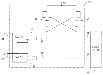
Controls;
U.S. Pat. Apl. Ser. No. not yet assigned, filed on date even herewith,
entitled Nanotube-Based Transfer Devices and Related Circuits,-
U.S. Pat. Apl. Ser. No. not yet assigned, filed on date even herewith,
entitled Integrated Nanotube and Field Effect Switching Device;
U.S. Pat. Apl. Ser. No. not yet assigned, filed on date even herewith,
entitled Receiver Circuit Using Nanotube-Based Switches and
Transistors;
U.S. Pat. Apl. Ser. No. not yet assigned, filed on date even herewith,
entitled Nanotube-based Logic Driver Circuits;
U.S. Pat. Api. Ser. No. not yet assigned, filed on date even herewith,
entitled Storage Elements Using Nanotube Switching Elements; and
1
CA 02570416 2006-12-14
WO 2006/033681 PCT/US2005/018536
U.S. Pat. Apl. Ser. No. not yet assigned, filed on date even herewith,
entitled Tri-State Circuit Using Nanotube Switching Elements.
Background
1. Technical Field
[0003] The present application generally relates to nanotube switching
circuits
and in particular to nanotube switching circuits used in receiver circuits.
2. Discussion of Related Art
[0004] Digital logic circuits are used in personal computers, portable
electronic
devices such as personal organizers and calculators, electronic entertainment
devices, and in control circuits for appliances, telephone switching systems,
automobiles, aircraft and other items of manufacture. Early digital logic was
constructed out of discrete switching elements composed of individual bipolar
transistors. With the invention of the bipolar integrated circuit, large
numbers of
individual switching elements could be combined on a single silicon substrate
to
create complete digital logic circuits such as inverters, NAND gates, NOR
gates,
flip-flops, adders, etc. However, the density of bipolar digital integrated
circuits is
limited by their high power consumption and the ability of packaging
technology to
dissipate the heat produced while the circuits are operating. The availability
of
metal oxide semiconductor ("MOS") integrated circuits using field effect
transistor
("FET") switching elements significantly reduces the power consumption of
digital
logic and enables the construction of the high density, complex digital
circuits used
in current technology. The density and operating speed of MOS digital circuits
are
still limited by the need to dissipate the heat produced when the device is
operating.
[0005] Digital logic integrated circuits constructed from bipolar or MOS
devices do not function correctly under conditions of high heat or heavy
radiation.
Current digital integrated circuits are normally designed to operate at
temperatures
less than 100 degrees centigrade and few operate at temperatures over 200
degrees
centigrade. In conventional integrated circuits, the leakage current of the
individual
switching elements in the "off' state increases rapidly with temperature. As
leakage current increases, the operating temperature of the device rises, the
power
2
CA 02570416 2006-12-14
WO 2006/033681 PCT/US2005/018536
consumed by the circuit increases, and the difficulty of discriminating the
off state
from the on state reduces circuit reliability. Conventional digital logic
circuits also
short internally when subjected to heavy radiation because the radiation
generates
electrical currents inside the semiconductor material. It is possible to
manufacture
integrated circuits with special devices and isolation techniques so that they
remain
operational when exposed to heavy radiation, but the high cost of these
devices
limits their availability and practicality. In addition, radiation hardened
digital
circuits exhibit timing differences from their normal counterparts, requiring
additional design verification to add radiation protection to an existing
design.
[0006] Integrated circuits constructed from either bipolar or FET switching
elements are volatile. They only maintain their internal logical state while
power is
applied to the device. When power is removed, the internal state is lost
unless some
type of non-volatile memory circuit, such as EEPROM (electrically erasable
programmable read-only memory), is added internal or external to the device to
maintain the logical state. Even if non-volatile memory is utilized to
maintain the
logical state, additional circuitry is necessary to transfer the digital logic
state to the
memory before power is lost, and to restore the state of the individual logic
circuits
when power is restored to the device. Alternative solutions to avoid losing
information in volatile digital circuits, such as battery backup, also add
cost and
complexity to digital designs.
[0007] Important characteristics for logic circuits in an electronic device
are
low cost, high density, low power, and high speed. Resistance to radiation and
the
ability to function correctly at elevated temperatures also expand the
applicability
of digital logic. Conventional logic solutions are limited to silicon
substrates, but
logic circuits built on other substrates would allow logic devices to be
integrated
directly into many manufactured products in a single step, further reducing
cost.
[0008] Devices have been proposed which use nanoscopic wires, such as
single-walled carbon nanotubes, to form crossbar junctions to serve as memory
cells. See WO 01/03208, Nanoscopic Wire-Based Devices, Arrays, and Methods
of Their Manufacture; and Thomas Rueckes et al., "Carbon Nanotube-Based
Nonvolatile Random Access Memory for Molecular Computing," Science, vol.
289, pp. 94-97, 7 July, 2000.) Hereinafter these devices are called nanotube
wire
3
CA 02570416 2006-12-14
WO 2006/033681 PCT/US2005/018536
crossbar memories (NTWCMs). Under these proposals, individual single-walled
nanotube wires suspended over other wires define memory cells. Electrical
signals
are written to one or both wires to cause them to physically attract or repel
relative
to one another. Each physical state (i.e., attracted or repelled wires)
corresponds to
an electrical state. Repelled wires are an open circuit junction. Attracted
wires are
a closed state forming a rectified junction. When electrical power is removed
from
the junction, the wires retain their physical (and thus electrical) state
thereby
forming a non-volatile memory cell.
[0009] U.S. Patent Publication No. 2003-0021966 discloses, among other
things, electromechanical circuits, such as memory cells, in which circuits
include a
structure having electrically conductive traces and supports extending from a
surface of a substrate. Nanotube ribbons that can electromechanically deform,
or
switch are suspended by the supports that cross the electrically conductive
traces.
Each ribbon comprises one or more nanotubes. The ribbons are typically formed
from selectively removing material from a layer or matted fabric of nanotubes.
[0010] For example, as disclosed in U.S. Patent Publication No. 2003-0021966,
a nanofabric may be patterned into ribbons, and the ribbons can be used as a
component to create non-volatile electromechanical memory cells. The ribbon is
electromechanically-deflectable in response to electrical stimulus of control
traces
and/or the ribbon. The deflected, physical state of the ribbon may be made to
represent a corresponding information state. The deflected, physical state has
non-
volatile properties, meaning the ribbon retains its physical (and therefore
informational) state even if power to the memory cell is removed. As explained
in
U.S. Patent Publication No. 2003-0124325, three-trace architectures may be
used
for electromechanical memory cells, in which the two of the traces are
electrodes to
control the deflection of the ribbon.
[0011] The use of an electromechanical bi-stable device for digital
information
storage has also been suggested (c.f. US4979149: Non-volatile memory device
including a micro-mechanical storage element).
[0012] The creation and operation of bi-stable, nano-electro-mechanical
switches based on carbon nanotubes (including mono-layers constructed thereof)
4
CA 02570416 2010-08-05
69675-800
and metal electrodes has been detailed in a previous patent application of
Nantero,
Inc. (U.S. Patent Nos. 6574130, 6643165, 6706402; U.S. Patent Apl. Ser. Nos.
09/915093, 10/033323, 10/033032, 10/128117, 10/341005, 10/341055, 10/341054,
10/341130, 10/776059, and 10/776572.
Summary
[0013] The invention provides receiver circuits using nanotube based switches
and logic.
[0014] Under one aspect of the invention, a receiver circuit includes a
differential input having a first and second input link, and a differential
output
having a first and second output link. First, second, third and fourth
switching
elements each have an input node, an output node, a nanotube channel element,
and
a control structure disposed in relation to the nanotube channel element to
controllably form and unform an electrically conductive channel between said
input
node and said output node. The control structure of the first switching
element is in
electrical communication with the first input link, and the input node is in
electrical
communication with a low reference voltage. The output node is in electrical
communication with the first output link. The control structure of the second
switching element in electrical communication with the second input link, and
the
input node is in electrical communication with a low reference voltage, and
the
output node is in electrical communication with the second output link. The
output
node of the third switching element is in electrical communication with the
first
output link, and the control structure is in electrical communication with the
second
output link and the input node is in electrical communication a high reference
voltage. The output node of the fourth switching element is in electrical
communication with the second output link, and the control structure is in
electrical
communication with the first output link and the input node is in electrical
communication a high reference voltage.
[0015] Under another aspect of the invention, the control structure of the
first
and second switching elements includes a control (set) electrode and a release
CA 02570416 2006-12-14
WO 2006/033681 PCT/US2005/018536
electrode, and the first input link is coupled to the control (set) electrode
of the first
switching element and the release electrode of the second switching element.
The
second input link is coupled to the control (set) electrode of the second
switching
element and the release electrode of the first switching element.
[0016] Under another aspect of the invention, the control structure of the
third
and fourth switching elements includes a control (set) electrode and a release
electrode, and the first output link is coupled to the control (set) electrode
of the
fourth switching element. The second output link is coupled to the control
(set)
electrode of the third switching element, and the release electrodes of the
third and
fourth switching elements are coupled to the high reference voltage.
6
CA 02570416 2006-12-14
WO 2006/033681 PCT/US2005/018536
Brief Description of the Drawings
[0017] Figure 1 depicts a receiver circuit according to certain embodiments of
the invention;
[0018] Figures 2A-D illustrate nanotube switches as used in certain
embodiments of the invention;
[0019] Figures 3A-C depict the notation used to describe the nanotube switch
and its states; and
[0020] Figures 4A-B depict the operation of the receiver circuit shown in
Figure 1.
Detailed Description
[0021] Preferred embodiments of the invention provide a receiver circuit that
uses nanotube-based switches. Preferably, the circuits are dual-rail
(differential).
The receiver circuit can sense small voltage inputs and convert them to larger
voltage swings.
[0022] Figure 1 depicts a preferred receiver circuit 10. As illustrated the
receiver circuit 10 receives differential input signal AT and Ac on links 25
and 25'
and provides a differential signal to other logic 45 via links 32 and 32'.
[0023] Receiver 10 includes non-volatile nanotube switches 15 and 20, and
non-volatile nanotube switch pull-up devices 35 and 40. The outputs 30 and 30'
of
nanotube switches 15 and 20 are connected to the outputs of pull-up switches
35
and 40. AT is coupled to the control electrode (more below) of nanotube switch
15
and Ac is coupled to the release electrode (more below). Ac is coupled to the
control electrode of nanotube switch 20 and AT is coupled to the release
electrode.
Each nanotube switch 15 and 20 has its signal electrode (more below) coupled
to
ground. The outputs 30 and 30' are cross-coupled to the control electrodes of
the
pull-up switches 35 and 40 as depicted. The release electrodes of each pull-up
switch are tied to the nanotube channel element and signal electrode of the
switch,
7
CA 02570416 2010-08-05
69675-800
as depicted. The signal electrode is tied to Vdd in this embodiment. The pull-
up
switches 35 and 40 are sized to be volatile devices.
[0024] Figures 2A-D depict a preferred nanotube switching element 100 in
cross-section and layout views and in two informational states. These switches
may
be used for switches 15 and 20 of Figure 1. A more detailed description of
these
switches may be found in the related cases identified above. A
brief description follows here for convenience.
[0025] Figure 2A is a cross sectional view of a preferred nanotube switching
element 100. Nanotube switching element includes a lower portion having an
insulating layer 117, control electrode 111, output electrodes 113c,d.
Nanotube
switching element further includes an upper portion having release electrode
112,
output electrodes 113a,b, and signal electrodes 114a,b. A nanotube channel
element 115 is positioned between and held by the upper and lower portions.
[0026] Release electrode 112 is made of conductive material and is separated
from nanotube channel element 115 by an insulating material 119. The channel
element 115 is separated from the facing surface of insulator 119 by a gap
height
G102.
[0027] Output electrodes 113a,b are made of conductive material and are
separated from nanotube channel element 115 by insulating material 119.
[0028] Output electrodes 113c,d are likewise made of conductive material and
are separated from nanotube channel element 115 by a gap height G103. Notice
that the output electrodes 113c,d are not covered by insulator.
[0029] Control electrode 111 is made of conductive material and is separated
from nanotube channel element 11-5 by an insulating layer (or film) 118. The
channel element 115 is separated from the facing surface of insulator 118 by a
gap
height G 104.
[0030] Signal electrodes 114a,b each contact the nanotube channel element 115
and can therefore supply whatever signal is on the signal electrode to the
channel
element 115. This signal may be a fixed reference signal (e.g., Vdd or Ground)
or
8
CA 02570416 2006-12-14
WO 2006/033681 PCT/US2005/018536
varying (e.g., a Boolean discrete value signal that can change). Only one of
the
electrodes 1 14a,b need be connected, but both may be used to reduce effective
resistance.
[0031] Nanotube channel element 115 is a lithographically-defined article made
from a porous fabric of nanotubes (more below). It is electrically connected
to
signal electrodes 1 14a,b. The electrodes 1 14a,b and support 116 pinch or
hold the
channel element 115 at either end, and it is suspended in the middle in spaced
relation to the output electrodes 113a-d and the control electrode 111 and
release
electrode 112. The spaced relationship is defined by the gap heights G102-G104
identified above. For certain embodiments, the length of the suspended portion
of
channel element 115 is about 300 to 350 nm.
[0032] Under certain embodiments the gaps G103, G104, G102 are in the range
of 5 - 30 nm. The dielectric on terminals 112, 111, and 113a and 113b are in
the
range of 5 - 30 nm, for example. The carbon nanotube fabric density is
approximately 10 nanotubes per 0.2 x 0.2 um area, for example. The suspended
length of the nanotube channel element is in the range of 300 to 350 nm, for
example. The suspended length to gap ratio is about 5 to 15 to 1 for non-
volatile
devices, and less than 5 for volatile operation, for example.
[0033] Figure 2B is a plan view or layout of nanotube switching element 100.
As shown in this figure, electrodes 113b,d are electrically connected as
depicted by
the notation `X' and item 102. Likewise electrodes 113a,c are connected as
depicted by the 'X'. In preferred embodiments the electrodes are further
connected
by connection 120. All of the output electrodes collectively form an output
node
113 of the switching element 100.
[0034] Under preferred embodiments, the nanotube switching element 100 of
Figures 2A and 2B operates as shown in Figures 2C and D. Specifically,
nanotube
switching element 100 is in an OPEN (OFF) state when nanotube channel element
is in position 122 of Figure 1C. In such state, the channel element 115 is
drawn
into mechanical contact with dielectric layer 119 via electrostatic forces
created by
the potential difference between electrode 112 and channel element 115. Output
electrodes 113a,b are in mechanical contact (but not electrical contact) with
channel
9
CA 02570416 2010-08-05
69675-800
element 115. Nanotube switching element 100 is in a CLOSED (ON) state when
channel element 115 is elongated to position 124 as illustrated in Figure 1D.
In
such state, the channel element 115 is drawn into mechanical contact with
dielectric
layer 118 via electrostatic forces created by the potential difference between
electrode 111 and channel element 115. Output electrodes 113c,d are in
mechanical
contact and electrical contact with channel element 115 at regions 126.
Consequently, when channel element 115 is in position 124, signal electrodes
114a
and 114b are electrically connected with output terminals 113c,d via channel
element 115, and the signal on electrodes 114 a,b may be transferred via the
channel (including channel element 115) to the output electrodes 113c,d.
[0035] By properly tailoring the geometry of nanotube switching element 100,
the nanotube switching element 100 may be made to behave as a non-volatile or
a
volatile switching element. By way of example, the device state of Figure 2D
may
be made to be non-volatile by proper selection of the length of the channel
element
relative to the gap G104. (The length and gap are two parameters in the
restoring
force of the elongated, deflected channel -element 115.) Length to gap ratios
of
greater than 5 and less than 15 are preferred for non-volatile device; length
to gap
ratios of less than 5 are preferred for volatile devices.
[0036] The nanotube switching element 100 operates in the following way. If
signal electrode 114 and control electrode 111 (or 112) have a potential
difference
that is sufficiently large (via respective signals on the electrodes), the
relationship
of signals will create an electrostatic force that is sufficiently large to
cause the
suspended, nanotube channel element 115 to deflect into mechanical contact
with
electrode 111 (or 112). (This aspect of operation is described in the
patent references.) This deflection is depicted in Figure 2D (and 2C). The
attractive force streches and deflects the nanotube fabric of channel element
115
until it contacts the insulated region 118 of the electrode 111. The nanotube
channel element is thereby strained, and there is a restoring tensil force,
dependent
on the geometrical relationship of the circuit, among other things.
[0037] By using appropriate geometries of components, the switching element
100 then attains the closed, conductive state of Figure 1D in which the
nanotube
channel 115 mechanically contacts the control electrode 111 and also output
CA 02570416 2006-12-14
WO 2006/033681 PCT/US2005/018536
electrode 11 3c,d. Since the control electrode 111 is covered with insulator
118 any
signal on electrode 114 is transferred from the electrode 114 to the output
electrode
113 via the nanotube channel element 115. The signal on electrode 114 may be a
varying signal, a fixed signal, a reference signal, a power supply line, or
ground
line. The channel formation is controlled via the signal applied to the
electrode 111
(or 112). Specifically the signal applied to control electrode 111 needs to be
sufficiently different in relation to the signal on electrode 114 to create
the
electrostatic force to deflect the nanotube channel element to cause the
channel
element 115 to deflect and to form the channel between electrode 114 and
output
electrode 113, such that switching element 100 is in the CLOSED (ON) state.
[0038] In contrast, if the relationship of signals on the electrode 114 and
control
electrode 111 is insufficiently different, then the nanotube channel element
115 is
not deflected and no conductive channel is formed to the output electrode 113.
Instead, the channel element 115 is attracted to and physically contacts the
insulation layer on release electrode 112. This OPEN (OFF) state is shown in
Figure 2C. The nanotube channel element 115 has the signal from electrode 114
but this signal is not transferred to the output node 113. Instead, the state
of the
output node 113 depends on whatever circuitry it is connected to and the state
of
such circuitry. The state of output node 113 in this regard is independent of
channel
element voltage from signal electrode 114 and nanotube channel element 115
when
the switching element 100 is in the OPEN (OFF) state.
[0039] If the voltage difference between the control electrode 111 (or 112)
and
the channel element 115 is removed, the channel element 115 returns to the non-
elongated state (see Figure 2A) if the switching element 100 is designed to
operate
in the volatile mode, and the electrical connection or path between the
electrode 115
to the output node 113 is opened.
[0040] Preferably, if the switching element 100 is designed to operate in the
non-volatile mode, the channel element is not operated in a manner to attain
the
state of Figure 1A. Instead, the electrodes 111 and 112 are expected to be
operated
so that the channel element 115 will either be in the state of Figure 2C or
2D.
11
CA 02570416 2006-12-14
WO 2006/033681 PCT/US2005/018536
[0041] The output node 113 is constructed to include an isolation structure in
which the operation of the channel element 115 and thereby the formation of
the
channel is invariant to the state of the output node 113. Since in the
preferred
embodiment the channel element is electromechanically deflectable in response
to
electrostatically attractive forces, an output node 113 in principle could
have any
potential. Consequently, the potential on an output node may be sufficiently
different in relation to the state of the channel element 115 that it would
cause
deflection of the channel element 115 and disturb the operation of the
switching
element 100 and its channel formation; that is, the channel formation would
depend
on the state of the output node. In the preferred embodiment this problem is
addressed with an output node that includes an isolation structure to prevent
such
disturbances from being caused.
[0042] Specifically, the nanotube channel element 115 is disposed between two
oppositely disposed electrodes 113b,d (and also 113 a,c) of equal potential.
Consequently, there are equal but opposing electrostatic forces that result
from the
voltage on the output node. Because of the equal and opposing electrostatic
forces,
the state of output node 113 cannot cause the nanotube channel element 115 to
deflect regardless of the voltages on output node 113 and nanotube channel
element
115. Thus, the operation and formation of the channel is made invariant to the
state
of the output node.
[0043] Under certain embodiments of the invention, the nanotube switching
element 100 of Figure 2A may be used as pull-up and pull-down devices to form
power-efficient circuits. Unlike MOS and other forms of circuits, the pull-up
and
pull down devices may be identical devices and need not have different sizes
or
materials. To facilitate the description of such circuits and to avoid the
complexity
of the layout and physical diagrams of Figures IA-D, a schematic
representation
has been developed to depict the switching elements.
[0044] Figure 3A is a schematic representation of a nanotube switching element
100 of Figure 2A. The nodes use the same reference numerals. The nanotube
switching element 100 may be designed to operate in the volatile or non-
volatile
switching mode. In this example, a non-volatile switching mode is used as
illustrated by switches 15 and 20 in Figure 1.
12
CA 02570416 2006-12-14
WO 2006/033681 PCT/US2005/018536
[0045] Figures 3B-C depict a nanotube channel element 100 when its signal
electrodes is tied to ground, and its states of operation. For example, Figure
3B is a
schematic representation of the nanotube switching element in the OPEN (OFF)
state illustrated in Figure 2C, in which node 114 and the nanotube channel
element
115 are at ground, the control electrode 111 is at ground, and the release
electrode
112 is at Vdd. The nanotube channel element is not in electrical contact with
output
node 113, but instead is depicted by the short black line 203 representing the
nanotube element contacting insulator 119. Figure 3C is a schematic
representation
of the switching element in the CLOSED (ON) state illustrated in Figure 2D. In
this case, signal node 114 and the nanotube channel element 115 are at ground,
the
control electrode 111 is at Vdd, and the release electrode 112 is at ground.
The
nanotube channel element is deflected into mechanical and electrical contact
with
the output node 113. Moreover, if as described above, geometries are selected
appropriately, the contact will be non-volatile as a result of the Van der
Waals
forces between the channel element and the uninsulated, output electrode.) The
state of electrical contact is depicted by the short black line 204
representing the
nanotube channel element contacting the output terminal 113. This results in
the
output node 113 assuming the same signal (i.e., Vdd) as the nanotube channel
element 115 and signal node 114. The switches 15 and 20 operate analogously
but
opposite when the signal electrode is tied to Vdd.
[0046] Figure 3A' is a schematic representation of a nanotube switching
element 100 of Figure 2A designed to be used in a volatile operating mode with
release electrode connected to the nanotube switching element through the
switching node contacting the nanotube element as illustrated by switches 35
and
40 in Figure 1. The nodes use the same reference numerals plus a prime (').
Also,
the release electrode is electrically connected to the nanotube contact such
that there
is no voltage difference between release electrode and the nanotube channel
element. The arrow is used to show the mechanical force and direction on the
nanotube channel element 115. For example, as depicted, the channel element
has a
bias away from electrode 111, i.e., if the channel element 115 were deflected
into
contact with electrode 111 a mechanical restoring force would be in the
direction of
the arrow.
13
CA 02570416 2006-12-14
WO 2006/033681 PCT/US2005/018536
[0047] Figures 3B'-C' depict a nanotube channel element 100 when its signal
electrodes are tied to VDD, and its states of operation. For example, Figure
3B' is a
schematic representation of the nanotube switching element in the OPEN (OFF)
state illustrated in Figure 2C, in which node 114' and the nanotube channel
element
115' are at VDD, the release electrode 112' is electrically connected to node
114'
and is therefore also at VDD, and the control electrode 111' is also at VDD.
The
nanotube channel element is not in electrical contact with output node 113,
but
instead is in a non-extended position, restored by the mechanical restoring
force
indicated by the arrow in Figure 2B'. Figure 3C' is a schematic representation
of
the switching element in the CLOSED (ON) state illustrated in Figure 2D. In
this
case, signal node 114' and the nanotube channel element 115' are at VDD, the
release electrode 112' is electrically connected to signal node 114' and is
therefore
also at VDD, and the control electrode 111' is at ground. The nanotube channel
element is deflected into mechanical and electrical contact with the output
node
113. Moreover, if as described above, geometries are selected appropriately,
the
contact will be volatile and the channel element will remain in contact with
the
uninsulated output electrode until the electrostatic force is removed, and
then the
mechanical restoring force in the direction of the arrow will overcome the van
der
Waals forces and release nanotube channel element from contact with the output
electrode. The state of the volatile electrical contact is depicted by the
short black
line 204' representing the nanotube channel element contacting the output
terminal
113'. This results in the output node 113' assuming the same signal (i.e.,
Vdd) as
the nanotube channel element 115' and signal node 114'. The switches 35 and 40
operate analogously but opposite when the signal electrode is tied to ground.
[0048] Receiver 10 is designed with non-volatile nanotube switches 15 and 20,
and volatile nanotube switches 35 and 40. Non-volatile switches 15 and 20 are
designed such that the mechanical restoring forces that result from the
nanotube
elongation after switching are weaker than the van der Waals restraining
forces. An
electrostatic voltage is used (required) to change the state of the nanotube
from
"ON" (CLOSED) to "OFF" (OPEN), and "OFF" to "ON." Volatile switches 35
and 40 have the release plate electrically connected to the nanotube contact
so that
there is no electrostatic restoring force. Volatile devices 35 and 40 are
designed
such that the mechanical restoring forces that result from the nanotube
elongation
14
CA 02570416 2006-12-14
WO 2006/033681 PCT/US2005/018536
after switching are stronger than the van der Waals restraining forces, and
the
volatile nanotube will return to from the "ON" state to the "OFF" state once
the
electrostatic field is removed (the difference voltage between the input
electrode
and the nanotube fabric goes to zero). The direction of the mechanical
restoring
force is indicated by an arrow in the symbol for volatile nanotube switches 35
and
40. The nanotube contact of each of the non-volatile switches 15 and 20 is
connected to ground (reference voltage VREF = 0).
[0049] Figure 4A illustrates the operation of receiver 10 shown in Figure 1
when input voltage VAt = VRED, a positive voltage, and complementary voltage
VAc = 0. VRED is not necessarily the same as VDD, and may be lower than VDD,
for example. The nanotube threshold voltage of nonvolatile nanotube switches
15
and 20 is set to activate the switches to the "ON" or "OFF" state in response
to
voltage VRED. That is, voltage difference of VRED or higher across the control
node and nanotube channel element is sufficient to make the switch contact the
output node and form a channel between the signal node and the output node.
For
the applied conditions illustrated in Figure 4A, the voltage difference
between the
input gate and the nanotube channel element of nonvolatile nanotube switch 15
forces the nanotube channel element in contact with the output electrode and
output
30 is thus connected to ground (i.e., the voltage on the signal electrode of
switch
15). Also, the voltage difference between release gate and the nanotube
channel
element of nonvolatile nanotube switch 20 forces the nanotube channel element
in
contact with the dielectric layer on the opposing output electrode, and output
30' is
in an open state. If volatile nanotube switch 40 is in the "ON" state at the
time, a
current will flow briefly from power supply VDD to ground through switches 40
and 15. The resistance RNT of the nanotube channel element is chosen such that
the RNT of switch 15 is substantially lower than RNT of switch 40 so that
output
30 is held near ground voltage. RNT for switch 15 is chosen to be 3 to 5 time
smaller than RNT for switch 40. If switch 40 has a width of 10 parallel carbon
nanotubes (NT fibers), then switch 15 is chosen to have a width of 30 to 50
parallel
NT fibers, for example. When output 30 is forced to near zero volts, the input
of
switch 35 is forced to near zero volts and switch 35 turns "ON." The input
voltage
of switch 40 transitions from zero to VDD, reducing the voltage difference
between
switch 40 input electrode and nanotube element to zero. As the electrostatic
force
CA 02570416 2006-12-14
WO 2006/033681 PCT/US2005/018536
between input electrode and nanotube goes to zero, the mechanical restoring
force
turns switch 40 "OFF" and current stops through switches 40 and 15. Receiver
10
is in a state 10' illustrated in Figure 4B. Logic gates 45 input 32 is at zero
volts,
and input 32' is at VDD. Output 30' is at VDD, but no current flows because
switch 20 is in the "OFF" (OPEN) position (state).
[0050] Figure 4B illustrates the operation of receiver 10 shown in Figure 1
when input voltage VAt equals zero, and complementary voltage VAc = VRED, a
positive voltage. VRED is not necessarily the same as VDD, and may be lower
than
VDD, for example. The nanotube threshold voltage of nonvolatile nanotube
switches 15 and 20 is set to activate the switches to the "ON" or "OFF" state
in
response to voltage VRED. For the applied conditions illustrated in Figure 4B,
the
voltage difference between the input gate and the nanotube fabric of
nonvolatile
nanotube switch 20 forces the nanotube channel element in contact with the
output
electrode, and output 30' is connected to ground. Also, the voltage difference
between release gate and the nanotube channel element of nonvolatile nanotube
switch 15 forces the nanotube channel element in contact with the dielectric
layer
on the opposing electrode, and output 30 is in an open state. If volatile
nanotube
switch 35 is in the "ON" state at the time, a current will flow briefly from
power
supply VDD to ground through switches 35 and 20. Nanotube resistance RNT is
chosen such that the RNT of switch 20 is substantially lower than RNT of
switch 35
so that output 30' is held near ground voltage. RNT for switch 20 is chosen to
be 3
to 5 time smaller than RNT for switch 35. If switch 35 has a width of 10
parallel
NT fibers, then switch 20 is chosen to have a width of 30 to 50 parallel NT
fibers,
for example. When output 30' is forced to near zero volts, the input of switch
40 is
forced to near zero volts and switch 40 turns "ON." The input voltage of
switch 35
transitions from zero to VDD, reducing the voltage difference between switch
35
input electrode and nanotube element to zero. As the electrostatic force
between
input electrode and nanotube goes to zero, the mechanical restoring force
turns
switch 35 "OFF" and current stops through switches 40 and 15. Receiver 10 is
in a
state 10" illustrated in Figure 4B. Logic gates 45 input 32 is at VDD volts,
and
input 32' is at zero. Output 30 is at VDD, but no current flows because switch
15 is
in the "OFF" (OPEN) position (state).
16
CA 02570416 2010-08-05
69675-800
[0051] Several of the related patent references describe alternative
variations of nanotube-based switches. Many of these may be incorporated into
the
embodiments described above, providing volatile or non-volatile behavior,
among
other things. Likewise the fabrication techniques taught in such cases may be
utilized here as well.
[0052] Nanotube-based logic may be used in conjunction with and in the
absence of diodes, resistors and transistors or as part of or a replacement to
CMOS,
biCMOS, bipolar and other transistor level technologies. Also, the non-
volatile flip
flop may be substitued for an SRAM flip flop to create a NRAM cell. The
interconnect wiring used to interconnect the nanotube device terminals may be
conventional wiring such as AlCu, W, or Cu wiring with appropriate insulating
layers such as Si02, polyimide, etc, or may be single or multi-wall nanotubes
used
for wiring.
[0053] There is no significant leakage current between input and output
terminals in the "OFF' state of the nanotube-based switch, and there is no
junction
leakage. Therefore the nanotube-based switch may operate in harsh environments
such as elevated temperatures, e.g., 150 to 200 deg-C or higher. There is no
alpha
particle sensitivity.
[0054] While single walled carbon nanotubes are preferred, multi-walled
carbon nanotubes may be used. Also nanotubes may be used in conjunction with
nanowires. Nanowires as mentioned herein is meant to mean single nanowires,
aggregates of non-woven nanowires, nanoclusters, nanowires entangled with
nanotubes comprising a nanofabric, mattes of nanowires, etc. The invention
relates
to the generation of nanoscopic conductive elements used for any electronic
application.
[0055] The following patent references refer to various techniques for
creating
nanotube fabric articles and switches and are assigned to the assignee of this
application:
U.S. Pat. Apl. Ser. No. 10/341,005, filed on January 13, 2003, entitled
Methods of Making Carbon Nanotube Films, Layers, Fabrics, Ribbons,
Elements and Articles;
17
CA 02570416 2006-12-14
WO 2006/033681 PCT/US2005/018536
U.S. Pat. Apl. Ser. No. 09/915,093, filed on July 25, 2001, entitled
Electromechanical Memory Array Using Nanotube Ribbons and Method
for Making Same;
U.S. Pat. Apl. Ser. No. 10/033,032, filed on December 28, 2001, entitled
Methods of Making Electromechanical Three-Trace Junction Devices;
U.S. Pat. Apl. Ser. No. 10/033,323, filed on December 28, 2001, entitled
Electromechanical Three-Trace Junction Devices;
U.S. Pat. Apl. Ser. No. 10/128,117, filed on April 23, 2002, entitled
Methods of NT Films and Articles;
U.S. Pat. Apl. Ser. No. 10/341,055, filed January 13, 2003, entitled
Methods of Using Thin Metal Layers to Make Carbon Nanotube Films,
Layers, Fabrics, Ribbons, Elements and Articles;
U.S. Pat. Apl. Ser. No. 10/341,054, filed January 13, 2003, entitled
Methods of Using Pre formed Nanotubes to Make Carbon Nanotube
Films, Layers, Fabrics, Ribbons, Elements and Articles;
U.S. Pat. Apl. Ser. No. 10/341,130, filed January 13, 2003, entitled
Carbon Nanotube Films, Layers, Fabrics, Ribbons, Elements and
Articles;
U.S. Pat. Apl., Ser. No. 10/776,059, filed February 11, 2004, entitled
Devices Having Horizontally-Disposed Nanofabric Articles and
Methods of Making The Same; and
U.S. Pat. Apl., Ser. No. 10/776,572, filed February 11, 2004, entitled
Devices Having Vertically-Disposed Nanofabric Articles and Methods
of Making the Same.
18
CA 02570416 2006-12-14
WO 2006/033681 PCT/US2005/018536
[0056] Volatile and non-volatile switches, and switching elements of numerous
types of devices, can be thus created. In certain preferred embodiments, the
articles
include substantially a monolayer of carbon nanotubes. In certain embodiments
the
nanotubes are preferred to be single-walled carbon nanotubes. Such nanotubes
can
be tuned to have a resistance between 0.2- 100 kOhm/^ or in some cases from
100
kOhm/^ to 1GOhm/^.
[0057] The receiver circuit facilitates compatibility between carbon nanotube
logic circuits and CMOS logic. For example, the output of conventional CMOS
circuits may drive nanotube-based switches. Dual-rail (differential) logic
inputs are
used and the receiver circuit may operate in a differential sensing mode, at
smaller
voltage swings for high speed and lower power dissipation, with no internal
logic
reference level needed at the receiving end. The output of the receiver
circuit is a
voltage selected for desired (e.g., optimum) on chip circuit operation.
Consequently, the receiver circuit may operate at a different voltage than
CMOS
logic circuits. Preferred receiver circuits enable a nanotube logic chip or an
embedded nanotube logic function using only nanotube logic to interface
directly
with CMOS circuits driving the receiver inputs, with input voltage signals
that may
be different from on chip voltage signals. Also, preferred receiver circuits
enables
integrated logic blocks using CMOS and combined nanotube-based logic and
CMOS technologies to operate at different power supply voltages in the same
system on separate chips, or integrated on the same chip. Such a receiver, and
other
combined circuits, may be used to facilitate the introduction of nanotube-
based
logic in a CMOS environment.
[0058] The nanotube switching element of preferred embodiments utilizes
multiple controls for the formation and unformation of the channel. In some
embodiments, the device is sized to create a non-volatile device and one of
the
electrodes may be used to form a channel and the other may be used to unform a
channel. The electrodes may be used as differential dual-rail inputs.
Alternatively
they may be set and used at different times. For example, the control
electrode may
be used in the form of a clock signal, or the release electrode may be used as
a form
of clocking signal. Also, the control electrode and release electrode may be
placed
19
CA 02570416 2006-12-14
WO 2006/033681 PCT/US2005/018536
at the same voltage, for example, such that the state of the nanotube cannot
be
disturbed by noise sources such as voltage spikes on adjacent wiring nodes.
[0059] A Figure 2 device may be designed to operate as a volatile or non-
volatile device. In the case of a volatile device, the mechanical restoring
force due
to nanotube elongation is stronger than the van der Waals retaining force, and
the
nanotube mechanical contact with a control or release electrode insulator is
broken
when the electrical field is removed. Typically, nanotube geometrical factors
such
as suspended length to gap ratios of less than 5 to 1 are used for volatile
devices. In
the case of a non-volatile device, the mechanical restoring force due to
nanotube
elongation is weaker than the van der Waals retaining force, and the nanotube
mechanical contact with a control or release electrode insulator remains un-
broken
when the electric field is removed. Typically, nanotube geometrical factors
such as
suspended length to gap ratios of greater than 5 to 1 and less than 15 to 1
are used
for non-volatile devices. An applied electrical field generating an
electromechanical
force is required to change the state of the nanotube device. Van der Waals
forces
between nanotubes and metals and insulators are a function of the material
used in
the fabrication nanotube switches. By way of example, these include insulators
such
as silicon dioxide and silicon nitride, metals such as tungsten, aluminum,
copper,
nickel, palladium, and semiconductors such as silicon. For the same surface
area,
forces will vary by less than 5% for some combinations of materials, or may
exceed
2X for other combinations of materials, so that the volatile and non-volatile
operation is determined by geometrical factors such as suspended length and
gap
dimensions and materials selected. It is, however, possible to design devices
by
choosing both geometrical size and materials that exhibit stronger or weaker
van
der Waals forces. By way of example, nanotube suspended length and gap height
and fabric layer density, control electrode length, width, and dielectric
layer
thickness may be varied. Output electrode size and spacing to nanotube may be
varied as well. Also, a layer specifically designed to increase van der Waals
forces
(not shown) may be added during the fabrication nanotube switching element 100
illustrated in Figure 1. For example, a thin (5 to 10 nm, for example) layer
of metal
(not electrically connected), semiconductor (not electrically connected), or
insulating material may be added (not shown) on the insulator layer associated
with
control electrode 111 or release electrode 112 that increases the van der
Waals
CA 02570416 2006-12-14
WO 2006/033681 PCT/US2005/018536
retaining force without substantial changes to device structure for better non-
volatile operation. In this way, both geometrical sizing and material
selection are
used to optimize device operation, in this example to optimize non-volatile
operation.
[0060] In a complementary circuit such as an inverter using two nanotube
switching elements 100 with connected output terminals, there can be momentary
current flow between power supply and ground in the inverter circuit as the
inverter
changes from one logic state to another logic state. In CMOS, this occurs when
both PFET and NFET are momentarily ON, both conducting during logic state
transition and is sometimes referred to as "shoot-through" current. In the
case of
electromechanical inverters, a momentary current may occur during change of
logic
state if the nanotube fabric of a first nanotube switch makes conductive
contact with
the first output structure before the nanotube fabric of a second nanotube
switch
releases conductive contact with the second output structure. If, however, the
first
nanotube switch breaks contact between the first nanotube fabric and the first
output electrode before the second nanotube switch makes contact between the
second nanotube fabric and the second output electrode, then a break-before-
make
inverter operation occurs and "shoot-through" current is minimized or
eliminated.
Electromechanical devices that favor break-before-make operation may be
designed
with different gap heights above and below the nanotube switching element, for
example, such that forces exerted on the nanotube switching element by control
and
release electrodes are different; and/or travel distance for the nanotube
switching
element are different in one direction than another; and/or materials are
selected
(and/or added) to increase the van der Waals forces in one switching direction
and
weakening van der Waals forces in the opposite direction.
[0061] By way of example, nanotube switching element 100 illustrated in
Figure 1 may be designed such that gap G102 is substantially smaller (50%
smaller,
for example) than gap G104. Also, gap G103 is made bigger such that nanotube
element 115 contact is delayed when switching. Also, dielectric thicknesses
and
dielectric constants may be different such that for the same applied voltage
differences, the electric field between release electrode 112 and nanotube
element
115 is stronger than the electric field between control electrode 111 and
nanotube
21
CA 02570416 2006-12-14
WO 2006/033681 PCT/US2005/018536
element 115, for example, to more quickly disconnect nanotube element 115 from
output terminals 11 3c and 11 3d. Output electrodes 11 3c and 11 3d may be
designed
to have a small radius and therefore a smaller contact area in a region of
contact
with nanotube element 115 compared with the size (area) of contact between
nanotube element 115 and the insulator on control terminal 111 to facilitate
release
of contact between nanotube element 115 and output electrodes 113c and 1 13d.
The
material used for electrodes 113c and 113d may be selected to have weaker van
der
Waals forces respect to nanotube element 115 than the van der Waals forces
between nanotube element 115 and the insulator on release electrode 112, for
example. These, and other approaches, may be used to design a nanotube
switching
element that favors make-before-break operation thus minimizing or eliminating
"shoot-through" current as circuits such as inverters switch from one logic
state to
another.
[0062] The material used in the fabrication of the electrodes and contacts
used
in the nanotube switches is dependent upon the specific application, i.e.
there is no
specific metal necessary for the operation of the present invention.
[0063] Nanotubes can be functionalized with planar conjugated hydrocarbons
such as pyrenes which may then aid in enhancing the internal adhesion between
nanotubes within the ribbons. The surface of the nanotubes can be derivatized
to
create a more hydrophobic or hydrophilic environment to promote better
adhesion
of the nanotube fabric to the underlying electrode surface. Specifically,
functionalization of a wafer/substrate surface involves "derivitizing" the
surface of
the substrate. For example, one could chemically convert a hydrophilic to
hydrophobic state or provide functional groups such as amines, carboxylic
acids,
thiols or sulphonates to alter the surface characteristics of the substrate.
Functionalization may include the optional primary step of oxidizing or ashing
the
substrate in oxygen plasma to remove carbon and other impurities from the
substrate surface and to provide a uniformly reactive, oxidized surface which
is
then reacted with a silane. One such polymer that may be used is
3-aminopropyltriethoxysilane (APTS). The substrate surface may be derivitized
prior to application of a nanotube fabric.
22
CA 02570416 2006-12-14
WO 2006/033681 PCT/US2005/018536
[0064] The invention may be embodied in other specific forms without
departing from the spirit or essential characteristics thereof. The present
embodiments are therefore to be considered in respects as illustrative and not
restrictive, the scope of the invention being indicated by the appended claims
rather
than by the foregoing description, and all changes which come within the
meaning
and range of the equivalency of the claims are therefore intended to be
embraced
therein.
23