Note: Descriptions are shown in the official language in which they were submitted.
CA 02570486 2010-02-05
69675-799
INTEGRATED NANOTUBE AND FIELD EFFECT SWITCHING DEVICE
1
CA 02570486 2006-12-14
WO 2006/078299 PCT/US2005/018535
Background
1. Technical Field
[0003] The present invention generally relates to switching elements and logic
circuits, and in particular to switching elements that integrate nanotube
switching
technology, in which nanotubes provide conductive channels in switches, with
field
effect switching technology and logic circuits formed therefrom.
2. Discussion of Related Art
[0004] Digital logic circuits are used in personal computers, portable
electronic
devices such as personal organizers and calculators, electronic entertainment
devices,
and in control circuits for appliances, telephone switching systems,
automobiles,
aircraft and other items of manufacture. Early digital logic was constructed
out of
discrete switching elements composed of individual bipolar transistors. With
the
invention of the bipolar integrated circuit, large numbers of individual
switching
elements could be combined on a single silicon substrate to create complete
digital
logic circuits such as inverters, NAND gates, NOR gates, flip-flops, adders,
etc.
However, the density of bipolar digital integrated circuits is limited by
their high
power consumption and the ability of packaging technology to dissipate the
heat
produced while the circuits are operating. The availability of metal oxide
semiconductor ("MOS") integrated circuits using field effect transistor
("FET")
switching elements significantly reduces the power consumption of digital
logic and
enables the construction of the high density, complex digital circuits used in
current
technology. The density and operating speed of MOS digital circuits are still
limited
by the need to dissipate the heat produced when the device is operating.
[0005] Digital logic integrated circuits constructed from bipolar or MOS
devices
do not function correctly under conditions of high heat or heavy radiation.
Current
digital integrated circuits are normally designed to operate at temperatures
less than
100 degrees centigrade and few operate at temperatures over 200 degrees
centigrade.
In conventional integrated circuits, the leakage current of the individual
switching
elements in the "off' state increases rapidly with temperature. As leakage
current
increases, the operating temperature of the device rises, the power consumed
by the
2
CA 02570486 2006-12-14
WO 2006/078299 - PCT/US2005/018535
circuit increases, and the difficulty of discriminating the off state from the
on state
reduces circuit reliability. Conventional digital logic circuits also short
internally
when subjected to heavy radiation because the radiation generates electrical
currents
inside the semiconductor material. It is possible to manufacture integrated
circuits
with special devices and isolation techniques so that they remain operational
when
exposed to heavy radiation, but the high cost of these devices limits their
availability
and practicality. In addition, radiation hardened digital circuits exhibit
timing
differences from their normal counterparts, requiring additional design
verification to
add radiation protection to an existing design.
[0006] Integrated circuits constructed from either bipolar or FET switching
elements are volatile. They only maintain their internal logical state while
power is
applied to the device. When power is removed, the internal state is lost
unless some
type of non-volatile memory circuit, such as EEPROM (electrically erasable
programmable read-only memory), is added internal or external to the device to
maintain the logical state. Even if non-volatile memory is utilized to
maintain the
logical state, additional circuitry is necessary to transfer the digital logic
state to the
memory before power is lost, and to restore the state of the individual logic
circuits
when power is restored to the device. Alternative solutions to avoid losing
information in volatile digital circuits, such as battery backup, also add
cost and
complexity to digital designs.
[0007] Important characteristics for logic circuits in an electronic device
are low
cost, high density, low power, and high speed. Resistance to radiation and the
ability
to function correctly at elevated temperatures also expand the applicability
of digital
logic. Conventional logic solutions are limited to silicon substrates, but
logic circuits
built on other substrates would allow logic devices to be integrated directly
into many
manufactured products in a single step, further reducing cost.
[0008] Devices have been proposed which use nanoscopic wires, such as single-
walled carbon nanotubes (NT), to form crossbar junctions to serve as memory
cells.
See WO 01/03208, Nanoscopic Wire-Based Devices, Arrays, and Methods of Their
Manufacture; and Thomas Rueckes et al., "Carbon Nanotube-Based Nonvolatile
Random Access Memory for Molecular Computing," Science, vol. 289, pp. 94-97, 7
July, 2000.) Hereinafter these devices are called nanotube wire crossbar
memories
3
CA 02570486 2006-12-14
WO 2006/078299 PCT/US2005/018535
(NTWCMs). Under these proposals, individual single-walled nanotube wires
suspended over other wires define memory cells. Electrical signals are written
to one
or both wires to cause them to physically attract or repel relative to one
another. Each
physical state (i.e., attracted or repelled wires) corresponds to an
electrical state.
Repelled wires are an open circuit junction. Attracted wires are a closed
state forming
a rectified junction. When electrical power is removed from the junction, the
wires
retain their physical (and thus electrical) state thereby forming a non-
volatile memory
cell.
[0009] U.S. Patent Publication No. 2003-0021966 discloses, among other things,
electromechanical circuits, such as memory cells, using nanotube ribbons. Such
circuits include a structure having electrically conductive traces and
supports
extending from a surface of a substrate. Nanotube ribbons that can
electromechanically deform, or switch, are suspended by the supports that
cross the
electrically conductive traces. Each ribbon comprises one or more nanotubes.
The
ribbons are typically formed by selectively removing material from a layer or
matted
fabric of nanotubes.
[0010] For example, as disclosed in U.S. Patent Publication No. 2003-0021966,
a
nanofabric may be patterned into ribbons, and the ribbons can be used as a
component
to create non-volatile electromechanical memory cells. The ribbon is
electromechanically-deflectable in response to electrical stimulus of control
traces
and/or the ribbon., The deflected, physical state of the ribbon may be made to
represent a corresponding information state. The deflected, physical state has
non-
volatile properties, meaning the ribbon retains its physical (and therefore
informational) state even if power to the memory cell is removed. As explained
in
U.S. Patent Publication No. 2003-0124325, three-trace architectures may be
used for
electromechanical memory cells, in which two of the traces are electrodes to
control
the deflection of the ribbon.
[0011] The use of an electromechanical bi-stable device for digital
information
storage has also been suggested (c.f. US4979149: Non-volatile memory device
including a micro-mechanical storage element).
4
CA 02570486 2010-02-05
69675-799
[0012] The creation and operation of bi-stable, nano-electro-mechanical
switches based on carbon nanotubes (including mono-layers constructed thereof)
and metal electrodes has been detailed in previous patent applications of
Nantero,
Inc. (U.S. Patent Nos. 6,574,130, 6,643,165, 6,706,402, 6,919,592, 6,911,682,
6,784,028, 6,835,591, 7,566,478, 7,560,136, 7,335,395, 7,563,711, 7,259,410,
6,924,538, 7,115,960, and 6,990,009.
SUMMARY OF THE INVENTION
In one broad aspect of the present invention, there is provided an
integrated switching device, comprising: a signal input terminal; an output
terminal; and a control structure including at least one control input
terminal,
electrical stimulation of said control structure controlling formation of a
controllably-formable electrically conductive channel between the signal input
terminal and the output terminal, a first portion of the electrically
conductive
channel including a nanotube channel element and a second portion of the
electrically conductive channel including a field modulatable semiconductor
channel element.
In another broad aspect of the present invention, there is provided
an integrated switching device, comprising: a signal input terminal; an output
terminal; a nanotube switching element, including a nanotube channel element
formed of at least one nanotube, and a nanotube input electrode for providing
a
signal to the nanotube channel element, the nanotube input electrode being
electrically connected to said signal input terminal, and a nanotube output
electrobe for receiving a signal from the nanotube channel element when the
nanotube channel element is activated; a field effect device having a source,
a
drain, and a gate, with a field modulatable channel between the source and the
drain, the source being electrically connected to the output electrode of the
nanotube switching element and the drain being electrically connected to said
output terminal; and a control structure comprising at least one control input
terminal to control formation of a controllably-formable conductive channel
between said signal input terminal and said output terminal, a first portion
of the
5
CA 02570486 2010-02-05
69675-799
conductive channel being formed by the nanotube channel element of the
nanotube switching element, and a second portion of the conductive channel
being formed by the field modulatable channel of the field effect device.
In yet another broad aspect of the present invention, there is
provided an integrated switching device, comprising: a signal input terminal;
an
output terminal; a network of at least one nanotube switching element
electrically
disposed between said signal input terminal and said output terminal; a
network of
at least one field effect device electrically disposed between said signal
input
terminal and said output terminal, said network of at least one field effect
device
being electrically in series with said network of at least one nanotube
switching
element; and a control structure to control formation of a controllably-
formable
conductive channel between said signal input terminal and said output
terminal, a
first portion of the conductive channel being provided by a conductive path
formed
by the network of at least one nanotube switching element and a second portion
of
the conductive channel being provided by a conductive path formed by the
network of at least one field effect device.
5a
CA 02570486 2006-12-14
WO 2006/078299 PCT/US2005/018535
Brief Description of the Drawings
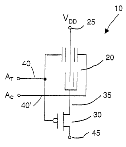
[0013] Figure IA is a schematic representation of an non-volatile integrated
nanotube switching element and PFET device (or NT-PFET device) according to
one
aspect of the invention;
[0014] Figure 1B is a schematic representation of an non-volatile integrated
nanotube switching element and NFET device (or NT-NFET device) according to
one
aspect of the invention;
[0015] Figures 1C and 1D illustrate a cross sectional and plan views of a
nanotube
switching element fabricated according to preferred embodiments of the
invention;
[0016] Figures 1E and IF illustrate cross sectional views of different
positional
and electrical states of a nanotube switching element fabricated according to
preferred
embodiments of the invention;
[0017] Figures 2A-C and 3A-C are schematic representations of nanotube
switching element 100 of Figure 1C in pull-up and pull-down configurations,
respectively;
[0018] Figure 4A is a schematic representation of an inverter constructed
using a
non-volatile integrated NT-PFET device and a non-volatile integrated NT-NFET
device as shown in Figures 1A and 1B, according to one aspect of the
invention;
[0019] Figure 4B is a schematic representation of the inverter of Figure 4A in
one
possible logic state;
[0020] Figure 4C is a schematic representation of the inverter of Figure 4A in
one
possible logic state;
[0021] Figures 4D is a schematic representation of the inverter of Figure 4A
in
one possible logic state;
6
CA 02570486 2006-12-14
WO 2006/078299 PCT/US2005/018535
[0022] Figure 5A is a schematic representation of a dual-rail input and output
non-volatile inverter constructed using non-volatile integrated NT-PFET
devices and
non-volatile integrated NT-NFET devices according to one aspect of the
invention;
[0023] Figure 5B is a schematic representation of the dual-rail inverter of
Figure
5A in one possible logic state; and
[0024] Figure 5C is a schematic representation of the dual-rail inverter of
Figure
5A in one possible logic state.
7
CA 02570486 2006-12-14
WO 2006/078299 PCT/US2005/018535
Summary of the Invention
[0025] Embodiments of the present invention provide integrated switching
devices that combine nanotube (NT) switching elements with field effect
semiconductor elements, including but not limited to MOS NFETs and PFETs
(FETs).
[0026] According to one aspect of the invention, nanotube switching elements
are
integrated with field effect devices to form hybrid switching devices that are
non-
volatile.
[0027] According to one aspect of the invention, an integrated switching
device is
a multi-terminal device, with a signal input terminal, at least one control
input
terminal and an output terminal. An integrated switching device forms and
unforms a
conductive channel from the signal. input to the output subject to the
relative state of
the control input. The conductive channel includes a nanotube channel element
and a
field modulatable semiconductor channel element.
[0028] According to one aspect of the invention, an integrated switching
device is
a.four-terminal device with two control input terminals, a signal input
terminal, and
an output terminal.
[0029] According to one aspect of the invention, an integrated switching
device
includes a nanotube switching element and a field effect device interconnected
in
series. The field effect device may resemble a field effect transistor. A
control input
node of the nanotube switching element and the gate of the field effect device
are
logically tied together.
[0030] According to one aspect of the invention, an integrated switching
device
includes a nanotube switching element and a field effect device arranged to
limit the
leakage current.
[0031] According to one aspect of the invention, an integrated switching
device
includes a network of nanotube switching elements and/or field effect devices.
8
CA 02570486 2006-12-14
WO 2006/078299 PCT/US2005/018535
[0032] According to one aspect of the invention, integrated switching devices
including a nanotube switching element and a field effect device are used to
form
logic circuits.
[0033] According to one aspect of the invention, an integrated switching
device
including a nanotube switching element and a field effect device is connected
to a
power supply and provides a pull-up device.
[0034] According to one aspect of the invention, an integrated switching.
device
including a nanotube switching element and a field effect device is connected
to
ground and provides a pull-down device.
[0035] According to one aspect of the invention, an integrated switching
device
including a nanotube switching element and a field effect device is arranged
so that a
field effect transistor is proximate to the output terminal.
[0036] According to one aspect of the invention, an integrated switching
device
including a nanotube switching element and a field effect device is arranged
so that a
nanotube switching element is proximate to the signal input terminal.
[0037] According to one aspect of the invention, integrated switching devices
including a nanotube switching element and a field effect device are used to
provide a
device family to implement logic functions.
[0038] According to one aspect of the invention, integrated switching devices
including a nanotube switching element and a field effect device are used to
provide a
complementary logic scheme to implement logic functions.
[0039] According to one aspect of the invention, integrated switching devices
including a nanotube switching element and a field effect device are used to
construct
dual-rail single-output circuits.
[0040] According to one aspect of the invention, integrated switching devices
including a nanotube switching element and a field effect device are used to
construct
dual-rail dual-output circuits.
9
CA 02570486 2006-12-14
WO 2006/078299 PCT/US2005/018535
[0041] According to one aspect of the invention, integrated switching devices
including a nanotube switching element and a field effect device are used to
form
logic circuits to implement Boolean operations. A Boolean logic circuit
includes at
least one input terminal and an output terminal and a network of integrated
switching
elements including a nanotube switching element and a field effect device
electrically
disposed between the at least one input terminal and the output terminal. The
network
performs a Boolean transformation of Boolean signals on the at least one input
terminal.
[0042] According to one aspect of the invention, circuits using integrated
switching devices including a nanotube switching element and a field effect
transistor
have driving capabilities comparable to CMOS.
[0043] According to one aspect of the invention, circuits using integrated
switching devices including a nanotube switching element and a field effect
transistor
are CMOS compatible.
Detailed Description
[0044] Embodiments of the invention provide switching elements with a
conductive channel that has both a nanotube component and a field effect
semiconductor component. Preferred embodiments of the invention provide
integrated hybrid logic devices that use nanotube switching elements in
combination
with field effect devices resembling field effect transistors (FETs). The
integrated
devices are referred to herein as NT-FET devices. The NT-FET devices of
preferred
embodiments form an NT-FET device family. The devices in the NT-FET device
family can be used as switching elements and to implement any desired logic
function
or logical device, such as an inverter. In certain embodiments, an NT-FET
device
includes a MOSFET, e.g., a p-channel FET (PFET) or an n-channel FET (NFET),
placed in series with a nanotube switching element connected to a source (VDD
or
GND). In preferred embodiments, the gate of the FET is logically tied to a
control
input of the nanotube switching element. In some embodiments, the source may
also
be a signal such as an output from other logic. More complex integrated NT-FET
devices may include an FET network and/or a nanotube switching element
network,
CA 02570486 2006-12-14
WO 2006/078299 PCT/US2005/018535
rather than a single nanotube switching element and a single FET. The NT-FET
devices may exhibit certain desirable characteristics, such as the ability to
drive
different types of circuits, including CMOS circuits, and low leakage
currents. In
preferred embodiments, the NT-FET devices are non-volatile.
[0045] Figure IA illustrates an integrated non-volatile nanotube switch and
PFET
device 10, referred to as a non-volatile NT-PFET device 10, connected in a
pull-up
arrangement. Non-volatile NT-PFET device 10 is a four-terminal device. Non-
volatile NT-PFET device 10 has two control input terminals 40 and 40' and an
output
terminal 45. Non-volatile NT-PFET device 10 also has a signal input terminal
25. In
the illustrated embodiment, NT-PFET device 10 is tied to a power source, VDD,
at
signal input terminal 25. In alternate embodiments, NT-PFET device 10 may also
be
connected to some other type of input signal, e.g., an output from another
logic device
or circuit, in place of the power supply. In the illustrated embodiment, the
two control
inputs 40 and 40' are connected to complementary input signals AT and Ac. As
used
herein, "T" designates a "true" signal and "C" designates its complement. This
designation indicates a preferred mode of operation (dual-rail differential
input) for
the device. In alternate embodiments, PFET device 30 may be connected to
signal
input terminal 25 and nanotube switching element 20 may be connected to output
45.
[0046] The non-volatile NT-PFET device 10 includes a non-volatile nanotube
switching element 20 and a PFET device 30. The construction and operation of
non-
volatile nanotube switching element 20 is described in more detail below. In
preferred embodiments, the conductive channel element of non-volatile nanotube
switching element 20 is formed of a porous nanotube fabric. Non-volatile
nanotube
switching element 20 has an input electrode, which is the input signal contact
for the
nanotube channel element. The input electrode of non-volatile nanotube
switching
element 20 forms the signal input terminal 25 of NT-PFET device 10, which is
connected to VDD. The non-volatile nanotube switching element 20 output is
connected to the source of PFET device 30 at common terminal 35. Non-volatile
nanotube switching element 20 also has a control structure, including two
control
input terminals, for controlling the channel formation of the switching
element. The
control input terminals are referred to herein as a control or set electrode
and a release
electrode. The set electrode of non-volatile nanotube switch 20 is connected
to the
11
CA 02570486 2006-12-14
WO 2006/078299 PCT/US2005/018535
gate of PFET device 30 to form a common control node at control input terminal
40,
which is activated by input AT. Control input terminal 40' is connected to the
release
electrode of switch 20, and is activated by input Ac, the complement of input
AT. The
drain of PFET device 30 forms the output of non-volatile NT-PFET device 10 at
node
45.
[0047] Figure 1B illustrates an integrated non-volatile nanotube switch and
NFET
device 50, referred to as a non-volatile NT-NFET device 50, connected in a
pull-down
arrangement. Non-volatile NT-NFET device 50 is a four-terminal device. Non-
volatile NT-NFET device 50 has two control input terminals 80 and 80' and an
output
terminal 85. Non-volatile NT-NFET device 50 also has a signal input terminal
55. In
the illustrated embodiment, NT-NFET device 50 is grounded at signal input
terminal
55. In alternate embodiments, NT-NFET device 50 may also be connected to some
other type of input signal, e.g., an output from another logic device or
circuit, rather
than being grounded. In the illustrated embodiment, the two control terminals
80 and
80' are connected to complementary input signals AT and Ac.
[0048] The non-volatile NT-NFET device 50 includes a non-volatile nanotube
switching element 60 and a NFET device 70. The construction of non-volatile
nanotube switching element 60 is similar to that of nanotube switching element
20
and is described in more detail below. In preferred embodiments, the
conductive
channel element of non-volatile nanotube switch 60 is formed of a porous
nanotube
fabric. Non-volatile nanotube switch 60 has an input electrode, which is the
input
signal contact with the nanotube channel element. The input electrode of non-
volatile
nanotube switch 60 forms the signal input terminal 55 of NT-NFET device 50,
which
is grounded. The non-volatile nanotube switching element 60 output is
connected to
the source of NFET device 70 at common terminal 75. Non-volatile nanotube
switching element 60 also has a control structure with two control input
terminals for
controlling the switching of the element. The set electrode of non-volatile
nanotube
switching element 60 is connected to the gate of NFET device 70 to form a
common
node at control input terminal 80', which is activated by input AT. Control
input
terminal 80 is connected to the release node of switching element 60, and is
activated
by input Ac. The drain of NFET device 70 forms the output of non-volatile NT-
NFET device 50 at output terminal 85.
12
CA 02570486 2006-12-14
WO 2006/078299 PCT/US2005/018535
[0049] Figure 1C is a cross sectional view of a preferred nanotube switching
element 100. Nanotube switching element includes a lower portion having an
insulating layer 117, control electrode 111, and output electrodes 113c,d.
Nanotube
switching element further includes an upper portion having release electrode
112,
output electrodes 113a,b, and signal electrodes 114a,b. A nanotube channel
element
115 is positioned between and held by the upper and lower portions.
[0050] Release electrode 112 is made of conductive material and is separated
from nanotube channel element 115 by an insulating material 119. The channel
element 115 is separated from the facing surface of insulator 119 by a gap
height
G102.
[0051] Output electrodes 113a,b are made of conductive material and are
separated from nanotube channel element 115 by insulating material 119.
[0052] Output electrodes 113c,d are likewise made of conductive material and
are
separated from nanotube channel element 115 by a gap height G103. Notice that
the
output electrodes 113c,d are not covered by insulator.
[0053] Control electrode 111 is made of conductive material and is separated
from nanotube channel element 115 by an insulating layer (or film) 118. The
channel
element 115 is separated from the facing surface of insulator 118 by a gap
height
G104.
[0054] Signal electrodes 114a,b each contact the nanotube channel element 115
and can therefore supply whatever signal is on the signal electrode to the
channel
element 115. This signal may be a fixed reference signal (e.g., VDD or Ground)
or
varying (e.g., a Boolean discrete value signal that can change). Only one of
the
electrodes 1 14a,b need be connected, but both may be used to reduce effective
resistance.
[0055] Nanotube channel element 115 is a lithographically-defined article made
from a porous fabric of nanotubes (more below). It is electrically connected
to signal
electrodes 1 14a,b. The electrodes 1 14a,b and support 116 pinch or hold the
channel
element 115 at either end, and it is suspended in the middle in spaced
relation to the
output electrodes 113a-d and the control electrode 111 and release electrode
112.
13
CA 02570486 2006-12-14
WO 2006/078299 PCT/US2005/018535
The spaced relationship is defined by the gap heights G102-G104 identified
above.
For certain embodiments, the length of the suspended portion of channel
element 115
is about 300 to 350 nm.
[0056] Under certain embodiments the gaps G103, G104, G102 are in the range of
- 30 nm. The dielectric on terminals 112, 111, and 113a and 113b are in the
range
of 5 - 30 nm, for example. The carbon nanotube fabric density is approximately
10
nanotubes per 0.2 x 0.2 um area, for example. The suspended length of the
nanotube
channel element is in the range of 300 to 350 nm, for example. The suspended
length
to gap ratio is about 5 to 15 to 1 for non-volatile devices, and less than 5
for volatile
operation, for example.
[0057] Figure 1D is a plan view or layout of nanotube switching element 100.
As
shown in this figure, electrodes 113b,d are electrically connected as depicted
by the
notation `X' and item 102. Likewise electrodes 113a,c are connected as
depicted by
the X. In preferred embodiments the electrodes are further connected by
connection
120. All of the output electrodes collectively form an output node 113 of the
switching element 100.
[0058] Under preferred embodiments, the nanotube switching element 100 of
Figures 1C and 1D operates as shown in Figures 1E and F. Specifically,
nanotube
switching element 100 is in an OPEN (OFF) state when nanotube channel element
is
in position 122 of Figure 1E. In such state, the channel element 115 is drawn
into
mechanical contact with dielectric layer 119 via electrostatic forces created
by the
potential difference between electrode 112 and channel element 115. Output
electrodes 113a,b are in mechanical contact (but not electrical contact) with
channel
element 115. Nanotube switching element 100 is in a CLOSED (ON) state when
channel element 115 is elongated to position 124 as illustrated in Figure IF.
In such
state, the channel element 115 is drawn into mechanical contact with
dielectric layer
118 via electrostatic forces created by the potential difference between
electrode 111
and channel element 115. Output electrodes 113c,d are in mechanical contact
and
electrical contact with channel element 115 at regions 126. Consequently, when
channel element 115 is in position 124, signal electrodes 114a and 114b are
electrically connected with output terminals 113c,d via channel element 115,
and the
14
CA 02570486 2006-12-14
WO 2006/078299 PCT/US2005/018535
signal on electrodes 114 a,b may be transferred via the channel (including
channel
element 115) to the output electrodes 113c,d.
[0059] By properly tailoring the geometry of nanotube switching element 100,
the
nanotube switching element 100 may be made to behave as a non-volatile or a
volatile
switching element. By way of example, the device state of Figure IF may be
made to
be non-volatile by proper selection of the length of the channel element
relative to the
gap G104. (The length and gap are two parameters in the restoring force of the
elongated, deflected channel element 115.) Length to gap ratios of greater
than 5 and
less than 15 are preferred for non-volatile device; length to gap ratios of
less than 5
are preferred for volatile devices.
[0060] The nanotube switching element 100 operates in the following way. If
signal electrode 114 and control electrode 111 (or 112) have a potential
difference
that is sufficiently large (via respective signals on the electrodes), the
relationship of
signals will create an electrostatic force that is sufficiently large to cause
the
suspended, nanotube channel element 115 to deflect into mechanical contact
with
electrode 111 (or 112). (This aspect of operation is described in the
incorporated
patent references.) This deflection is depicted in Figure IF (and 1E). The
attractive
force stretches and deflects the nanotube fabric of channel element 115 until
it
contacts the insulated region 118 of the electrode 111. The nanotube channel
element
is thereby strained, and there is a restoring tensile force, dependent on the
geometrical
relationship of the circuit, among other things.
[0061] By using appropriate geometries of components, the switching element
100 then attains the closed, conductive state of Figure IF in which the
nanotube
channel 115 mechanically contacts the control electrode 111 and also output
electrode
113c,d. Since the control electrode 111 is covered with insulator 118 any
signal on
electrode 114 is transferred from the electrode 114 to the output electrode
113 via the
nanotube channel element 115. The signal on electrode 114 may be a varying
signal,
a fixed signal, a reference signal, a power supply line, or ground line. The
channel
formation is controlled via the signal applied to the electrode 111 (or 112).
Specifically the signal applied to control electrode 111 needs to be
sufficiently
different in relation to the signal on electrode 114 to create the
electrostatic force to
deflect the nanotube channel element to cause the channel element 115 to
deflect and
CA 02570486 2006-12-14
WO 2006/078299 PCT/US2005/018535
to form the channel between electrode 114 and output electrode 113, such that
switching element 100 is in the CLOSED (ON) state.
[0062] In contrast, if the relationship of signals on the electrode 114 and
control
electrode 111 is insufficiently different, then the nanotube channel element
115 is not
deflected and no conductive channel is formed to the output electrode 113.
Instead,
the channel element 115 is attracted to and physically contacts the insulation
layer on
release electrode 112. This OPEN (OFF) state is shown in Figure 1E. The
nanotube
channel element 115 has the signal from electrode 114 but this signal is not
transferred to the output node 113. Instead, the state of the output node 113
depends
on whatever circuitry it is connected to and the state of such circuitry. The
state of
output node 113 in this regard is independent of channel element voltage from
signal
electrode 114 and nanotube channel element 115 when the switching element 100
is
in the OPEN (OFF) state.
[0063] If the voltage difference between the control electrode 111 (or 112)
and the
channel element 115 is removed, the channel element 115 returns to the non-
elongated state (see Figure 1C) if the switching element 100 is designed to
operate in
the volatile mode, and the electrical connection or path between the electrode
115 to
the output node 113 is opened.
[0064] Preferably, if the switching element 100 is designed to operate in the
non-
volatile mode, the channel element is not operated in a manner to attain the
state of
Figure 1C. Instead, the electrodes 111 and 112 are expected to be operated so
that the
channel element 115 will either be in the state of Figure 1E or IF.
[0065] The output node 113 is constructed to include an isolation structure in
which the operation of the channel element 115 and thereby the formation of
the
channel is invariant to the state of the output node 113. Since in the
preferred
embodiment the channel element is electromechanically deflectable in response
to
electrostatically attractive forces, a floating output node 113 in principle
could have
any potential. Consequently, the potential on an output node may be
sufficiently
different in relation to the state of the channel element 115 that it would
cause
deflection of the channel element 115 and disturb the operation of the
switching
element 100 and its channel formation; that is, the channel formation would
depend
16
CA 02570486 2006-12-14
WO 2006/078299 PCT/US2005/018535
on the state of an unknown floating node. In the preferred embodiment this
problem
is addressed with an output node that includes an isolation structure to
prevent such
disturbances from being caused.
[0066] Specifically, the nanotube channel element 115 is disposed between two
oppositely disposed electrodes 113b,d (and also 113 a,c) of equal potential.
Consequently, there are equal but opposing electrostatic forces that result
from the
voltage on the output node. Because of the equal and opposing electrostatic
forces,
the state of output node 113 cannot cause the nanotube channel element 115 to
deflect
regardless of the voltages on output node 113 and nanotube channel element
115.
Thus, the operation and formation of the channel is made invariant to the
state of the
output node.
[0067] To facilitate the description of such circuits and to avoid the
complexity of
the layout and physical diagrams of Figures 1C-F, a schematic representation
has
been developed to depict the switching elements.
[0068] Figure 2A is a schematic representation of a nanotube switching element
100 of Figure 1C. The nodes of the schematic use the same reference numerals
with
an appended (') to indicate the correspondence between the schematic and the
components of nanotube switching element 100. Nodes 114' and 115' represent
the
signal electrode terminal and nanotube channel element contact. Node 111'
represents the control electrode. Node 112' represents the release electrode.
Node
113' represent the output electrode.
[0069] Figures 2B-C depict a nanotube channel element 100 when used in a pull-
up arrangement and its states of operation. For example, Figure 2B is a
schematic
representation of the nanotube switching element in the OPEN (OFF) state
illustrated
in Figure 1E, in which node 114 and the nanotube channel element 115 are at
VDD, the
control electrode 111 is at a positive voltage, typically VDD, and the release
electrode
112 is at zero volts. The nanotube channel element is not in electrical
contact with
output node 113. Figure 2C is a schematic representation of the nanotube
switching
element in the CLOSED (ON) state illustrated in Figure IF. In this case,
signal node
114 and the nanotube channel element 115 are at VDD, the control electrode 111
is at
zero volts, and the release electrode 112 is at a positive voltage, typically
VDD. The
17
CA 02570486 2006-12-14
WO 2006/078299 PCT/US2005/018535
nanotube channel element is deflected into mechanical and electrical contact
with the
output node 113. Moreover, if as described above, geometries are selected
appropriately, the contact will be non-volatile as a result of the Van der
Waals forces
between the channel element and the insulated control element 111 and the
uninsulated portion of the output electrode. The state of electrical contact
is depicted
by the short black line 204 or 204' representing the nanotube channel element
being
insulated from (OFF) or electrically contacting (ON) the output terminal 113.
Electrical contact results in the output node 113 assuming the same signal
(i.e., VDD)
as the nanotube channel element 115 and signal node 114.
[0070] Figures 3A-C are analogous to those of Figures 2A-C, except that they
depict a nanotube switching element 100 and its states when used as a pull-
down
device.
[0071] In Figures 2 and 3, the nanotube switching element is always operated
in a
way (at least when power is applied) that the signals applied to the control
electrode
111 and the release electrode 112 are of opposite voltage values. If, for
example,
control 111 is at zero volts, then release 112 is at a positive voltage,
typically VDD. If,
however, control electrode 111 is at a positive voltage, typically VDD' then
release
electrode 112 is at zero volts. If a positive voltage is associated with a
logic "1" state,
and a zero voltage is associated with a logic "0" state, then logic states
applied to
control and release are true and complement, respectively (or complement and
true,
respectively). The notation adopted for Figures 2 and 3 is also used in
Figures 4 and
5.
[0072] Referring again to Figures 1A and 1B, in preferred embodiments, FETs 30
and 70 are conventional MOS FETs. NT-FET devices 10 and 50 retain the driving
characteristics of MOS devices because FETs 30 and 70 are connected to the
respective output nodes 25 and 55. Thus, NT-FET devices 10 and 50 may be
readily
integrated with and interconnected to conventional CMOS circuitry. In certain
embodiments, the interconnect wiring used to interconnect the device terminals
to
other devices may be conventional wiring such as AlCu, W, or Cu wiring with
appropriate insulating layers such as Si02, polyimide, etc, or may be single
or multi-
wall nanotubes used for wiring.
18
CA 02570486 2006-12-14
WO 2006/078299 PCT/US2005/018535
[0073] In operation, the output signal provided on output terminal 45 of NT-
PFET
device 10 is controlled by input signal AT (on control input terminal 40) and
its
complement Ac (on control input terminal 40'). When AT is high: (1) both the
set
electrode (connected to terminal 40) and the nanotube channel element within
nanotube switching element 20 are high, and nanotube switching element 20
remains
off; and (2) PFET 30 has a high voltage on its gate (connected to terminal 40)
and
also remains off. Note that since nanotube switching element is not
conducting, it
acts as a valve and can reduce standby leakage currents in FET 30. When AT is
low:
(1) the set electrode is low but the nanotube channel element within nanotube
switching element 20 is high, and nanotube switching element 20 turns on; and
(2)
PFET 30 has a low voltage on its gate and also turns on. When AT is low, NT-
PFET
device 10 is ON and the voltage at output terminal 45 is VDD. The integrated
NT-FET
devices and associated structures and logic circuits of the preferred
embodiments
offer a solution to the CMOS power dissipation problem. There is no
significant
leakage current between input and output terminals in the "OFF" state of the
nanotube
switching element, and there is no junction leakage. The use of nanotube
switching
elements in series with FETs limits the leakage currents in such integrated
devices.
The nanotube switching element 20, 60 contained within each device 10 and 50
provides a low leakage path when turned off (with power supply still on) even
if FET
devices 30 and 70 have high OFF-current leakage. The nanotube switching
elements
may operate in harsh environments such as elevated temperatures, e.g., 150 to
200
deg-C or higher.
[0074] Similarly, the output signal provided on output terminal 85 of NT-NFET
device 50 is controlled by input signal AT (connected to control input
terminal
80')and its complement Ac (connected to control input terminal 80) When AT is
low:
(1) both the set electrode (connected to terminal 80') and the channel element
within
nanotube switching element 60 are low, and nanotube switching element is off;
and
(2) NFET 70 has a low voltage on its gate (connected to terminal 80') and also
remains off. When AT is high: (1) the set electrode is high but the channel
element
within nanotube switching element 60 is low, and nanotube switching element 60
turns on. When AT is high, NT-PFET device 60 is ON and the voltage at output
terminal 85 is GND.
19
CA 02570486 2006-12-14
WO 2006/078299 PCT/US2005/018535
[0075] In preferred embodiments, NT-FET devices 10 and 50 are sized so that
they are non-volatile. The nanotube switching element 20, 60 contained within
each
device 10, 50 provides a non-volatile element that retains the state of the
device when
power to the device 10, 50 is removed or interrupted. Thus, NT-FET devices 10
and
50 can be used to perform logic operations when activated, preserve the logic
state in
a non-volatile mode when powered down and resume operations from the preserved
state, without any additional steps or circuitry for saving or restoring the
logic states.
Alternatively, NT-FET devices 10 and 50 may be sized so that they are
volatile.
[0076] The NT-FET devices 10 and 50 are integrated at the device level. NT-FET
devices 10 and 50 may be operated in a dual-rail differential fashion and can
be used
as the basic building blocks to provide a non-volatile complementary hybrid NT-
FET
logic family. NOT and NOR circuits can be formed using techniques described
herein and known logic design principles and used be used to implement any
logical
function.
[0077] This hybrid logic family exhibits desirable characteristics of both MOS
and NT components. As noted above, this hybrid logic family retains the drive
capabilities of conventional CMOS. Operation of the NT-FET devices 10 and 50
as
building blocks for a non-volatile dual-rail differential logic family can be
further
understood by reference to the inverter circuits depicted in Figures 4 and 5.
The
inverter designs are based on the principles taught herein and in the related,
incorporated patent references and known logic design principles.
[0078] Figure 4A illustrates the operation of non-volatile NT-PFET device 10
and
non-volatile NT-NFET device 50, where nonvolatile NT-PFET device 10 and NT-
NFET device 50 are connected to form a dual-rail input single-rail output
inverter
400. Inverter 400 is formed by connecting terminal 45 of NT-PFET device 10 to
terminal 85 of NT-NFET device 50. Connected terminals 45 and 85 form output
Aout of inverter 400. Inverter input AT is connected to the control terminal
of
switching element 20, the control terminal of switching element 60, and the
gate of
PFET 30 and the gate of NFET 70. Input Ac is connected to the release
electrodes of
switches 20 and 60. Figures 4B and 4C illustrate input and output voltages,
and the
position of the nanotube switch.
CA 02570486 2006-12-14
WO 2006/078299 PCT/US2005/018535
[0079] In operation, Figure 4B illustrates inverter 400 in logic state 400',
where
input Ac is at zero volts and input AT is at a positive voltage, VDD for
example, and
output Aout is at zero volts. Switch 20 and PFET 30 are in the "OFF" state,
and
switch 60 and NFET 70 are in the "ON" state. A conductive path is formed
through
NFET 70 and switch 60 that electrically connects output Aout to ground. PFET
30
and switch 20 are in the "OFF" state, and no path exists between output Aout
and
voltage VDD.
[0080] In operation, Figure 4C illustrates inverter 400 in logic state 400",
where
input AC is at a positive voltage, VDD for example, and input AT is at zero
volts, and
output Aout is at a positive voltage, VDD for example. Switch 20 and PFET 30
are in
the "ON" state, and switch 60 and NFET 70 are in the "OFF" state. A conductive
path is formed through PFET 30 and switch 20 that electrically connects output
Aout
to voltage VDD. NFET 70 and switch 60 are in the "OFF" state, and no path
exists
between output Aout and ground.
[0081] An additional advantage of the hybrid NT-FET device family is
illustrated
in Figure 4D. In contrast with Figure 4B, Figure 4D illustrates a logic state
400"' in
which switch 20 is not completely turned OFF. In this example, one fiber 410
remains connected between the carbon nanotube fabric and the output electrode,
while
the remaining fibers 415 are no longer in contact with the output electrode.
This may
occur due to a manufacturing defect, for example. While the output signal will
not be
affected, fiber 410 will conduct a leakage current. Because PFET 30 is in the
"OFF"
state, the leakage current of nonvolatile inverter 100 in state 100' remains
small.
Thus, PFET 30 defines a worst case leakage current.
[0082] Figure 5A illustrates a dual-rail input and output nonvolatile inverter
500
formed using two dual-rail input and single-rail output inverters 400
interconnected as
shown. In operation, dual-rail inverter 500 is shown in logic state 500' in
Figure 5B,
where input AT is a positive voltage and input AC is at zero volts, and output
AoutT is
at zero volts and output Aoutc is at a positive voltage. Combined nanotube and
MOS
inverter 500 operates in a nonvolatile mode, that is, the inverter logic state
is
preserved if power is removed. Inverter 500 also limits leakage currents in
cases
where nanotube fibers do not all switch to the "OFF" state.
21
CA 02570486 2006-12-14
WO 2006/078299 PCT/US2005/018535
[0083] Figure 5C illustrates operation of dual-rail inverter 500, shown in
logic
state 500", where input AT is zero volts and input Ac is at a positive
voltage, and
output AoutT is at a positive voltage and output AoutC is zero volts. Combined
nanotube and MOS inverter 500 operates in a nonvolatile mode, that is, the
inverter
logic state is preserved if power is removed. Inverter 500 also limits leakage
currents
in cases where nanotube fibers do not all switch to the "OFF" state, as
illustrated in
Fig. 4D.
[0084] The switching behavior of some embodiments of NT-FETs has been
described in detail herein. NT-FETs can be arranged as pull-up or pull-down
structures. These pull-up and pull-down structures can be arranged into gates
and
larger circuits such as Boolean logic circuits. NOR gates and other logic
gates can be
constructed using NT-FETs using the layouts discussed in the related,
incorporated
patent references, together with the present disclosure and conventional pull-
up/pull-
down techniques from conventional CMOS.
[0085] It will also be appreciated that additional implementations or types of
NT-
FET switching devices can be developed by interconnecting networks of non-
volatile
switching elements and networks of FETs. While the specification has offered
specific examples of the schematic layout of a dual-rail single-output
inverter and a
dual-rail dual-output inverter, it will be appreciated that the NT-FET
building blocks
of preferred embodiments may be used to derive a complete logic family that
can be
used to implement any logical function. It is well known to construct circuits
with
networks of pull-up and pull-down elements, e.g., CMOS circuits. This
technology
can also be used to implement latches and other storage devices. The
technology can
be used in all present memory devices such as DRAM, SRAM, Flash, EEPROM,
PROM, ASICs, etc. Also, all logic functions such as microprocessors,
controllers,
digital signal processors, adders, ramdom logic, PLAs, FPGAs, etc. can be
fabricated
with this invention. Preferred embodiments of NT-FET devices are compatible
with
MOS technology and are compatible with MOS at the block or function level. NT-
FET devices also enable embedding combined nanotube-based logic and MOS
circuits in new and existing MOS (and/or nanotube logic) designs at the
individual
circuit level.
22
CA 02570486 2010-02-05
69675-799
[0086] The devices and articles shown in the preceding embodiments are given
for illustrative purposes only, and other techniques may be used to produce
the same
or equivalents thereof. Furthermore, the articles shown may be substituted
with other
types of materials and geometries in yet other embodiments. For example, the
nanotube switching elements may have any suitable architecture. Architectures
of
nanotube switches preferred for use in embodiments of the present invention
are
discussed in U.S. Patent No. 7,155,960 issued October 3, 2006 and U.S. Patent
No: 6,990,009
issued on January 24, 2006. Although the NT-FET devices are described herein
primarily as
four-terminal devices, various embodiments may have different configurations.
For
example, if the nanotube switching element component of an NT-FET device does
not
have a release electrode, then the NT-FET device may be only a three-terminal
device, with only one control input terminal. In various embodiments, the
devices
may incorporate networks of nanotube switches and/or networks of field-
modulatable
switches. Any suitable integrated architecture may be used and the use of
nanotube or
field modulatable switching components with discrete architectures as
components is
not a limitation of the invention. Certain embodiments may incorporate an
electrically conductive channel having a nanotube channel element and a field
modulatable semiconductor channel element without using discretely
identifiable
nanotube and field modulatable switch architectures.
[0087] The inventors envision additional configurations of volatile and
nonvolatile or mixed nanoelectromechanical designs depending upon the specific
application, speed, power requirements and density desired. Additionally the
inventors foresee the use of multiwalled carbon nanotubes or nanowires as the
switching element of contact points within the nanotube switches. As the
technology
node decreases in size from 90 nm to 65 nm and below down to the size of
individual
nanotubes or nanowires the inventors foresee adapting the basic
electromechanical
switching elements and their operation to a generation of nanoscale devices
with
scaleable performance characteristics concomitant with such size reduction. It
will
also be appreciated that the invention is not limited to the use of carbon
nanotubes.
[0088] The following patent references refer to various techniques for
creating
nanotube fabric articles and switches and are assigned to the assignee of this
application.
23
CA 02570486 2010-02-05
69675-799
Electromechanical Memory Having Cell Selection Circuitry
Constructed With Nanotube Technology (U.S. Patent No. 6,643,165), filed on
July 25, 2001;
Electromechanical Memory Array Using Nanotube Ribbons and
Method for Making Same (U.S. Pat. No. 6,919,592), issued on 07-19-2005;
Hybrid Circuit Having Nanotube Electromechanical Memory (U.S.
Patent No. 6,574,130), filed on July 25, 2001;
Electromechanical Three-Trace Junction Devices (U.S. Pat.
No. 6,911,682), issued on 06-28-2005;
Methods of Making Electromechanical Three- Trace Junction
Devices (U.S. Pat. No. 6,784,028), issued on 08-31-2004;
Nanotube Films and Articles (U.S. Patent No. 6,706,402), filed
April 23, 2002;
Methods of Nanotube Films and Articles (U.S. Pat. No. 6,835,591),
issued on 12-28-2004;
Methods of Making Carbon Nanotube Films, Layers, Fabrics,
Ribbons, Elements and Articles (U.S. Pat. No. 7,566,478), issued on 07-28-
2009;
Methods of Using Thin Metal Layers to Make Carbon Nanotube
Films, Layers, Fabrics, Ribbons, Elements and Articles (U.S. Pat. No.
7,560,136),
issued on 07-14-2009;
Methods of Using Pre-formed Nanotubes to Make Carbon Nanotube
Films, Layers, Fabrics, Ribbons, Elements and Articles (U.S. Pat. No.
7,335,395),
issued on 02-26-2008;
Carbon Nanotube Films, Layers, Fabrics, Ribbons, Elements and
Articles (U.S. Pat. No. 7,563,711), issued on 07-21-2009;
Devices Having Horizontally-Disposed Nanofabric Articles and
Methods of Making the Same (U.S. Pat. No. 7,259,410), issued on 08-21-2007;
24
CA 02570486 2010-02-05
69675-799
Devices Having Vertically-Disposed Nanofabric Articles and
Methods of Making the Same (U.S. Pat. No. 6,924,538), issued on 08-02-2005.
[0089] The invention may be embodied in other specific forms without
departing from the spirit or essential characteristics thereof. The present
embodiments are therefore to be considered in respects as illustrative and not
restrictive, the scope of the invention being indicated by the appended claims
rather than by the foregoing description, and all changes which come within
the
meaning and range of the equivalency of the claims are therefore intended to
be
embraced therein.