Note: Descriptions are shown in the official language in which they were submitted.
CA 02570652 2006-12-05
DUAL POLARIZATION ANTENNA ARRAY WITH INTER-ELEMENT CAPACITIVE
COUPLING PLATE AND ASSOCIATED METHODS
The present invention relates to the field of
communications, and, more particularly, to low profile phased
array antennas and related methods.
Existing microwave antennas include a wide variety
of configurations for various applications, such as satellite
reception, remote broadcasting, or military communication.
The desirable characteristics of low cost, light-weight, :Low
profile and mass producibility are provided in general by
printed circuit antennas. The simplest forms of printed
circuit antennas are microstrip antennas wherein flat
conductive elements are spaced from a single essentially
continuous ground element by a dielectric sheet of uniform
thickness. An example of a microstrip antenna is disclosed in
U.S. Pat. No. 3,995,277 to Olyphant.
The antennas are designed in an array and may be
used for communication systems such as identification of
friend/foe (IFF) systems, personal communication service !PCS)
systems, satellite communication systems, and aerospace
systems, which require such characteristics as low cost, light
weight, low profile, and low sidelobes.
The bandwidth and directivity capabilities of such
antennas, however, can be limiting for certain applications.
While the use of electromagnetically coupled microstrip patch
pairs can increase bandwidth, obtaining this benefit presents
significant design challenges, particularly where maintenance
of a low profile and broad beam width is desirable. Also, the
use of an array of microstrip patches can improve directivity
by providing a predetermined scan angle. However, utilizing
an array of microstrip patches presents a dilemma. The scan
angle can be increased if the array elements are spaced closer
-1-
CA 02570652 2006-12-05
together, but closer spacing can increase undesirable coupling
between antenna elements thereby degrading performance.
Furthermore, while a microstrip patch antenna is
advantageous in applications requiring a conformal
configuration, e.g. in aerospace systems, mounting the antenna
presents challenges with respect to the manner in which it is
fed such that conformality and satisfactory radiation coverage
and directivity are maintained and losses to surrounding
surfaces are reduced. More specifically, increasing the
bandwidth of a phased array antenna with a wide scan angle is
conventionally achieved by dividing the frequency range into
multiple bands.
One example of such an antenna is disclosed in U.S.
Pat. No. 5,485,167 to Wong et al. This antenna includes
several pairs of dipole pair arrays each tuned to a differ_ent
frequency band and stacked relative to each other along the
transmission/reception direction. The highest frequency array
is in front of the next lowest frequency array and so forth.
This approach may result in a considerable increase
in the size and weight of the antenna while creating a Radio
Frequency (RF) interface problem. Another approach is to use
gimbals to mechanically obtain the required scan angle. Yet,
here again, this approach may increase the size and weight: of
the antenna and result in a slower response time.
Harris Current Sheet Array (CSA) technology
represents the state of the art in broadband, low profile
antenna technology. For example, U.S. Patent No. 6,512,487 to
Taylor et al. is directed to a phased array antenna with a
wide frequency bandwidth and a wide scan angle by utilizing
tightly packed dipole antenna elements with large mutual
capacitive coupling. The antenna of Taylor et al. makes use
of, and increases, mutual coupling between the closely spaced
dipole antenna elements to prevent grating lobes and achieve
the wide bandwidth.
-2-
CA 02570652 2006-12-05
A slot version of the CSA has many advantages over
the dipole version including the ability to produce vertical
polarization at horizon, metal aperture coincident with
external ground plane, reduced scattering, and stable phase
center at aperture. However, the slot version does not have
the full bandwidth of the dipole CSA due to the non-duality of
the ground plane. Conformal aircraft antennas frequently
require a wideband and slot type pattern, but the dipole CSA
does not address these applications. Analysis and
measurements have shown that the dipole CSA cannot meet
certain requirements for vertical polarized energy at or near
the horizon (grazing). The dipole CSA is also limited in wide
angle scan performance due to the dipole-like element pattern.
In view of the foregoing background, it is therefore
an object of the present invention to provide a dual-
polarization antenna with a slot pattern that can produce
vertical polarized energy near the horizon and can scan to
near grazing angles.
This and other objects, features, and advantages in
accordance with the present invention are provided by a dual-
polarization, slot-mode antenna including an array of dual-
polarization, slot-mode, antenna units carried by a substrate,
and each dual-polarization, slot-mode antenna unit comprising
four patch antenna elements arranged in spaced apart relation
about a central feed position. Adjacent patch antenna
elements of adjacent dual-polarization, slot-mode antenna
units have respective spaced apart edge portions defining gaps
therebetween. Capacitive coupling plates are adjacent the
gaps and overlap the respective spaced apart edge portions to
provide increased capacitive coupling therebetween.
The substrate may include a ground plane and a
dielectric layer adjacent thereto, and the patch antenna
elements may be arranged on the dielectric layer opposite the
ground plane and define respective slots therebetween. The
-3-
CA 02570652 2006-12-05
patch antenna elements preferably have a same shape such as a
rectangular shape or square shape. The capacitive coupling
plates may be arranged within the dielectric layer below the
patch antenna elements or within a second dielectric layer
above the patch antenna elements plane.
An antenna feed structure may be provided for each
antenna unit and includes four coaxial feed lines, each
coaxial feed line comprising an inner conductor and a tubular
outer conductor in surrounding relation thereto. The outer
conductors are connected to the ground plane, and the inner
conductors extend outwardly from ends of respective outer
conductors, through the dielectric layer and are connected to
respective patch antenna elements at the central feed
position.
A method aspect of the invention is directed to
making a dual-polarization, slot-mode antenna including
forming an array of dual-polarization, slot-mode, antenna
units carried by a substrate, each dual-polarization, slot-
mode antenna unit comprising four patch antenna elements
arranged in spaced apart relation about a central feed
position. Adjacent patch antenna elements of adjacent dual-
polarization, slot-mode antenna units have respective spaced
apart edge portions defining gaps therebetween. The method
includes providing a respective capacitive coupling plate
adjacent each gap and overlapping the respective spaced apart
edge portions to provide increased capacitive coupling
therebetween.
The substrate may comprise a ground plane and a
dielectric layer adjacent thereto, and forming may comprise
arranging the patch antenna elements on the dielectric layer
opposite the ground plane to define respective slots
therebetween. The capacitive coupling plates may be arrangec3
within the dielectric layer below the patch antenna elements
-4-
CA 02570652 2006-12-05
or within a second dielectric layer above the patch antenna
elements.
The method may include providing an antenna feed
structure for each antenna unit and comprising four coaxial
feed lines, each coaxial feed line comprising an inner
conductor and a tubular outer conductor in surrounding
relation thereto. The outer conductors are connected to the
ground plane, and the inner conductors extend outwardly from
ends of respective outer conductors, through the dielectric
layer and are connected to respective patch antenna elements
at the central feed position.
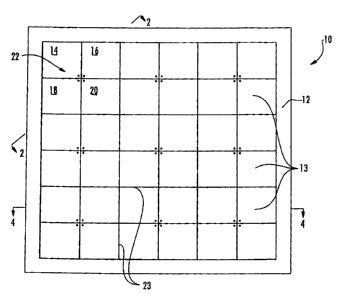
FIG. 1 is a schematic plan view of a dual-
polarization, slot-mode antenna array in accordance with the
present invention.
FIG. 2 is a cross-sectional view of the antenna
including the antenna feed structure taken along the line 2--2
in FIG. 1.
FIG. 3 is a perspective view of the feed line
organizer body of the antenna feed structure of FIG. 2.
FIG. 4 is a cross-sectional view of the ground
plane, dielectric layer, antenna units and upper dielectric
layer of the antenna taken along the line 4-4 in FIG. 1.
FIGs. 5A and SB are enlarged views of respective
embodiments of interdigitated spaced apart edge portions of
adjacent antenna elements of adjacent antenna units in the
antenna array of FIG. 1.
FIG. 6 is a schematic plan view of another
embodiment of the dual-polarization, slot-mode antenna array
in accordance with the present invention.
FIG. 7A is a cross-sectional view of the ground
plane, dielectric layer, antenna units, capacitive coupling
plates and upper dielectric layer of the antenna taken along
the line 7-7 in FIG. 6.
-5-
CA 02570652 2006-12-05
FIG. 7B is a cross-sectional view of another
embodiment with the capacitive coupling plates in the upper
dielectric layer of the antenna of FIG. 6.
The present invention will now be described more
fully hereinafter with reference to the accompanying drawings,
in which preferred embodiments of the invention are shown.
This invention may, however, be embodied in many different
forms and should not be construed as limited to the
embodiments set forth herein. Rather, these embodiments are
provided so that this disclosure will be thorough and
complete, and will fully convey the scope of the invention to
those skilled in the art. Like numbers refer to like elements
throughout, and prime notation is used to indicate similar
elements in alternative embodiments.
Referring to FIGS. 1-4, a dual polarization, slot-
mode antenna 10 according to the invention will now be
described. The antenna 10 includes a substrate 12 having a
ground plane 26 and a dielectric layer 24 adjacent thereto,
and at least one antenna unit 13 carried by the substrate.
Preferably, a plurality of antenna units 13 are arranged in an
array. As shown in FIG. 1, the antenna 10, for example,
includes nine antenna units 13. Each antenna unit 13 includes
four adjacent antenna patches or elements 14, 16, 18, 20
arranged in spaced apart relation from one another about a
central feed position 22 on the dielectric layer 24 opposite
the ground plane 26. Preferably, pairs of antenna elements,
e.g. 14/16 and 14/18, are fed with 0/180 phase across their
respective gaps to excite a slot mode. The phasing of the
element excitations also provides dual polarization, as would
be appreciated by the skilled artisan.
Each antenna unit may also include an antenna feed
structure 30 including four coaxial feed lines 32. Each
coaxial feed line 32 has an inner conductor 42 and a tubular
outer conductor 44 in surrounding relation thereto, for
-6-
CA 02570652 2006-12-05
example (FIG. 2). The antenna feed structure 30 includes a
feed line organizer body 60 having passageways 61 therein for
receiving respective coaxial feed lines 32. The feed line
organizer 60 is preferably integrally formed as a monolithic
unit, as will be appreciated by those of skill in the art.
More specifically, the feed line organizer body 60
may include a base 62 connected to the ground plane 26 and a
guide portion 63 carried by the base. The base 62 may have
holes 68 therein so that the base may be connected to the
ground plane 26 using screws. Of course, other suitable
connectors known to those of skill in the art may also be
used.
The guide portion 63 may include a bottom enclosed
guide portion 64 carried by the base 62, a top enclosed guide
portion 65 adjacent the antenna elements 14, 16, 18, 20, and
an intermediate open guide portion 66 extending between the
bottom enclosed guide portion and the top enclosed guide
portion. The outer conductor 44 of each coaxial feed line 32
may be connected to the feed line organizer body 60 at the
intermediate open guide portion 66 via solder 67, as
illustratively shown in FIG. 2.
The feed line organizer body 60 is preferably made
from a conductive material, such as brass, for example, which
allows for relatively easy production and machining thereof.
As a result, the antenna feed structure 30 may be produced in
large quantities to provide consistent and reliable ground
plane 26 connection. Of course, other suitable materials may
also be used for the feed line organizer body 60, as will be
appreciated by those of skill in the art.
Additionally, as illustratively shown in FIG. 3, the
passageways 61 are preferably parallel to a common axis A-A so
that the coaxial feed lines 32 are parallel and adjacent to
one another. Furthermore, the antenna feed structure 30 may
advantageously include a tuning plate 69 carried by the top
-7-
CA 02570652 2006-12-05
enclosed guide portion 65. The tuning plate 69 may be used to
compensate for feed inductance, as will be appreciated by
those of skill in the art.
More specifically, the feed line organizer body 60
allows the antenna feed structure 30 to essentially be
"plugged in" to the substrate 12 for relatively easy
connection to the at least one antenna unit 13. The antenna
feed structure 30 including the feed line organizer body 60
also allows for relatively easy removal and/or replacement
without damage to the antenna 10. Moreover, common mode
currents, which may result from improper grounding of the
coaxial feed lines 32 may be substantially reduced using the
antenna feed structure 30 including the feed line organizer
body 60. That is, the intermediate open guide portion 66
thereof allows for consistent and reliable grounding of the
coaxial feed lines 32.
The ground plane 26 may extend laterally outwardly
beyond a periphery of the antenna units 13, and the coaxial
feed lines 32 may diverge outwardly from contact with one
another upstream from the central feed position 22, as can be
seen in FIG. 2. The antenna 10 may also include at least one
hybrid circuit 50 carried by the substrate 12 and connected to
the antenna feed structure 30. The hybrid circuit 50
controls, receives and generates the signals to respective
antenna elements 14, 16, 18, 20 of the antenna units 13, as
would be appreciated by those skilled in the art.
The dielectric layer 24 preferably has a thickness
in a range of about 1/2 an operating wavelength near the top
of the operating frequency band of the antenna 10, and at
least one upper or impedance matching dielectric layer 28 may
be provided over the antenna units 13. This impedance
matching dielectric layer 28 may also extend laterally
outwardly beyond a periphery of the antenna units 13, as shown
in FIG. 4. The use of the extended substrate 12 and extended
-8-
CA 02570652 2006-12-05
impedance matching dielectric layer 28 result in an antenna
bandwidth of 2:1 or greater. The substrate 12 is flexible and
can be conformally mounted to a rigid surface, such as the
nose-cone of an aircraft or spacecraft, for example.
Referring more specifically to FIGs. 1, 5A and 5R,
adjacent patch antenna elements 14, 16, 18, 20 of adjacent
dual-polarization, slot-mode antenna units 13 include
respective spaced apart edge portions 23 having predetermined
shapes and relative positioning to provide increased
capacitive coupling therebetween. The respective spaced apart
edge portions 23 may be interdigitated, as shown in the
enlarged views of FIGs. 5A and 5B, to provide the increased
capacitive coupling therebetween. As such, the spaced apart
edge portions 23 may be continuously interdigitated along the
edge portions (FIG. 5A) or periodically interdigitated along
the edge portions (FIG. 5B).
Thus, an antenna array 10 with a wide frequency
bandwidth and a wide scan angle is obtained by utilizing the
antenna elements 14, 16, 18, 20 of each slot-mode antenna unit
13 having mutual capacitive coupling with the antenna elements
14, 16, 18, 20 of an adjacent slot-mode antenna unit 13.
Conventional approaches have sought to reduce mutual coupling
between elements, but the present invention makes use of, and
increases, mutual coupling between the closely spaced antenna
elements to achieve the wide bandwidth.
A related method aspect of the invention is for
making a dual-polarization, slot-mode antenna 10 including
forming an array of dual-polarization, slot-mode, antenna
units 13 carried by a substrate 12, each dual-polarization,
slot-mode antenna unit comprising four patch antenna elements
14, 16, 18, 20 arranged in laterally spaced apart relation
about a central feed position 22. The method includes shaping
and positioning respective spaced apart edge portions 23 of
adjacent patch antenna elements of adjacent dual-polarization,
-9-
CA 02570652 2006-12-05
slot-mode antenna units 13 to provide increased capacitive
coupling therebetween.
Shaping and positioning may include continuously or
periodically interdigitating the respective spaced apart edge
portions 23, as shown in the enlarged view of FIG. 5. Again,
the substrate 12 may be flexible and comprise a ground plane
26 and a dielectric layer 24 adjacent thereto, and forming the
array comprises arranging the four patch antenna elements 14,
16, 18, 20 on the dielectric layer opposite the ground plane
to define respective slots therebetween.
The method may further include forming an antenna
feed structure 30 for each antenna unit and comprising four
coaxial feed lines 32, each coaxial feed line comprising an
inner conductor 42 and a tubular outer conductor 44 in
surrounding relation thereto. The outer conductors 44 are
connected to the ground plane 26, and the inner conductors 42
extend outwardly from ends of respective outer conductors,
through the dielectric layer 24 and are connected to
respective patch antenna elements adjacent the central feed
position 22, for example, as shown in FIG. 2.
Referring now to FIGs. 6, 7A and 7B, another
embodiment of a dual-polarization, slot mode antenna 10' will
now be described. Adjacent patch antenna elements 14, 16, 18,
20 of adjacent dual-polarization, slot-mode antenna units 13'
have respective spaced apart edge portions 23 defining gaps
therebetween. A capacitive coupling layer or plates 70 are
adjacent the gaps and overlap the respective spaced apart edge
portions 23 to provide the increased capacitive coupling
therebetween. The capacitive coupling layer or plates 70 may
be arranged within the dielectric layer 24 (FIG. 7A) below the
patch antenna elements or within the second dielectric layer
28 above the patch antenna elements plane.
Thus, an antenna array 10' with a wide frequency
bandwidth and a wide scan angle is obtained by utilizing the
-10-
CA 02570652 2006-12-05
antenna elements 14, 16, 18, 20 of each slot-mode antenna unit
13 having mutual capacitive coupling with the antenna elemerits
14, 16, 18, 20 of an adjacent slot-mode antenna unit 13'.
A method aspect of this embodiment of the invention
is directed to making a dual-polarization, slot-mode antenna
and includes providing a respective capacitive coupling plat:e
70 adjacent each gap and overlapping the respective spaced
apart edge portions 23 to provide the increased capacitive
coupling therebetween. Again, the capacitive coupling plates
70 may be arranged within the dielectric layer 24 below the
patch antenna elements or within the second dielectric layer
28 above the patch antenna elements.
The antenna 10, 10' may have a seven-to-one
bandwidth for 2:1 VSWR, and may achieve a scan angle of +/- 75
degrees. The antenna 10, 10' may have a greater than ten-to-
one bandwidth for 3:1 VSWR. Thus, a lightweight patch array
antenna 10, 10' according to the invention with a wide
frequency bandwidth and a wide scan angle is provided. Also,
the antenna 10, 10' is flexible and can be conformally
mountable to a surface, such as an aircraft.
-11-