Note: Descriptions are shown in the official language in which they were submitted.
CA 02570880 2006-12-08
179845-2 (RD)
METHOD OF MAKING AN ELECTRONIC DEVICE COOLING SYSTEM
BACKGROUND
The invention relates generally to a cooling system for electronic devices,
and in
particular to processes for fabricating microchannels for circulating a fluid
in a device
cooling system.
The development of high density power electronics has made it increasingly
more
difficult to fabricate efficient cooling systems. With modern silicon based
power
devices capable of dissipating heat up to 500 W/cm2, there is a need for
improved
thermal management solutions. Natural and forced-air cooling schemes can only
handle heat fluxes of up to about 1 W/cm2. Conventional liquid cooling plates
can
achieve heat fluxes of the order of 20 W/cm2. However, microchannel cooling
technology has demonstrated the ability to greatly enhance cooling
performance, on
the order of about 1000 W/cm2.
In certain proposed structures, microchannels are fabricated on the reverse
side of
power devices through which a coolant fluid is circulated to dissipate heat
generated
by the device. The efficiency of cooling depends on the width and the
uniformity of
the channels. Within certain limits, for example, narrower channels tend to
dissipate
heat better due to better contact with the coolant fluid. However, the
increased heat
transfer in narrower channels may often be offset by increased pressure losses
across
the channel, which may result in challenges in forcing cooling fluid through
the
system. Another limitation may be the non-uniformity of the microchannels,
which
may result in hot spots that may adversely affect the perfoimance of the power
device
and may even result in break-down of the devices. Silicon is the commonly used
material for microchannel fabrication. However, channels made of material
having
higher thermal conductivity than silicon may show better efficiency due to
their better
heat transfer properties.
1
CA 02570880 2006-12-08
179845-2 (RD)
Moreover, while such structures have been proposed and tested, efficient and
economical method for their manufacture is still lacking. The stringent
requirements
of reliably creating uniform microchannels have simply not been addressed
adequately in the art.
Therefore, there is a need for improving the current techniques for
fabricating
microchannels with narrower channel width and better uniformity. There is, in
particular, a need for fabricating such devices in an efficient, low-cost
manner.
BRIEF DESCRIPTION
Embodiments of the present invention address this and other needs. In one
embodiment, a method of making an electronic device cooling system includes
forming a thermally conductive layer on an inner surface of the substrate and
laser
ablating the thermally conductive layer to form microchannels.
DRAWINGS
These and other features, aspects, and advantages of the present invention
will
become better understood when the following detailed description is read with
reference to the accompanying drawings in which like characters represent like
parts
throughout the drawings,
FIG. 1 illustrates an exemplary cooling system for a power device fabricated
in
accordance with aspects of the present invention;
FIG. 2 is an exploded view of the cooling system with the power device shown
in
FIG. 1;
FIGS. 3-9 illustrate fabrication stages of microchannels for a device of the
type shown
in FIGS. 1 and 2 in accordance with a plating technique;
FIGS. 10-12 illustrate fabrication stages of microchannels in accordance with
a
variant of the embodiment of FIGS. 3-9;
2
CA 02570880 2006-12-08
179845-2 (RD)
FIG. 13 is a flow chart depicting a method of fabricating microchannels in
accordance
with the embodiment of FIGS. 3-9;
FIGS. 14-20 illustrate fabrication stages of microchannels in accordance with
the
embodiment of FIGS. 10-12;
FIG. 21 is a flow chart of a method of fabricating microchannels in accordance
with
another variant of the method;
FIGS. 22-26 illustrate fabrication stages of microchannel formation according
to a
laser ablation technique; and
FIG. 27 is a flow chart of a method of fabricating microchannels in accordance
with
the embodiment of FIGS. 22-26.
DETAILED DESCRIPTION
FIG. 1 is a schematic representation of an electronic circuit assembly 10 for
a device,
such as a power electronic device. The circuit assembly 10 includes a
substrate 12.
The substrate 12 may comprise semiconductors commonly used in power electronic
devices, such as silicon, silicon carbide, alumina, aluminum nitride, gallium
nitride or
a combination thereof. The devices 14 are mounted proximate to a surface of
the
substrate 12, as shown in FIG. 1. The figure depicts six such devices mounted
on the
substrate 12. As will be appreciated by one skilled in the art, any number of
devices
or even a single device may be mounted on the substrate. Similarly, any
desired
devices may be mounted on the substrate, particularly devices that generate
significant heat during operation that requires extraction or dissipation.
Such devices
may include, for example, solid state switching devices.
Further, the system 10 includes a conductive layer 16 disposed on the opposite
surface
of the substrate 12. The conductive layer 16 may comprise any suitable
thermally
conducting material, such as copper. The conductive layer may act as a heat
dissipation interface between the device 14 and cooling system due to its
enhanced
heat transfer properties.
3
CA 02570880 2006-12-08
179845-2 (RD)
A heat exchange layer 18 is placed on the conductive layer 16. The heat
exchange
layer 18 includes microchannels 22 for flowing a coolant. Suitable coolants
include
oil, water, ethylene glycol, aircraft fuel or a combination thereof. It should
be noted that
a liquid or gaseous coolant may be used, and the invention is not intended to
be limited
to either, or to any particular cooling medium. A manifold 20 is attached to
the heat
exchange layer 18. The manifold 20 further includes an inlet plenum 24 for
directing
the coolant to the microchannels, and an outlet plenum 26 to exhaust the
coolant from
the microchannels. The details of the manifold structure are shown in FIG. 2.
FIG. 2 is an exploded view of the circuit assembly 10 illustrated in FIG. 1. A
surface
of the substrate 12, on which the device 14 is mounted is represented as an
outer
surface 28, and the opposite side on which the conductive layer 16 is formed
is
represented as an inner surface 30. The heat exchange layer 18 is disposed on
the
conductive layer 16 and microchannels 22 are formed in the heat exchange layer
18.
The microchannels 22 extend from the conductive layer 16 to the manifold 20.
The
manifold 20 have two sets of channels 32 and 34 formed on a surface facing the
microchannels 22. The inlet plenum 24 introduces a coolant to the
microchannels 22
through the set of channels 32, otherwise referred to as inlet manifolds. The
outlet
plenum 26 exhausts the coolant from the microchannels 22 through the set of
channels
34, and these channels are referred to as outlet manifolds. The fabrication of
the
microchannels 22 will be discussed below.
FIGS 3-9 illustrate fabrication stages of microchannels 22 in accordance with
one
embodiment. The substrate 12 having the inner surface 30 is provided as shown
in
FIG. 3. The substrate 12 may be a semiconductor and in this instance is made
of
silicon carbide. The conductive layer 16 is disposed on the substrate 12. The
conductive layer may be formed using deposition techniques such as
electroplating.
In this embodiment, a thickness of the conductive layer is less than about 300
microns. Further, the conductive layer 16 is made of a material having good
thermal
conductivity such as copper. Other materials that can be used include gold and
silver.
A sacrificial layer 36 is then disposed on the conductive layer 16 as shown in
FIG. 4.
In this example, sacrificial layer 36 is made of silicon, although other
materials may
4
CA 02570880 2006-12-08
179845-2 (RD)
be used. In the illustrated embodiment, the thickness of the sacrificial layer
36
formed is less than about 400 microns. It should be noted that the thickness
of the
sacrificial layer 36 may vary depending on depth of microchannels desired.
FIG. 5 depicts channel formation in the sacrificial layer 36 of FIG. 4. In the
illustrated embodiment, grooves are represented by reference numeral 38, and
reference numera140 represents ribs of the channel. The formation of the
channels is
through etching the sacrificial layer 36 using an etchant. For example,
potassium
hydroxide solution is an etchant for a sacrificial layer made of silicon.
Potassium
hydroxide preferentially etches silicon while the underlying conductive layer
16 is not
affected. Prior to etching, in one example, regions that may form ribs may be
masked
and then potassium hydroxide solution is used to remove regions of silicon
exposed to
the potassium hydroxide solution. Further, the exposure to the potassium
hydroxide
solution is continued until the conductive layer 16 is reached. Vertical
channels as
depicted in figures may be formed. The grooves 38 of the channel may have a
depth
related to the thickness of the sacrificial layer 36 formed. In a present
embodiment,
the grooves 38 may have a depth of less than about 400 microns. In a
particular
example, the grooves 38 may have a depth of from about 300 microns to about
400
microns. The formation of channels results in a rib 40 having a width of less
than
about 200 microns. In a specific embodiment, the ribs 40 have a width of about
100
microns to about 200 microns. As will be appreciated by those skilled in the
art, the
rib width may depend on inherent limitations of etching techniques, for
example
limitations of the mask used.
Following channel formation in the sacrificial layer, plating is carried out
as shown in
FIG. 6. The plating may be through electroplating, in one example. The plating
substantially covers the channels and forms an upper layer 46 of plating
material as
shown. In this embodiment, the plating material comprises a thermally
conducting
material, such as copper, silver, gold or an alloy of these. In the
illustrated example
copper has been used.
The upper layer 46 of the plating material formed above the rib 40 of the
channel is
removed to expose the sacrificial layer 36, as shown in FIG. 7. The plating
material
CA 02570880 2006-12-08
179845-2 (RD)
may be removed by grinding. The grinding is carried out so that a top surface
of the
plating material and the rib 40 are on a same plane to expose the sacrificial
layer 36.
FIG. 8 illustrates microchannel formation in the sacrificial layer 36. The
exposed
sacrificial layer 36 made of silicon is etched using a solution of potassium
hydroxide.
The potassium hydroxide solution etches silicon while the copper used for
plating,
and which forms conductive ribs 44, remains. A region between the conductive
ribs,
previously of silicon, forms the microchannels 22. The microchannels may be
defined in terms of an aspect ratio of width to height of the microchannels
22. For a
cooling system, it is desirable to have as high an aspect ratio as possible.
The width
of the microchannels 22 follows the width of the rib 40 and is less than about
200
microns. In a specific embodiment, the microchannels have a width from about
100
microns to about 200 microns. The microchannels may be about 400 microns deep.
In particular embodiments, the depth of the microchannel may vary from about
300
microns to about 400 microns. Based on the width and height of the
microchannels,
the aspect ratio of the microchannels is in a range from about 1:2 to about
1:3.
FIG. 9 shows the addition of the manifold 20 and the devices 14 on the cooling
system. Subsequent to microchannel formation, the manifold 20 is attached to
the
thermally conductive ribs 44 between which the microchannels are formed.
Further,
the devices that have been attached on an outer surface of the substrate 12
are
represented by reference numeral 14. In practice, a single device or a
plurality of
devices may be mounted on the substrate as shown. It should be noted that,
where
desired, and depending upon the particular processing used, the devices may
actually
be mounted prior to formation of the microchannels.
FIGS. 10-12 depict a variation on the fabrication steps of the microchannels
with an
additional conductive layer. FIG. 10 depicts the substrate 12 over which the
conductive layer 16 is formed. The substrate is again a semiconductor
material. The
conductive layer 16 is formed by deposition, using a sputtering technique, on
the
substrate 12. The sputtering results in a thickness of about 1 micron in a
present
embodiment. The conductive layer 16 is made of a material with good thermal
conductivity, such as copper. A second conductive layer 48, such as copper,
may be
6
CA 02570880 2006-12-08
179845-2 (RD)
deposited over the layer 16 as shown in FIG 11, and secured to the underlying
layer
by direct bonding between the materials constituting these layers. The second
conductive layer 48 may be plated over the first conductive layer 16. FIG. 12
shows
the formation of the sacrificial layer 36 on the second conductive layer 48.
Typical
thickness of the sacrificial layer 36 formed is less than about 400 microns.
The
thickness of the layer 36 may vary depending on depth of microchannels 22
desired.
Fabrication stages as discussed with reference to FIGS 5-8 may then be
followed to
form the microchannels in the sacrificial layer 36.
The method of forming microchannels 22 illustrated above is summarized using a
flow chart 50 of FIG. 13. At step 52 of the FIG. 13, a conductive layer is
deposited on
the inner surface of the substrate. Again, the conductive layer is deposited
through a
sputtering technique or by electroplating. Optionally, a second conductive
layer may
be added over the conductive layer, as represented by step 54. The sacrificial
layer is
then deposited on the conductive layer at step 56. At step 58, the sacrificial
layer is
etched to the conductive layer to form channels. The etched sacrificial layer
is then
plated in step 60 to substantially fill the channels as illustrated in FIG. 6.
Further, the
thin surface of the plating material is removed at step 62 to expose the
surface of the
sacrificial layer, such as by grinding. The remaining sacrificial layer is
then etched in
step 64 to form microchannels. A selective etchant discussed with reference to
step
58 may be used. The etchant removes the sacrificial layer while the plating
material
remains unetched. Regions of etched sacrificial layer forms the microchannels
separated by heat exchanging ribs. In step 66, the manifold and devices are
added.
Subsequent to microchannel formation devices are mounted on the substrate, and
the
manifold is attached on a surface facing the microchannels.
In accordance with yet another plating embodiment, a method of forming
microchannels is provided as shown in FIGS. 14-20. In the illustrated
embodiment,
the conductive layer 16 is formed on the substrate 12 as shown in FIG. 14. The
conductive layer is formed using deposition techniques known to those skilled
in the
art, such as sputtering. Typical thickness of the conductive layer 16 is less
than about
300 microns, although this may vary. Suitable substrates again include
7
CA 02570880 2006-12-08
179845-2 (RD)
semiconductors used in power electronic devices such as Si, SiC, Alumina, AIN,
GaN, or a combination of these. As before, the conductive layer 16 is made of
a
conducting material such as Cu, Ag, Au, or any combinations thereof, or any
other
suitable material.
As illustrated in FIG. 15, the sacrificial layer 36 is formed on the
conductive layer 16
with the help of an adhesive layer 68. The adhesive layer 68 is sandwiched
between
the layers 16 and 36 and promotes bonding between the adhesive layer 68 and
the
conductive layer 16, and also between the adhesive layer 68 and the
sacrificial layer
36. Typical thickness of the adhesive layer 68 may be about 12 microns to
about 14
microns. Suitable adhesive material includes a thermosetting material, a
thermoplastic material or an epoxy. In this example, the sacrificial layer 36
is made
of silicon, although other materials may be used. Typical thickness of the
sacrificial
layer 36 is less than about 400 microns. The thickness of the layer 36 may
vary
depending on depth of microchannels desired.
FIG. 16 illustrates formation of channels in the sacrificial layer 36.
Elements 40 are
ribs, and channels 38 in sacrificial layer 36 and the adhesive layer 68, and
are formed
by sawing to the conductive layer 16 to form the ribs 40. It has been found
that
silicon having 110 orientation plane, on sawing form good vertical channels.
Further,
any sawing method known in the art may be used. In one example, a thermocarbon
blade is used and parameters of sawing are adjusted to form channels of about
100
microns wide. The grooves 38 may have a depth of less than about 400 microns.
In
particular examples, the grooves 38 may have a depth of from about 300 microns
to
about 400 microns. The formation of channels results in ribs 40 having a width
of
less than about 200 microns in a present embodiment. In a specific embodiment,
the
ribs 40 have a width of about 100 microns to about 200 microns.
In FIG 17, a plating material is added on the sacrificial layer 16 to
substantially fill the
grooves 38 and form the surface 46 of the plating material, as in the
embodiment
described above. Next, as illustrated in FIG. 18, the plating material is
ground to
expose the sacrificial layer 36. The grinding results in a top surface of the
sacrificial
layer 36 and the plating material being on a same plane.
8
CA 02570880 2006-12-08
179845-2 (RD)
Following grinding, the exposed sacrificial layer 36 is etched to the adhesive
layer 68,
as shown in FIG. 19. The etching is carried out through an etchant that
preferentially
etches the sacrificial layer remaining between the ribs. Alternatively, a
method of
masking with subsequent etching may be used, such that a region exposed to
etchant
is removed. A potassium hydroxide solution is an acceptable etchant for a
sacrificial
layer made of silicon. Potassium hydroxide preferentially etches silicon while
the
underlying adhesive layer 68 is not affected. The exposure to the potassium
hydroxide solution is continued until the adhesive layer 68 is reached. The
adhesive
layer 68 is then etched to expose the conductive layer 16, as shown in FIG.
20.
Again, an etchant which etches the adhesive layer while the conductive layer
16
remains unetched, is used. The etching results in formation of the conductive
ribs 44.
A region between the conductive ribs 44, previously of silicon and adhesive,
form the
microchannels 22. The resulting dimensions of the ribs and microchannels may
be
similar to those described above for the first embodiment.
FIG. 21 is a flow chart 70, illustrating the method employing sawing to form
microchannels prior to plating. At step 72, a conductive layer is deposited on
the
substrate.
A sacrificial layer is then adhered to the conductive layer by means of an
adhesive
layer, as represented by step 74. At step 76, channels are formed in the
sacrificial
layer by sawing. Sawing may result in debris formation at the edges of the
sacrificial
layer, which is removed during cleaning. It should be noted that the channel
shape
resulting from sawing may depend on the material used. In one example, as
noted
above, silicon having an orientation of 110 is used as the sacrificial layer
which on
sawing results in a vertical channel. Following sawing to form channels, a
plating
material is deposited on the sawed sacrificial layer at step 78. The surface
formed as a
result of plating is removed at step 80 to expose the sacrificial layer. At
step 82, the
exposed sacrificial layer is etched, and at step 84, the adhesive layer is
removed by
etching to form microchannels. Following channel formation, manifold and
devices
are added, at step 86, to form a device cooling system.
9
CA 02570880 2006-12-08
179845-2 (RD)
In accordance with another embodiment, microchannels are formed through laser
ablation of a substrate having an inner surface and an outer surface. A
copper, or any
such conducting material is disposed on the inner surface of the substrate to
form a
thermally conductive layer, and microchannels are formed in the copper layer
by
successive ablation of progressively deeper channels in the conductive layer.
FIGS 22-26 illustrate fabrication stages of microchannel formation by laser
ablation.
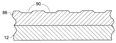
As illustrated in FIG. 22, a copper layer 88 is formed on the substrate 12.
The
substrate 12 is a semiconductor material commonly used in power electronic
devices,
such as one of the materials described above. The copper layer 88 is deposited
on the
substrate 12 through an electroplating process, in one example. Other
techniques
known to those skilled in the art may be used. The electroplating results in a
copper
layer 88 having a thickness of about 400 microns in a present example,
although other
thicknesses may be used.
The copper layer 88 is laser ablated, as shown in FIG. 23, to form partially
ablated
channels 90. In one example, between successive laser ablation steps, a
silicone mold
release agent, or other cleaning medium is applied on the copper layer 88. It
has been
found that the ablation process may result in debris within the progressively
formed
microchannels that may reattach to the walls of the microchannels. The
application of
the cleaning agent between ablation steps effectively removes this debris, or
at least
prevents it from reattaching to the microchannel wall. The copper layer is
then
subjected to laser ablation and again is sprayed with silicone mold release
agent.
After each application of the cleaning agent, the surface is wiped to remove
debris
formed as a result of laser ablation. In another example, the substrate is
flushed with
water between successive laser ablation passes to remove the debris formed.
Alternatively, a chemical etch clean-up may be used. In such cases, a chemical
etch
stop may be applied on the copper layer 88. The copper layer 88 is then
subjected to
laser ablation. Following laser ablation, a ferric chloride solution is
disposed on the
copper layer and debris resulting from ablation is rinsed off to form
partially ablated
channels 90. The ablate and etch process may be done in successive passes
until the
desired depth is achieved.
CA 02570880 2006-12-08
179845-2 (RD)
Optionally, the laser ablation may be carried out under water using techniques
known
to one skilled in the art, for example the laser beam passes through water and
ablates
the substrate. Advantageously, this may result in clearing debris formed as a
result of
successive laser passes and may result in faster laser ablation rate but a
higher laser
power may be required.
FIG. 24 shows a partially ablated channel 90 having deeper channels than those
shown in FIG. 23. The silicone mold release agent is again applied on the
copper
layer and is followed by laser ablation and the debris is wiped off to form
deeper
channels 90. Similarly, when a chemical etch stop is applied on the copper
layer the
debris that forms is rinsed off after applying a ferric chloride solution. The
steps
discussed with reference to FIG. 24 are repeated to progressively form the
microchannels to a desired depth, as shown in FIG. 25. The microchannels 22
resulting through laser ablation are typically V-shaped. Typical thickness of
the
microchannels is less than about 200 microns in a present embodiment. In
specific
embodiments, the thickness may vary from about 100 microns to about 200
microns.
The microchannels may be less than about 400 microns deep. In particular
embodiments, the depth of the microchannels may vary from about 300 microns to
about 400 microns. Following microchannel formation, the silicone release
agent or
other chemicals used during the ablation may be removed. In one example, 50
percent by volume of limonene and propanol solution is used to remove the
adhering
silicone release agent. Additionally, even nitrogen gas may be used to blow
off the
debris.
As illustrated in FIG. 26, the manifold 20 and the device 14 are then added. A
surface
of the manifold 20 includes an inlet manifold in fluid communication with the
microchannels and operable to introduce a coolant to the microchannels 22, and
an
outlet manifold in fluid communication with the microchannels 22 and operable
to
exhaust the coolant from the microchannels 22, as in the previous embodiments.
The
devices 14 are mounted proximate to the outer surface of the substrate 12. As
mentioned above, in certain applications, the devices may be mounted prior to
laser
ablation and addition of the manifolds.
11
CA 02570880 2006-12-08
179845-2 (RD)
The fabrication method of FIGS. 22-26 is summarized in flow chart 92 of FIG.
27. At
step 96, the thermally conductive layer is subjected to laser ablation. The
laser
parameters, such as time of exposure, power of the laser is measured and
standardized
before exposing the thermally conductive layer, and will typically depend upon
the
nature and design of the laser, the material used for the conductive layer,
and the
desired depth of the microchannels. At step 98, following laser ablation, the
silicone
release agent is applied on the thermally conductive layer and the layer is
wiped to
remove debris. Steps 96 and 98 are repeated a number of times until the
desired
channel dimension is obtained. In one example, the steps 96 and 98 were
repeated a
sufficient number of times to obtain a channel depth of about 100 microns.
Laser
ablation results in a V-shaped channel. After the microchannel formation a
clean-up
is carried out. The clean-up includes a combination of scrubbing, applying a
solvent
or blowing a gas. At step 102, a manifold, and devices are mounted on the
processed
substrate and thermally conductive layer.
While only certain features of the invention have been illustrated and
described
herein, many modifications and changes will occur to those skilled in the art.
It is,
therefore, to be understood that the appended claims are intended to cover all
such
modifications and changes as fall within the true spirit of the invention.
12