Note: Descriptions are shown in the official language in which they were submitted.
CA 02570898 2007-10-02
Method and System For Driving An Active Matrix Display Circuit
CROSS-REFERENCE TO RELATED APPLICATION(S)
[0001] This application claims priority to Canadian Patent Application Ser.
No. 2,535, 233,
filed on January 9, 2006, and Canadian Patent Application Ser. No. 2,551,237,
filed on June 27,
2006.
FIELD OF INVENTION
[0002] The invention relates to a light emitting device, and more specifically
to a method and
system for driving a pixel circuit having a light emitting device.
BACKGROUND OF THE INVENTION
[0003] Electro-luminance displays have been developed for a wide variety of
devices, such as
cell phones. In particular, active-matrix organic light emitting diode
(AMOLED) displays with
amorphous silicon (a-Si), poly-silicon, organic, or other driving backplane
have become more
attractive due to advantages, such as feasible flexible displays, its low cost
fabrication, high
resolution, and a wide viewing angle.
[0004] An AMOLED display includes an array of rows and columns of pixels, each
having an
organic light emitting diode (OLED) and backplane electronics arranged in the
array of rows
and columns. Since the OLED is a current driven device, the pixel circuit of
the AMOLED
should be capable of providing an accurate and constant drive current.
[0005] There is a need to provide a method and system that is capable of
providing constant
brightness with high accuracy and reducing the effect of the aging of the
pixel circuit and the
instability of backplane and a light emitting device.
SUMMARY OF THE INVENTION
[0006] It is an object of the invention to provide a method and system that
obviates or mitigates
at least one of the disadvantages of existing systems.
CA 02570898 2007-01-05
[0007] In accordance with an aspect of the present invention there is provided
a system a
display system, including a drive circuit for a pixel having a light emitting
device. The drive
circuit includes a drive transistor connected to the light emitting device.
The drive transistor
includes a gate terminal, a first terminal and a second terminal. The drive
circuit includes a first
transistor including a gate terminal, a first terminal and a second terminal,
the gate terminal of
the first transistor being connected to a select line, the first terminal of
the first transistor being
connected to a data line, the second terminal of the first transistor being
connected to the gate
terminal of the drive transistor. The drive circuit includes a circuit for
adjusting the gate
voltage of the drive transistor, the circuit including a discharging
transistor having a gate
terminal, a first terminal and a second terminal, the gate terminal of the
discharging transistor
being connected to the gate terminal of the drive transistor at a node, the
voltage of the node
being discharged through the discharging transistor. The drive circuit
includes a storage
capacitor including a first terminal and a second terminal, the first terminal
of the storage
capacitor being connected to the gate terminal of the drive transistor at the
node.
[0008] The display system may include a display array having a plurality of
pixel circuits
arranged in rows and columns, each of the pixel circuits including the drive
circuit, and a driver
for driving the display array. The gate terminal of the second transistor is
connected to a bias
line. The bias line may be shared by more than one pixel circuit of the
plurality of pixel circuits.
[0009] In accordance with a further aspect of the present invention there is
provided a method
for the display system. The display system includes a driver for providing a
programming
cycle, a compensation cycle and a driving cycle for each row. The method
includes the steps of
at the programming cycle for a first row, selecting the address line for the
first row and
providing programming data to the first row, at the compensation cycle for the
first row,
selecting the adjacent address line for a second row adjacent to the first row
and disenabling the
address line for the first row, and at the driving cycle for the first row,
disenabling the adjacent
address line.
[0010] In accordance with a further aspect of the present invention there is
provided a display
system, including one or more than one pixel circuit, each including a light
emitting device and
-2-
CA 02570898 2007-01-05
a drive circuit. The drive circuit includes a drive transistor including a
gate terminal, a first
terminal and a second terminal, the drive transistor being between the light
emitting device and
a first power supply. The drive circuit includes a switch transistor including
a gate terminal, a
first terminal and a second terminal, the gate terminal of the switch
transistor being connected
to a first address line, the first terminal of the switch transistor being
connected to a data line,
the second terminal of the switch transistor being connected to the gate
terminal of the drive
transistor. The drive circuit includes a circuit for adjusting the gate
voltage of the drive
transistor, the circuit including a sensor for sensing energy transfer from
the pixel circuit and a
discharging transistor, the sensor having a first terminal and a second
terminal, a property of the
sensor varying in dependence upon the sensing result, the discharging
transistor having a gate
terminal, a first terminal and a second terminal, the gate terminal of the
discharging transistor
being connected to a second address line, the first terminal of the
discharging transistor being
connected to the gate terminal of the drive transistor at a node, the second
terminal of the
discharging transistor being connected to the first terminal of the sensor.
The drive circuit
includes a storage capacitor including a first terminal and a second terminal,
the first terminal
of the storage capacitor being connected to the gate terminal of the drive
transistor at the node.
[0011] In accordance with a further aspect of the present invention there is
provided a method
for a display system, including the step of implementing an in-pixel
compensation.
[0012] In accordance with a further aspect of the present invention there is
provided a method
for a display system, including the step of implementing an of-panel
compensation.
[0013] In accordance with a further aspect of the present invention there is
provided a method
for a display system, which includes a pixel circuit having a sensor,
including the step of
reading back the aging of the sensor.
[0014] In accordance with a further aspect of the present invention there is
provided a display
system, including a display array including a plurality of pixel circuits
arranged in rows and
columns, each including a light emitting device and a drive circuit; and a
drive system for
driving the display array. The drive circuit includes a drive transistor
including a gate terminal,
-3-
CA 02570898 2007-01-05
a first terminal and a second terminal, the drive transistor being between the
light emitting
device and a first power supply. The drive circuit includes a first transistor
including a gate
terminal, a first terminal and a second terminal, the gate terminal of the
first transistor being
connected to an address line, the first terminal of the first transistor being
connected to a data
line, the second terminal of the first transistor being connected to the gate
terminal of the drive
transistor. The drive circuit includes a circuit for adjusting the gate
voltage of the drive
transistor, the circuit including a second transistor, the second transistor
having a gate terminal,
a first terminal and a second terminal, the gate terminal of the second
transistor being connected
to a control line, the first terminal of the second transistor being connected
to the gate terminal
of the drive transistor. The drive circuit includes a storage capacitor
including a first terminal
and a second terminal, the first terminal of the storage capacitor being
connected to the gate
terminal of the drive transistor. The drive system drives the pixel circuit so
that the pixel
circuit is turned off for a portion of a frame time.
[0015] In accordance with a further aspect of the present invention there is
provided a method
for a display system having a display array and a driver system. The drive
system provides a
frame time having a programming cycle, a discharge cycle, an emission cycle, a
reset cycle, and
a relaxation cycle, for each row. The method includes the steps of at the
programming cycle,
programming the pixel circuits on the row by activating the address line for
the row; at the
discharge cycle, partially discharging the voltage on the gate terminal of the
drive transistor by
deactivating the address line for the row and activating the control line for
the row; at the
emission cycle, deactivating the control line for the row, and controlling the
light emitting
device by the drive transistor; at the reset cycle, discharging the voltage on
the gate terminal of
the drive transistor by activating the control line for the row; and at the
relaxation cycle,
deactivating the control line for the row.
BRIEF DESCRIPTION OF THE DRAWINGS
[0016] These and other features of the invention will become more apparent
from the following
description in which reference is made to the appended drawings wherein:
-4-
CA 02570898 2007-01-05
Figure 1 is a diagram illustrating an example of a pixel circuit to which a
pixel drive scheme in
accordance with an embodiment of the present invention is applied;
Figure 2 is a diagram illustrating another example of a pixel circuit having a
drive circuit of
Figure 1;
Figure 3 is a timing diagram for an example of a method of driving a pixel
circuit in accordance
with an embodiment of the present invention;
Figure 4 is a diagram illustrating an example of a display system for the
drive circuit of Figures
l and 2;
Figure 5 is a diagram illustrating an example of a pixel circuit to which a
pixel drive scheme in
accordance with another embodiment of the present invention is applied;
Figure 6 is a diagram illustrating another example of a drive circuit of
Figure 5;
Figure 7 is a diagram illustrating a further example of the drive circuit of
Figure 5;
Figure 8 is a diagram illustrating another example of a pixel circuit having
the drive circuit of
Figure 5;
Figure 9 is a timing diagram for an example of a method of driving a pixel
circuit in accordance
with another embodiment of the present invention;
Figure 10 is a diagram illustrating an example of a display system for the
drive circuit of
Figures 5 and 8;
Figure 11 is a diagram illustrating an example of a display system for the
drive circuit of
Figures 6 and 7; ,
Figure 12 is a graph illustrating simulation results for the pixel circuit of
Figure 1;
Figure 13 is a diagram illustrating an example of a pixel circuit to which a
pixel drive scheme
in accordance with a further embodiment of the present invention is applied;
-5-
CA 02570898 2007-01-05
Figure 14 is a diagram illustrating another example of a pixel circuit having
a drive circuit of
Figure 13;
Figure 15 is a timing diagram for an example of a method of driving a pixel
circuit in
accordance with a further embodiment of the present invention;
Figure 16 is a diagram illustrating an example of a display system for the
drive circuit of
Figures 13 and 14;
Figure 17 is a graph illustrating simulation results for the pixel circuit of
Figure 5;
Figure 18 is a graph illustrating simulation results for the pixel circuit of
Figure 5;
Figure 19 is a timing diagram for the operation of the display system of
Figure 16.
Figure 20 is a diagram illustrating an example of a pixel circuit to which a
pixel drive scheme
in accordance with a further embodiment of the present invention is applied;
Figure 21 is a diagram illustrating anther example of a pixel circuit having
the drive circuit of
Figure 20;
Figure 22 is a timing diagram illustrating an example of a method of driving a
pixel circuit in
accordance with a further embodiment of the present invention;
Figure 23 is a diagram illustrating an example of a display system for the
drive circuit of
Figures 20 and 21;
Figure 24 is a diagram illustrating another example of a display system for
the drive circuit of
Figures 20 and 21;
Figure 25 is a diagram illustrating an example of a pixel system in accordance
with an
embodiment of the present invention;
Figure 26 is a diagram illustrating an example of a display system having a
read back circuit of
Figure 25;
-6-
CA 02570898 2007-01-05
Figure 27 is a diagram illustrating another example of a display system having
the read back
circuit of Figure 25;
Figure 28 is a timing diagram illustrating an example of a method of driving a
pixel circuit in
accordance with a further embodiment of the present invention;
Figure 29 is a diagram illustrating an example of a method of extracting the
aging of a sensor
of Figure 25;
Figure 30 is a diagram illustrating an example of a pixel system in accordance
with another
embodiment of the present invention;
Figure 31 is a diagram illustrating an example of a display system having a
read back circuit of
Figures 30;
Figure 32 is a diagram illustrating another example of a display system having
the read back
circuit of Figure 30;
Figure 33 is a timing diagram illustrating an example of a method of driving a
pixel circuit in
accordance with a further embodiment of the present invention;
Figure 34 is a timing diagram illustrating another example of a method of
extracting the aging
of a sensor of Figure 30;
Figure 35 is a diagram illustrating an example of a pixel circuit to which a
pixel drive scheme
in accordance with a further embodiment of the present invention is applied;
Figure 36 is a timing diagram for an example of a method of driving a pixel
circuit in
accordance with a further embodiment of the present invention;
Figure 37 is a diagram illustrating an example of a display system having the
pixel circuit of
Figure 35; and
-7-
CA 02570898 2007-01-05
Figure 38 is a diagram illustrating another example of a display system having
the pixel circuit
of Figure 35.
DETAILED DESCRIPTION
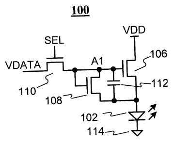
[0017] Figure 1 illustrates an example of a pixel circuit to which a pixel
drive scheme in
accordance with an embodiment of the present invention is applied. The pixel
circuit 100 of
Figure 1 includes an OLED 102 and a drive circuit 104 for driving the OLED
102. The drive
circuit 104 includes a drive transistor 106, a discharging transistor 108, a
switch transistor 110,
and a storage capacitor 112. The OLED 102 includes, for example, an anode
electrode, a
cathode electrode and an emission layer between the anode electrode and the
cathode electrode.
[0018] In the description below, "pixel circuit" and "pixel" are used
interchangeably. In the
description below, "signal" and "line" may be used interchangeably. In the
description below,
the terms "line" and "node" may be used interchangeably. In the description,
the terms "select
line" and "address line" may be used interchangeably. In the description
below, "connect (or
connected)"and "couple (or coupled)" may be used interchangeably, and may be
used to
indicate that two or more elements are directly or indirectly in physical or
electrical contact
with each other.
[0019] In one example, the transistors 106, 108 and 110 are n-type
transistors. In another
example, the transistors 106, 108 and 110 are p-type transistors or a
combination of n-type and
p-type transistors. In one example, each of the transistors 106, 108 and 110
includes a gate
terminal, a source terminal and a drain terminal.
[0020] The transistors 106, 108 and 110 may be fabricated using amorphous
silicon,
nano/micro crystalline silicon, poly silicon, organic semiconductors
technologies (e.g., organic
TFT), NMOS/PMOS technology or CMOS technology (e.g., MOSFET).
[0021] The drive transistor 106 is provided between a voltage supply line VDD
and the OLED
102. One terminal of the drive transistor 106 is connected to VDD. The other
terminal of the
drive transistor 106 is connected to one electrode (e.g., anode electrode) of
the OLED 102. One
terminal of the discharging transistor 108 and its gate terminal are connected
to the gate
-8-
CA 02570898 2007-01-05
terminal of drive transistor 106 at node Al. The other terminal of the
discharging transistor 108
is connected to the OLED 102. The gate terminal of the switch transistor 110
is connected to a
select line SEL. One terminal of the switch transistor 110 is connected to a
data line VDATA.
The other terminal of the switch transistor 110 is connected to node A1. One
terminal of the
storage capacitor 112 is connected to node A1. The other terminal of the
storage capacitor 112
is connected to the OLED 102. The other electrode (e.g., cathode electrode) of
the OLED 102
is connected to a power supply line (e.g., common ground) 114.
[0022] The pixel circuit 100 provides constant averaged current over the frame
time by
adjusting the gate voltage of the drive transistor 106, as described below.
[0023] Figure 2 illustrates anther example of a pixel circuit having the drive
circuit 104 of
Figure 1. The pixel circuit 130 is similar to the pixel circuit 100 of Figure
1. The pixel circuit
130 includes an OLED 132. The OLED 132 may be same or similar to the OLED 102
of
Figure 1. In the pixel circuit 130, the drive transistor 106 is provided
between one electrode
(e.g., cathode electrode) of the OLED 132 and a power supply line (e.g.,
common ground) 134.
One terminal of the discharging transistor 138 and one terminal of the storage
capacitor 112 are
connected to the power supply line 134. The other electrode (e.g., anode
electrode) of the
OLED 132 is connected to VDD.
[0024] The pixel circuit 130 provides constant averaged current over the frame
time, in a
manner similar to that of the pixel circuit 100 of Figure 1.
[0025] Figure 3 illustrates an example of method of driving a pixel circuit in
accordance with
an embodiment of the present invention. The waveforms of Figure 3 are applied
to a pixel
circuit (e.g., 100 of Figure 1, 130 of Figure 2) having the drive circuit 104
of Figures 1 and 2.
[0026] The operation cycle of Figure 3 includes a programming cycle 140 and a
driving cycle
142. Referring to Figures 1 to 3, during the programming cycle 140, node A1 is
charged to a
programming voltage through the switch transistor l 10 while the select line
SEL is high.
During the driving cycle 142, node Al is discharged through the discharging
transistor 108.
Since the drive transistor 106 and the discharging transistor 108 have the
same bias condition,
-9-
CA 02570898 2007-01-05
they experience the same threshold voltage shift. Considering that the
discharge time is a
function of transconductance of the discharging transistor 108, the discharge
time increases as
the threshold voltage of the drive transistor 106/the discharging transistor
108 increases.
Therefore, the average current of the pixel (100 of Figure 1, 130 of Figure 2)
over the frame
time remains constant. In an example, the discharging transistor is a very
weak transistor with
short width (W) and long channel length (L). The ratio of the width (W) to the
length (L) may
change based on different situations.
[0027] In addition, in the pixel circuit 130 of Figure 2, an increase in the
OLED voltage for the
OLED 132 results in longer discharge time. Thus, the averaged pixel current
will remain
constant even after the OLED degradation.
[0028] Figure 4 illustrates an example of a display system for the drive
circuit of Figures 1 and
2. The display system 1000 of Figure 4 includes a display array 1002 having a
plurality of
pixels 1004. The pixel 1004 includes the drive circuit 104 of Figures 1 and 2,
and may be the
pixel circuit 100 of Figure 1 or the pixel circuit 130 of Figure 2.
[0029] The display array 1002 is an active matrix light emitting display. In
one example, the
display array 1002 is an AMOLED display array. The display array 1002 may be a
single color,
multi-color or a fully color display, and may include one or more than one
electroluminescence
(EL) element (e.g., organic EL). The display array 1002 may be used in
mobiles, personal
digital assistants (PDAs), computer displays, or cellular phones.
[0030] Select lines SELi and SELi+I and data lines VDATAj and VDATAj+1 are
provided to
the display array 1002. Each of the select lines SELi and SELi+1 corresponds
to SEL of
Figures 1 and 2. Each of the data lines VDATAj and VDATAj+1 corresponds to
VDATA of
Figures 1 and 2. The pixels 1004 are arranged in rows and columns. The select
line (SELi,
SELi+l) is shared between common row pixels in the display array 1002. The
data line
(VDATAj, VDATAj+1) is shared between common column pixels in the display array
1002.
[0031 ] In Figure 4, four pixels 1004 are shown. However, the number of the
pixels 1004 may
vary in dependence upon the system design, and does not limited to four. In
Figure 4, two
-10-
CA 02570898 2007-01-05
select lines and two data lines are shown. However, the number of the select
lines and the data
lines may vary in dependence upon the system design, and does not limited to
two.
[0032] A gate driver 1006 drives SELi and SELi+1. The gate driver 1006 may be
an address
driver for providing address signals to the address lines (e.g., select
lines). A data driver 1008
generates a programming data and drives VDATAj and VDATAj+1. A controller 1010
controls the drivers 1006 and 1008 to drive the pixels 1004 as described
above.
[0033] Figure 5 illustrates an example of a pixel circuit to which a pixel
drive scheme in
accordance with another embodiment of the present invention. The pixel circuit
160 of Figure
includes an OLED 162 and a drive circuit 164 for driving the OLED 162. The
drive circuit
164 includes a drive transistor 166, a discharging transistor 168, first and
second switch
transistors 170 and 172, and a storage capacitor 174.
[0034] The pixel circuit 160 is similar to the pixel circuit 130 of Figure 2.
The drive circuit
164 is similar to the drive circuit 104 of Figures 1 and 2. The transistors
166, 168 and 170
correspond to the transistors 106, 108 and 110 of Figures 1 and 2,
respectively. The transistors
166, 168, and 170 may be same or similar to the transistors 106, 108 and 110
of Figures 1 and
2. The storage capacitor 174 corresponds to the storage capacitor 112 of
Figures 1 and 2. The
storage capacitor 174 may be same or similar to the storage capacitor 112 of
Figures 1 and 2.
The OLED 162 corresponds to the OLED 132 of Figure 2. The OLED 162 may be same
or
similar to the OLED 132 of Figure 2.
[0035] In one example, the switch transistor 172 is a n-type transistor. In
another example, the
switch transistor 172 is a p-type transistor. In one example, each of the
transistors 166, 168,
170, and 172 includes a gate terminal, a source terminal and a drain terminal.
[0036] The transistors 166, 168, 170 and 172 may be fabricated using amorphous
silicon,
nano/micro crystalline silicon, poly silicon, organic semiconductors
technologies (e.g., organic
TFT), NMOS/PMOS technology or CMOS technology (e.g., MOSFET).
-11-
CA 02570898 2007-01-05
[0037] In the pixel circuit 160, the switch transistor 172 and the discharging
transistor 168 are
connected in series between the gate terminal of the drive transistor 166 and
a power supply
line (e.g., common ground) 176. The gate terminal of the switch transistor 172
is connected to
a bias voltage line VB. The gate terminal of the discharging transistor 168 is
connected to the
gate terminal of the drive transistor at node A2. The drive transistor 166 is
provided between
one electrode (e.g., cathode electrode) of the OLED 162 and the power supply
line 176. The
gate terminal of the switch transistor 170 is connected to SEL. One terminal
of the switch
transistor 170 is connected to VDATA. The other terminal of the switch
transistor 170 is
connected to node A2. One terminal of the storage capacitor 174 is connected
to node A2.
The other terminal of the storage capacitor 174 is connected to the power
supply line 176.
[0038] The pixel circuit 160 provides constant averaged current over the frame
time by
adjusting the gate voltage of the drive transistor 166, as described below.
[0039] In one example, the bias voltage line VB of Figure 5 may be shared
between the pixels
of the entire panel. In another example, the bias voltage VB may be connected
to node A2, as
shown in Figure 6. The pixel circuit 160A of Figure 6 includes a drive circuit
164A. The drive
circuit 164A is similar to the drive circuit 164 of Figure 5. However, in the
drive circuit 164A,
the gate terminal of the switch transistor 172 is connected to node A2. In a
further example, the
switch transistor 172 of Figure 5 may be replaced with a resistor, as shown in
Figure 7. The
pixel circuit 160B of Figure 7 includes a drive circuit 164B. The drive
circuit 164B is similar
to the drive circuit 164 of Figure 5. However, in the drive circuit 164B, a
resistor 178 and the
discharging transistor 168 are connected in series between node A2 and the
power supply line
176.
[0040] Figure 8 illustrates another example of a pixel circuit having the
drive circuit 164 of
Figure 5. The pixel circuit 190 is similar to the pixel circuit 160 of Figure
5. The pixel circuit
190 includes an OLED 192. The OLED 192 may be same or similar to the OLED 162
of
Figure 5. In the pixel circuit 190, the drive transistor 166 is provided
between one electrode
(e.g., anode electrode) of the OLED 192 and VDD. One terminal of the
discharging transistor
168 and one terminal of the storage capacitor 174 are connected to the OLED
192. The other
-12-
CA 02570898 2007-01-05
electrode (e.g., cathode electrode) of the OLED 192 is connected to a power
supply line (e.g.,
common ground) 194.
[00411 In one example, the bias voltage VB of Figure 8 is shared between the
pixels of the
entire panel. In another example, the bias voltage VB of Figure 8 is connected
to node A2, as it
is similar to that of Figure 6. In a further example, the switch transistor
172 of Figure 8 is
replaced with a resistor, as it is similar to that of Figure 7.
[0042] The pixel circuit 190 provides constant averaged current over the frame
time, in a
manner similar to that of the pixel circuit 160 of Figure 5.
[0043] Figure 9 illustrates an example of method of driving a pixel circuit in
accordance with
another embodiment of the present invention. The waveforms of Figure 9 are
applied to a pixel
circuit (e.g., 160 of Figure 5, 190 of Figure 8) having the drive circuit 164
of Figures 5 and 8.
[0044] The operation cycle of Figure 9 includes a programming cycle 200 and a
driving cycle
202. Referring to Figures 5, 8 and 9, during the programming cycle 200, node
A2 is charged to
a programming voltage (Vp) through the switch transistor 170 while SEL is
high. During the
driving cycle 202, node A2 is discharged through the discharging transistor
168. Since the
drive transistor 166 and the discharging transistor 168 have the same bias
condition, they
experience the same threshold voltage shift. Considering that the discharge
time is a function
of transconductance of the discharging transistor 168, the discharge time
increases as the
threshold voltage of the drive transistor 166/the discharging transistor 168
increases. Therefore,
the average current of the pixel (160 of Figure 5, 190 of Figure 8) over the
frame time remains
constant. Here, the switch transistor 172 forces the discharging transistor
168 in the linear
regime of operation, and so reduces feedback gain. Therefore, the discharging
transistor 168
may be a unity transistor with the minimum channel length and width. The width
and length of
the unity transistor are the minimum allowed by the technology.
[0045] In addition, in the pixel circuit 190 of Figure 8, an increase in the
OLED voltage for the
OLED 192 results in longer discharge time. Thus, the averaged pixel current
will remain
constant even after the OLED degradation.
-13-
CA 02570898 2007-01-05
[0046] Figure 10 illustrates an example of a display system for the drive
circuit of Figures 5
and 8. The display system 1020 of Figure 10 includes a display array 1022
having a plurality of
pixels 1024. The pixel 1024 includes the drive circuit 164 of Figures 5 and 8,
and may be the
pixel circuit 130 of Figure 5 or the pixel circuit 190 of Figure 8.
[0047] The display array 1022 is an active matrix light emitting display. In
one example, the
display array 1022 is an AMOLED display array. The display array 1022 may be a
single color,
multi-color or a fully color display, and may include one or more than one EL
element (e.g.,
organic EL). The display array 1022 may be used in mobiles, PDAs, computer
displays, or
cellular phones.
[0048] Each of select lines SELi and SELi+I corresponds to SEL of Figures 5
and 8. VB
corresponds to VB of Figures 5 and 8. Each of data lines VDATAj and VDATAj+1
corresponds to VDATA of Figures 5 and 8. The pixels 1024 are arranged in rows
and columns.
The select line (SELi, SELi+1) is shared between common row pixels in the
display array
1022. The data line (VDATAj, VDATAj+1) is shared between common column pixels
in the
display array 1022. The bias voltage line VB is shared by the ith and (i+l)th
rows. In another
example, the VB may be shared by the entire array 1022.
[0049] In Figure 10, four pixels 1024 are shown. However, the number of the
pixels 1024 may
vary in dependence upon the system design, and does not limited to four. In
Figure 10, two
select lines and two data lines are shown. However, the number of the select
lines and the data
lines may vary in dependence upon the system design, and does not limited to
two.
[0050] A gate driver 1026 drives SELi and SELi+1, and VB. The gate driver 1026
may include
an address driver for providing address signals to the display array 1022. A
data driver 1028
generates a programming data and drives VDATAj and VDATAj+I. A controller 1030
controls the drivers 1026 and 1028 to drive the pixels 1024 as described
above.
[0051 ] Figure 11 illustrates an example of a display system for the drive
circuit of Figures 6
and 7. The display system 1040 of Figure 11 includes a display array 1042
having a plurality of
- r4-
CA 02570898 2007-01-05
pixels 1044. The pixel 1044 includes the drive circuit 164A of Figure 6 or
164B of Figure 7,
and may be the pixel circuit 160A of Figure 6 or the pixel circuit 160B of
Figure 7.
[0052] The display array 1042 is an active matrix light emitting display. In
one example, the
display array 1042 is an AMOLED display array. The display array 1042 may be a
single color,
multi-color or a fully color display, and may include one or more than one EL
element (e.g.,
organic EL). The display array 1042 may be used in mobiles, PDAs, computer
displays, or
cellular phones.
[0053] Each of select lines SELi and SELi+I corresponds to SEL of Figures 6
and 7. Each of
data lines VDATAj and VDATAj+1 corresponds to VDATA of Figures 6 and 7. The
pixels
1044 are arranged in rows and columns. The select line (SELi, SELi+1) is
shared between
common row pixels in the display array 1042. The data line (VDATAj, VDATAj+1)
is shared
between common column pixels in the display array 1042.
[0054] In Figure 11, four pixels 1044 are shown. However, the number of the
pixels 1044 may
vary in dependence upon the system design, and does not limited to four. In
Figure 11, two
select lines and two data lines are shown. However, the number of the select
lines and the data
lines may vary in dependence upon the system design, and does not limited to
two.
[0055] A gate driver 1046 drives SELi and SELi+1. The gate driver 1046 may be
an address
driver for providing address signals to the address lines (e.g., select
lines). A data driver 1048
generates a programming data and drives VDATAj and VDATAj+1. A controller 1040
controls the drivers 1046 and 1048 to drive the pixels 1044 as described
above.
[0056] Figure 12 illustrates simulation results for the pixel circuit 100 of
Figure 1. In Figure
12, "gl" represents the current of the pixel circuit 100 presented in Figure 1
for different shifts
in the threshold voltage of the drive transistor 106 and initial current of
500 nA; "g2" represents
the current of the pixel circuit 100 for different shifts in the threshold
voltage of the drive
transistor 106and initial current of 150 nA. In Figure 12, "g3" represents the
current of a
conventional 2-TFT pixel circuit for different shifts in the threshold voltage
of a drive transistor
and initial current of 500 nA; "g4" represents the current of the conventional
2-TFT pixel
-i5-
CA 02570898 2007-01-05
circuit for different shifts in the threshold voltage of a drive transistor
and initial current of 150
nA. It is obvious that the averaged pixel current is stable for the new
driving scheme whereas it
drops dramatically if the discharging transistor (e.g., 106 of Figure 1) is
removed from the pixel
circuit (conventional 2-TFT pixel circuit).
[0057] Figure 13 illustrates an example of a pixel circuit to which a pixel
drive scheme in
accordance with a further embodiment of the present invention. The pixel
circuit 210 of Figure
13 includes an OLED 212 and a drive circuit 214 for driving the OLED 212. The
drive circuit
214 includes a drive transistor 216, a discharging transistor 218, first and
second switch
transistors 220 and 222, and a storage capacitor 224.
[0058] The pixel circuit 210 is similar to the pixel circuit 190 of Figure 8.
The drive circuit
214 is similar to the drive circuit 164 of Figures 5 and 8. The transistors
216, 218 and 220
correspond to the transistors 166, 168 and 170 of Figures 5 and 8,
respectively. The transistors
216, 218, and 220 may be same or similar to the transistors 166, 168, and 170
of Figures 5 and
8. The transistor 222 may be same or similar to the transistor 172 of Figure 5
or the transistor
178 of Figure 8. In one example, each of the transistors 216, 218, 220, and
222 includes a gate
terminal, a source terminal and a drain terminal. The storage capacitor 224
corresponds to the
storage capacitor 174 of Figures 5 to 8. The storage capacitor 224 may be same
or similar to
the storage capacitor 174 of Figures 5 to 8. The OLED 212 corresponds to the
OLED 192 of
Figure 8. The OLED 212 may be same or similar to the OLED 192 of Figure 8.
[0059] The transistors 216, 218, 220, and 222 may be fabricated using
amorphous silicon,
nano/micro crystalline silicon, poly silicon, organic semiconductors
technologies (e.g., organic
TFT), NMOS/PMOS technology or CMOS technology (e.g., MOSFET).
[0060] In the pixel circuit 210, the drive transistor 216 is provided between
VDD and one
electrode (e.g., anode electrode) of the OLED 212. The switch transistor 222
and the
discharging transistor 218 are connected in series between the gate terminal
of the drive
transistor 216 and the OLED 212. One terminai of the switch transistor 222 is
connected to the
gate terminal of the drive transistor at node A3. The gate terminal of the
discharging transistor
-16-
CA 02570898 2007-01-05
218 is connected to node A3. The storage capacitor 224 is provided between
node A3 and the
OLED 212. The switch transistor 220 is provided between VDATA and node A3. The
gate
terminal of the switch transistor 220 is connected to a select line SEL[n].
The gate terminal of
the switch transistor 222 is connected to a select line SEL [n+1]. The other
electrode (e.g.,
cathode electrode) of the OLED 212 is connected to a power supply line (e.g.,
common ground)
226. In one example, SEL [n] is the address line of the nth row in a display
array, and
SEL[n+1 ] is the address line of the (n+l)th row in the display array.
[0061] The pixel circuit 210 provides constant averaged current over the frame
time by
adjusting the gate voltage of the drive transistor 216, as described below.
[0062] Figure 14 illustrates another example of a pixel circuit having the
drive circuit 214 of
Figure 13. The pixel circuit 240 of Figure 14 is similar to the pixel circuit
160 of Figure 5. The
pixel circuit 240 includes an OLED 242. The OLED 242 may be same or similar to
the OLED
162 of Figure 5. In the pixel circuit 240, the drive transistor 216 is
provided between one
electrode (e.g., cathode electrode) of the OLED 242 and a power supply line
(e.g., common
ground) 246. One terminal of the discharging transistor 218 and one terminal
of the storage
capacitor 224 are connected to the power supply line 246. The other electrode
(e.g., anode
electrode) of the OLED 242 is connected to VDD. The gate terminal of the
switch transistor
220 is connected to the select line SEL[n]. The gate terminal of the switch
transistor 222 is
connected to the select line SEL [n+l].
[0063] The pixel circuit 240 provides constant averaged current over the frame
time, in a
manner similar to that of the pixel circuit 210 of Figure 13.
[0064] Figure 15 illustrates an example of method of driving a pixel circuit
in accordance with
an embodiment of the present invention. The waveforms of Figure 15 are applied
to a pixel
circuit (e.g., 210 of Figure 13, 240 of Figure 14) having the drive circuit
214 of Figures 13 and
14.
[0065] The operation cycles of Figure 15 include three operation cycles 250,
252 and 254. The
operation cycle 250 forms a programming cycle, the operation cycle 252 forms a
compensation
-17-
CA 02570898 2007-01-05
cycle, and the operation cycle 254 fonns a driving cycle. Referring to Figures
13 to 15, during
the programming cycle 250, node A3 is charged to a programming voltage through
the switch
transistor 220 while SEL[n] is high. During the second operating cycle 252
SEL[n+1] goes to a
high voltage. SEL[n] is disenabled (or deactivated). Node A3 is discharged
through the
discharging transistor 218. During the third operating cycle 254, SEL[n] and
SEL[n+1] are
disenabled. Since the drive transistor 216 and the discharging transistor 218
have the same bias
condition, they experience the same threshold voltage shift. Considering that
the discharge time
is a function of transconductance of the discharging transistor 218, the
discharged voltage
decreases as the threshold voltage of the drive transistor 216/the discharging
transistor 218
increases. Therefore, the gate voltage of the drive transistor 216 is adjusted
accordingly.
[0066] In addition, in the pixe1240 of Figure 14, an increase in the OLED
voltage for the
OLED 242 results in higher gate voltage. Thus, the pixel current remains
constant.
[0067] Figure 16 illustrates an example of a display system for the drive
circuit of Figures 13
and 14. The display system 1060 of Figure 16 includes a display array 1062
having a plurality
of pixels 1064. The pixel 1064 includes the drive circuit 214 of Figures 13
and 14, and may be
the pixel circuit 210 of Figure 13 or the pixel circuit 240 of Figure 14.
[0068] The display array 1062 is an active matrix light emitting display. In
one example, the
display array 1062 is an AMOLED display array. The display array 1062 may be a
single color,
multi-color or a fully color display, and may include one or more than one EL
element (e.g.,
organic EL). The display array 1062 may be used in mobiles, PDAs, computer
displays, or
cellular phones.
[0069] SEL[k] (k=n, n+1, n+2) is an address line for the kth row. VDATAI (1 j,
j+1) is a data
line and corresponds to VDATA of Figures 13 and 14. The pixels 1064 are
arranged in rows
and columns. The select line SEL[k] is shared between common row pixels in the
display array
1062. The data line VDATAI is shared between common column pixels in the
display array
1062.
-i8-
CA 02570898 2007-01-05
[0070] In Figure 16, four pixels 1064 are shown. However, the number of the
pixels 1064 may
vary in dependence upon the system design, and does not limited to four. In
Figure 16, three
address lines and two data lines are shown. However, the number of the address
lines and the
data lines may vary in dependence upon the system design.
[0071] A gate driver 1066 drives SEL[k]. The gate driver 1066 may be an
address driver for
providing address signals to the address lines (e.g., select lines). A data
driver 1068 generates a
programming data and drives VDATAI. A controller 1070 controls the drivers
1066 and 1068
to drive the pixels 1064 as described above.
[0072] Figure 17 illustrates the simulation results for the pixel circuit 160
of Figure 5. In
Figure 17, "g5" represents the current of the pixel circuit 160 presented in
Figure 5 for different
shifts in the threshold voltage of the drive transistorl66 and initial current
of 630 nA; "g6"
represents the current of the pixel circuit 160 for different shifts in the
threshold voltage of the
drive transistor 166 and initial current of 430 nA. It is seen that the pixel
current is highly
stable even after a 2-V shift in the threshold voltage of the drive
transistor. Since the pixel
circuit 210 of Figure 13 is similar to the pixel circuit 160 of Figure 15, it
is apparent to one of
ordinary skill in the art that the pixel current of the pixel circuit 210 will
be also stable.
[0073] Figure 18 illustrates the simulation results for the pixel circuit 160
of Figure 5. In
Figure 18, "g7" represents the current of the pixel circuit 160 presented in
Figure 5 for different
OLED voltages of the drive transistor 166 and initial current of 515 nA; "g8"
represents the
current of the pixel circuit 160 for different OLED voltages of the drive
transistor 166 and
initial current of 380 nA. It is seen that the pixel current is highly stable
even after a 2-V shift
in the voltage of the OLED. Since the pixel circuit 210 of Figure 13 is
similar to the pixel
circuit 160 of Figure 15, it is apparent to one of ordinary skill in the art
that the pixel current of
the pixel circuit 210 will be also stable.
[0074] Figure 19 is a diagram showing programming and driving cycles for
driving the display
arrays 1062 of Figure 16. In Figure 16, each of ROW j(j=1, 2, 3, 4) represents
the jth row of
the display array 1062. In Figure 19, "P" represents a programming cycle; "C"
represents a
-19-
CA 02570898 2007-01-05
compensation cycle; and "D" represents a driving cycle. The programming cycle
P at the jth
Row overlaps with the driving cycle D at the (j+1)th Row. The compensation
cycle C at the jth
Row overlaps with the programming cycle P at the (j+1)th Row. The driving
cycle D at the jth
Row overlaps with the compensation cycle C at the (j+1)th Row.
[0075] Figure 20 illustrates an example of a pixel circuit to which a pixel
drive scheme in
accordance with a further embodiment of the present invention is applied. The
pixel circuit 300
of Figure 20 includes an OLED 302 and a drive circuit 304 for driving the OLED
302. The
drive circuit 304 includes a drive transistor 306, a switch transistor 308, a
discharging transistor
310, and a storage capacitor 312. The OLED 302 includes, for example, an anode
electrode, a
cathode electrode and an emission layer between the anode electrode and the
cathode electrode.
[0076] In one example, the transistors 306, 308 and 310 are n-type
transistors. In another
example, the transistors 306, 308 and 310 are p-type transistors or a
combination of n-type and
p-type transistors. In one example, each of the transistors 306, 308 and 310
includes a gate
terminal, a source terminal and a drain terminal. The transistors 306, 308 and
310 may be
fabricated using amorphous silicon, nano/micro crystalline silicon, poly
silicon, organic
semiconductors technologies (e.g., organic TFT), NMOS/PMOS technology or CMOS
technology (e.g., MOSFET).
[0077] The drive transistor 306 is provided between a voltage supply line Vdd
and the OLED
302. One terminal (e.g., source) of the drive transistor 306 is connected to
Vdd. The other
terminal (e.g., drain) of the drive transistor 306 is connected to one
electrode (e.g., anode
electrode) of the OLED 302. The other electrode (e.g., cathode electrode) of
the OLED 302 is
connected to a power supply line (e.g., common ground) 314. One terminal of
the storage
capacitor 312 is connected to the gate terminal of the drive transistor 306 at
node A4. The other
terminal of the storage capacitor 312 is connected to Vdd. The gate terminal
of the switch
transistor 308 is connected to a select line SEL [i]. One terminal of the
switch transistor 308 is
connected to a data line VDATA. The other terminal of the switch transistor
308 is connected
to node A4. The gate terminal of the discharging transistor 310 is connected
to a select line
SEL [i-1] or SEL[i+1]. In one example, the select line SEL[m] (m=i-1, i, i+1)
is an address line
-20-
CA 02570898 2007-01-05
for the mth row in a display array. One terminal of the discharging transistor
310 is connected
to node A4. The other terminal of the discharging transistor 310 is connected
to a sensor 316.
In one example, each pixel includes the sensor 316. In another example, the
sensor 316 is
shared by a plurality of pixel circuits.
[0078] The sensor 316 includes a sensing terminal and a bias terminal Vbl. The
sensing
terminal of the sensor 316 is connected to the discharging transistor 310. The
bias terminal
Vbl may be connected, for example, but not limited to, ground, Vdd or the one
terminal (e.g.,
source) of the drive transistor 306. The sensor 316 detects energy transfer
from the pixel
circuit. The sensor 316 has a conductance that varies in dependence upon the
sensing result.
The emitted light or thermal energy by the pixel absorbed by the sensor 316
and so the carrier
density of the sensor changes. The sensor 316 provides feedback by, for
example, but not
limited to, optical, thermal or other means of transduction. The sensor 316
may be, but not
limited to, an optical sensor or a thermal sensor. As described below, node A4
is discharged in
dependence upon the conductance of the sensor 316.
[0079] The drive circuit 304 is used to implement programming,
compensating/calibrating and
driving of the pixel circuit. The pixel circuit 300 provides constant
luminance over the lifetime
of its display by adjusting the gate voltage of the drive transistor 306.
[0080] Figure 21 illustrates anther example of a pixel circuit having the
drive circuit 304 of
Figure 20. The pixel circuit 330 of Figure 21 is similar to the pixel circuit
300 of Figure 20.
The pixel circuit 330 includes an OLED 332. The OLED 332 may be same or
similar to the
OLED 302 of Figure 20. In the pixel circuit 330, one terminal (e.g., drain) of
the drive
transistor 306 is connected to one electrode (e.g., cathode electrode) of the
OLED 332, and the
other terminal (e.g., source) of the drive transistor 306 is connected to a
power supply line (e.g.,
common ground) 334. In addition, one terminal of the storage capacitor 312 is
connected to
node A4, and the other terminal of the storage capacitor 312 is connected to
the power supply
line 334. The pixel circuit 330 provides constant luminance over the lifetime
of its display, in a
manner similar to that of the pixel circuit 300 of Figure 20.
-21-
CA 02570898 2007-01-05
[00811 Referring to Figures 20 and 21, the aging of the drive transistor 306
and the OLED
302/332 in the pixel circuit are compensated in two different ways: in-pixel
compensation and
of-panel calibration.
[0082] In-pixel compensation is descried in detail. Figure 22 illustrates an
example of a
method of driving a pixel circuit in accordance with a further embodiment of
the present
invention. By applying the waveforms of Figure 22 to a pixel having the drive
circuit 304 of
Figures 20 and 21, the in-pixel compensation is implemented.
[00831 The operation cycles of Figure 22 include three operation cycles 340,
342 and 344. The
operation cycle 340 is a programming cycle of the ith row and is a driving
cycle for the (i+1)th
row. The operation cycle 342 is a compensation cycle for the ith row and is a
programming
cycle of the (i+l)th row. The operation cycle 344 is a driving cycle for the
ith row and is a
compensation cycle for the (i+l)th row.] Referring to Figures 20 to 22, during
the
programming cycle 340 for the ith row of a display, node A4 of the pixel
circuit in the ith row
is charged to a programming voltage through the switch transistor 308 while
the select line
SEL[i] is high. During the programming cycle 342 for the (i+1)th row, SEL[i+l]
goes high,
and the voltage stored at node A4 changes based on the conductance of the
sensor 316. During
the driving cycle 344 of the ith row, the current of the drive transistor 306
controls the OLED
luminance.
[0084] The amount of the discharged voltage at node A4 depends on the
conductance of the
sensor 316. The sensor 316 is controlled by the OLED luminance or temperature.
Thus, the
amount of the discharged voltage reduces as the pixel ages. This results in
constant luminance
over the lifetime of the pixel circuit.
[0085] Figure 23 illustrates an example of a display system for the drive
circuit 304 of Figures
20 and 21. The display system 1080 of Figure 23 includes a display array 1082
having a
plurality of pixels 1084. The pixel 1084 includes the drive circuit 304 of
Figures 20 and 21,
and may be the pixel circuit 300 of Figure 20 or the pixel circuit 330 of
Figure 21.
-22-
CA 02570898 2007-01-05
[0086] The display array 1082 is an active matrix light emitting display. In
one example, the
display array 1082 is an AMOLED display array. The display array 1082 may be a
single color,
multi-color or a fully color display, and may include one or more than one
electroluminescence
(EL) element (e.g., organic EL). The display array 1082 may be used in
mobiles, personal
digital assistants (PDAs), computer displays, or cellular phones.
[0087] SEL[i] (i= m-1, m, m+l) in Figure 23 is an address line for the ith
row. VDATAn (n j,
j+l) in Figure 23 is a data line for the nth column The address line SEL[i]
correspond to the
select line SEL[i] of Figures 20 and 21. The data line VDATAn corresponds to
VDATA of
Figures 20 and 21.
[0088] A gate driver 1086 includes an address driver for providing an address
signal to each
address line to drive them. A data driver 1088 generates a programming data
and drives the
data line. A controller 1090 controls the drivers 1086 and 1088 to drive the
pixels 1084 and
implement the in-pixel compensation as described above.
[0089] In Figure 23, four pixels 1084 are shown. However, the number of the
pixels 1084 may
vary in dependence upon the system design, and does not limited to four. In
Figure 23, three
address lines and two data lines are shown. However, the number of the select
lines and the
data lines may vary in dependence upon the system design.
[0090] In Figure 23, each of the pixels 1084 includes the sensor 316 of
Figures 20 and 21. In
another example, the display array 1080 may include one or more than one
reference pixel
having the sensor 316, as shown in Figure 24.
[0091] Figure 24 illustrates another example of a display system for the drive
circuit 304 of
Figures 20 and 21. The display system 1100 of Figure 24 includes a display
array 1102 having
a plurality of pixels 1104 and one or more than one reference pixels 1106. The
reference pixel
1106 includes the drive circuit 304 of Figures 20 and 21, and may be the pixel
circuit 300 of
Figure 20 or the pixel circuit 330 of Figure 21. In Figure 24, two reference
pixels 1106 are
shown. However, the number of the pixels 1084 may vary in dependence upon the
system
design, and does not limited to two. The pixel 1104 includes an OLED and a
drive transistor
-23-
CA 02570898 2007-01-05
for driving the OLED, and does not include the sensor 316 of Figures 20 and
21. SEL REF is a
select line for selecting the discharging transistors in the array of the
reference pixels 1106.
[0092] A gate driver 1108 drives the address lines and the select line SEL
REF. The gate
driver 1108 may be same or similar to the gate driver 1108 of Figure 24. A
data driver 1110
drives the data lines. The data driver 1110 may be same or similar to the data
driver 1088 of
Figure 23. A controller 1112 controls the drivers 1108 and 1 l 10.
[0093] The reference pixels of Figures 23 and 24 (1084 of Figure 23, 1106 of
Figure 24) may
be operated to provide aging knowledge for an of-panel algorithm in which the
programming
voltage is calibrated at the controller (1090 of Figure 23, 1112 of Figure 24)
or driver side
(1088 of Figure 23, 1110 of Figure 24) as described below.
[0094] Of-panel calibration is descried in detail. Referring to Figure 21, the
of-panel
calibration is implemented by extracting the aging of the pixel circuit by
reading back the
sensor 316, and calibrating the programming voltage. The of-panel calibration
compensates for
the pixel aging including the threshold Vt shift and OLED degradation.
[0095] Figure 25 illustrates an example of a pixel system in accordance with
an embodiment of
the present invention. The pixel system of Figure 25 includes a read back
circuit 360. The read
back circuit 360 includes a charge-pump amplifier 362 and a capacitor 364. One
terminal of
the charge-pump amplifier 362 is connectable to the data line VDATA via a
switch SW 1. The
other terminal of the charge-pump amplifier 362 is connected to a bias voltage
Vb2. The
charge-pump amplifier 362 reads back the voltage discharged from the node A4
via the switch
SW1.
[0096] The output 366 of the charge pump amplifier 362 varies in dependent
upon the voltage
at node A4. The time depending characteristics of the pixel circuit is
readable from node A4 via
the charge-pump amplifier 362.
[0097] In Figure 25, one read back circuit 360 and one switch SW 1 are
illustrated for one pixel
circuit. However, the read back circuit 360 and the switch SW I may be
provided for a group of
-24-
CA 02570898 2007-01-05
pixel circuits (e.g., pixel circuits in a column). In Figure 25, the read back
circuit 360 and the
switch SW 1 are provided to the pixel circuit 300. In another example, the
read back circuit 360
and the switch SW 1 are applied to the pixel circuit 330 of Figure 21.
[0098] Figure 26 illustrates an example of a display system having the read
back circuit 360 of
Figure 25. The display system 1120 of Figure 26 includes a display array 1122
having a
plurality of pixels 1124. The pixel 1124 includes the drive circuit 304 of
Figures 20 and 21,
and may be the pixel circuit 300 of Figure 20 or the pixel circuit 330 of
Figure 21. The pixel
1124 may be same or similar to the pixel 1084 of Figure 23 or 1106 of Figure
24.
[0099] In Figure 26, four pixels 1124 are shown. However, the number of the
pixels 1124 may
vary in dependence upon the system design, and does not limited to four. In
Figure 26, three
address lines and two data lines are shown. However, the number of the select
lines and the
data lines may vary in dependence upon the system design.
[00100] For each column, a read back circuit RB1 [n] (n j, j+l) and a switch
SW 1[n]
(not shown) are provided. The read back circuit RB 1[n] may include the SW
1[n]. The read
back circuit RB 1[n] and the switch SW 1[n] correspond to the read back 360
and the switch
SW 1 of Figure 25, respectively. In the description below, the terms RB 1 and
RB 1[n] may be
used interchangeably, and RB 1 may refer to the read back circuit 360 of
Figure 25 for a certain
row.
[001011 The display array 1122 is an active matrix light emitting display. In
one
example, the display array 1122 is an AMOLED display array. The display array
1122 may be
a single color, multi-color or a fully color display, and may include one or
more than one
electroluminescence (EL) element (e.g., organic EL). The display array 1122
may be used in
mobiles, personal digital assistants (PDAs), computer displays, or cellular
phones.
[00102] A gate driver 1126 includes an address driver for driving the address
lines. The
gate driver 1126 may be same or similar to the gate driver 1086 of Figure 23
or the gate driver
1108 of Figure 24. A data driver 1128 generates a programming data and drives
the data lines.
The data driver 1128 includes a circuit for calculating the programming data
based on the
-25-
CA 02570898 2007-01-05
output of the corresponding read back circuit RB 1[n]. A controller 1130
controls the drivers
1126 and 1128 to drive the pixels 1124 as described above. The controller 1130
controls the
switch SW 1[n] to turn on or off so that the RB I [n] is connected to the
corresponding data line
VDATAn..
[00103] The pixels 1124 are operated to provide aging knowledge for the of-
panel
algorithm in which the programming voltage is calibrated at the controller 113
0 or driver side
1128 according to the output voltage of the read back circuit RB 1. A simple
calibration can be
scaling in which the programming voltage is scaled up by the change in the
output voltage of
the read back circuit RB 1.
[00104] In Figure 26, each of the pixels 1124 includes the sensor 316 of
Figures 20 and
21. In another example, the display array 1120 may include one or more than
one reference
pixel having the sensor 316, as shown in Figure 27.
[00105] Figure 27 illustrates another example of a display system having the
read back
circuit of Figure 25. The display system 1140 of Figure 27 includes a display
array 1142 having
a plurality of pixels 1144 and one or more than one reference pixels 1146. The
reference pixel
1146 includes the drive circuit 304 of Figures 20 and 21, and may be the pixel
circuit 300 of
Figure 20 or the pixel circuit 330 of Figure 21. In Figure 27, two reference
pixels 1146 are
shown. However, the number of the pixels 1084 may vary in dependence upon the
system
design, and does not limited to two. The pixel 1144 includes an OLED and a
drive transistor
for driving the OLED, and does not include the sensor 316 of Figures 20 and
21. SEL_REF is a
select line for selecting the discharging transistors in the array of the
reference pixels 1146.
[00106] A gate driver 1148 drives the address lines and the select line SEL
REF. The
gate driver 1148 may be same or similar to the gate driver 1126 of Figure 26.
A data driver
1150 generates a programming data, calibrates the programming data and drives
the data lines.
The data driver 1150 may be same or similar to the data driver 1128 of Figure
26. A controller
1152 controls the drivers 1148 and 1150.
-26-
CA 02570898 2007-01-05
[00107j The reference pixels 1146 are operated to provide aging knowledge for
the of-
panel algorithm in which the programming voltage is calibrated at the
controller 1152 or driver
side 1150 according to the output voltage of the read back circuit RB 1. A
simple calibration
can be scaling in which the programming voltage is scaled up by the change in
the output
voltage of the read back circuit RB 1.
[00108] Figure 28 illustrates an example of a method of driving a pixel
circuit in
accordance with a further embodiment of the present invention. The display
system 1120 of
Figure 26 and the display system 1140 of Figure 27 are capable of operating
according to the
waveforms of Figure 28. By applying the waveforms of Figure 28 to the display
system having
the read back circuit (e.g., 360 of Figure 3, RB1 of Figures 26 and 27), the
of-panel calibration
is implemented.
[00109] The operation cycles of Figure 28 include operation cycles 380, 382,
383, 384,
and 386. The operation cycle 380 is a programming cycle for the ith row. The
operation cycle
382 is a driving cycle for the ith row. The driving cycle of each row is
independent of the other
rows. The operation cycle 383 is an initialization cycle for the ith row. The
operation cycle
384 is an integration cycle for the ith row. The operation cycle 386 is a read
back cycle for the
ith row.
[00110] Referring to Figures 25 to 28, during the programming cycle 380 for
the ith row,
node A4 of the pixel circuit in the ith row is charged to a programming
voltage through the
switch transistor 308 while the select line SEL[i] is high. During the
programming cycle 380 for
the ith row, node A4 is charged to a calibrated programming voltage. During
the driving cycle
382 for the ith row, the OLED luminance is controlled by the driver transistor
306. During the
initialization cycle 383 for the ith row, node A4 is charged to a bias
voltage. During the
integration cycle 384 for the ith row, the SEL[i-1] is high and so the voltage
at node A4 is
discharged through the sensor 316. During the read back cycle 386, the change
in the voltage at
node A4 is read back to be used for calibration (e.g. scaling the programming
voltage).
-27-
CA 02570898 2007-01-05
[00111] At the beginning of the read back cycle 384, the switch SW 1 of the
read back
circuit RB 1 is on, and the data line VDATA is charged to Vb2. Also the
capacitor 364 is
charged to a voltage, Vpre, as a result of leakage contributed from all the
pixels connected to
the date line VDATA. Then the select line SEL[i] goes high and so the
discharged voltage
Vdisch is developed across the capacitor 364. The difference between the two
extracted
voltages (Vpre and Vdisch) are used to calculate the pixel aging.
[00112] The sensor 316 can be OFF most of the time and be ON just for the
integration
cycle 384. Thus, the sensor 316 ages very slightly. In addition, the sensor
316 can be biased
correctly to suppress its degradation significantly
[00113] In addition, this method can be used for extracting the aging of the
sensor 316.
Figure 29 illustrates an example of a method of extracting the aging of the
sensor 316. The
extracted voltages of the sensors for a dark pixel and a dark reference pixel
can be used to find
out the aging of the sensor 316. For example, the display system 1140 of
Figure 27 is capable
of operating according to the waveforms of Figure 29.
[00114] The operation cycles of Figure 29 include operation cycles 380, 382,
383, 384,
and 386. The operation cycle 380 is a programming cycle for the ith row. The
operation cycle
382 is a driving cycle for the ith row. The operation cycle 383 is an
initialization cycle for the
ith row. The operation cycle 384 is an integration cycle for the ith row. The
operation cycle
386 is a read back cycle for the ith row. The operation cycle 380 (the second
occurrence) is an
initialization for a reference row. The operation cycle 384 (the second
occurrence) is an
integration cycle for the reference row. The operation cycle 386 (the second
occurrence) is a
read back cycle (extraction) for the reference row.
[00115] The reference row includes one or more reference pixels (e.g., 1146 of
Figure
27), and is located in the (m-1)th row. SEL_REF is a select line for selecting
the discharging
transistors (e.g., 310 of Figure 25) in the reference pixels in the reference
row.
[00116] Referring to Figures 25, 27 and 29, to extract the aging of the sensor
316, a
normal pixel circuit (e.g., 1144) is OFF. The difference between the extracted
voltage via the
-28-
CA 02570898 2007-01-05
output 316 from the normal pixel and voltage extracted for the OFF state of
the reference pixel
(e.g., 1146) is extracted. The voltage for the OFF state of the reference
pixel is extracted where
the reference pixel is not under stress. This difference results in the
extraction of the
degradation of the sensor 316.
[00117] Figure 30 illustrates an example of a pixel system in accordance with
another
embodiment of the present invention. The pixel system of Figure 30 includes a
read back
circuit 400. The read-back circuit 400 includes a trans-resistance amplifier
402. One terminal
of the trans-resistance amplifier 402 is connectable to the data line VDATA
via a switch SW2.
The trans-resistance amplifier 402 reads back the voltage discharged from the
node A4 via the
switch SW2. The switch SW2 may be same or similar to the switch SW 1 of Figure
25.
[00118] The output of the trans-resistance amplifier 402 varies in dependent
upon the
voltage at node A4. The time depending characteristics of the pixel circuit is
readable from
node A4 via the trans-resistance amplifier 402.
[00119] In Figure 30, one read back circuit 400 and one switch SW2 are
illustrated for
one pixel circuit. However, the read back circuit 400 and the switch SW2 may
be provided for
a group of pixel circuits (e.g., pixel circuits in a column). In Figure 30,
the read back circuit
400 and the switch SW2 are provided to the pixel circuit 300. In another
example, the read
back circuit 400 and the switch SW2 are applied to the pixel circuit 330 of
Figure 21.
[00120] Figure 31 illustrates an example of a display system having the read
back circuit
400 of Figures 30. The display system 1160 of Figure 31 includes a display
array 1162 having
a plurality of pixels 1164. The pixel 1164 includes the drive circuit 304 of
Figures 20 and 21,
and may be the pixel circuit 300 of Figure 20 or the pixel circuit 330 of
Figure 21. The pixel
1164 may be same or similar to the pixel 1124 of Figure 26 or 1146 of Figure
27.
[00121] In Figure 31, four pixels 1164 are shown. However, the number of the
pixels
1164 may vary in dependence upon the system design, and does not limited to
four. In Figure
31, three address lines and two data lines are shown. However, the number of
the select lines
and the data lines may vary in dependence upon the system design.
-29-
CA 02570898 2007-01-05
[00122] For each column, a read back circuit RB2[n] (n j, j+1) and a switch
SW2[n]
(not shown) are provided. The read back circuit RB2[n] may include the SW2[n].
The read
back circuit RB2[n] and the switch SW2[n] correspond to the read back 400 and
the switch
SW2 of Figure 30, respectively. In the description below, the terms RB2 and
RB2[n] may be
used interchangeably, and RB2 may refer to the read back circuit 400 of Figure
30 for a certain
row.
[00123] The display array 1162 is an active matrix light emitting display. In
one
example, the display array 1162 is an AMOLED display array. The display array
1162 may be
a single color, multi-color or a fully color display, and may include one or
more than one
electroluminescence (EL) element (e.g., organic EL). The display array 1162
may be used in
mobiles, personal digital assistants (PDAs), computer displays, or cellular
phones.
[00124] A gate driver 1166 includes an address driver for driving the address
lines. The
gate driver 1166 may be same or similar to the gate driver 1126 of Figure 26
or the gate driver
1148 of Figure 27. A data driver 1168 generates a programming data and drives
the data lines.
The data driver 1168 includes a circuit for calculating the programming data
based on the
output of the corresponding read back circuit RB2[n]. A controller 1170
controls the drivers
1166 and 1168 to drive the pixels 1164 as described above. The controller 1170
controls the
switch SW2[n] to turn on or off so that the RB2[n] is connected to the
corresponding data line
VDATAn.
[00125] The pixels 1164 are operated to provide aging knowledge for the of-
panel
algorithm in which the programming voltage is calibrated at the controller
1170 or driver side
1168 according to the output voltage of the read back circuit RB2. A simple
calibration can be
scaling in which the programming voltage is scaled up by the change in the
output voltage of
the read back circuit RB2.
[00126] In Figure 31, each of the pixels 1164 includes the sensor 316 of
Figures 20 and
21. In another example, the display array 1160 may include one or more than
one reference
pixel having the sensor 316, as shown in Figure 32.
-30-
CA 02570898 2007-01-05
[00127] Figure 32 illustrates another example of a display system having the
read back
circuit 400 of Figure 30. The display system 1200 of Figure 32 includes a
display array 1202
having a plurality of pixels 1204 and one or more than one reference pixels
1206. The
reference pixel 1206 includes the drive circuit 304 of Figures 20 and 21, and
may be the pixel
circuit 300 of Figure 20 or the pixel circuit 330 of Figure 21. In Figure 32,
two reference pixels
1206 are shown. However, the number of the pixels 1204 may vary in dependence
upon the
system design, and does not limited to two. The pixel 1204 includes an OLED
and a drive
transistor for driving the OLED, and does not include the sensor 316 of
Figures 20 and 21.
SEL REF is a select line for selecting the discharging transistors in the
array of the reference
pixels 1206.
[00128] A gate driver 1208 drives the address lines and the select line SEL
REF. The
gate driver 1208 may be same or similar to the gate driver 1] 48 of Figure 27
or the gate driver
1166 of Figure 31. A data driver 1210 generates a programming data, calibrates
the
programming data and drives the data lines. The data driver 1210 may be same
or similar to the
data driver 1150 of Figure 27 or the data driver 1168 of Figure 32. A
controller 1212 controls
the drivers 1208 and 1210.
[00129] The reference pixels 1206 are operated to provide aging knowledge for
the of-
panel algorithm in which the programming voltage is calibrated at the
controller 1212 or driver
side 1210 according to the output voltage of the read back circuit RB2. A
simple calibration
can be scaling in which the programming voltage is scaled up by the change in
the output
voltage of the read back circuit RB2.
[00130] Figure 33 illustrates an example of a method of driving a pixel
circuit in
accordance with a further embodiment of the present invention. The display
system 1160 of
Figure 31 and the display system 1200 of Figure 32 are capable of operating
according to the
waveforms of Figure 33. By applying the waveforms of Figure 33 to the display
system having
the read back circuit (e.g., 400 of figure 30, RB2 of Figures 31 and 32), the
of-panel calibration
is implemented.
-31-
CA 02570898 2007-01-05
[00131] The operation cycles of Figure 33 include operation cycles 410, 422
and 422 for
a row. The operation cycle 420 is a programming cycle for the ith row. The
operation cycle
422 is a driving cycle for the ith row. The operation cycle 424 is a read back
(extraction) cycle
for the ith row
[00132] Referring to Figure 30 to 33, during the programming cycle 420 for the
ith row,
node A4 of the pixel circuit in the ith row is charged to a programming
voltage through the
switch transistor 308 while the select line SEL[i] is high. During the driving
cycle 422 for the
ith row, the pixel luminance is controlled by the current of the drive
transistor 306. During the
extraction cycle 424 for the ith row, SEL [i] and SEL[i-1 ] are high and the
current of the sensor
316 is monitored. The change in this current is amplified by the read back
circuit RB2. This
change is used to measured the luminance degradation in the pixel and
compensate for it by
calibrating the programming voltage (e.g. scaling the programming voltage).
[00133] At the beginning of the read-back cycle 424, the switch SW2 for the
row that the
algorithm chooses for calibration is ON while SEL[i] is low. Therefore, the
leakage current is
extracted as the output voltage of the trans-resistance ampiifier 402. The
selection of the row
can be based on stress history, random, or sequential technique. Next, SEL[i]
goes high and so
the sensor current related to the luminance or temperature of the pixel is
read back as the output
voltage of the trans-resistance amplifier 402. Using the two extracted
voltages for leakage
current and sensor current, one can calculated the pixel aging.
[00134] The sensor 316 can be OFF most of the time and be ON just for the
operation
cycle 424. Thus, the sensor 316 ages very slightly. In addition, the sensor
316 can be biased
correctly to suppress its degradation significantly
[00135] In addition, this method can be used for extracting the aging of the
sensor 316.
Figure 34 illustrates an example of a method of extracting the aging of the
sensor 316 of Figure
30. For example, the display system 1200 of Figure 32 operates according to
the waveforms of
Figure 34.
-32-
CA 02570898 2007-10-02
[00136] The operation cycles of Figure 34 include operation cycles 420, 422
and 424.
The operation cycle 420 (the first occurrence) is a programming cycle for the
ith row. The
operation cycle 422 is a driving cycle for the ith row. The operation cycle
424 (the first
occurrence) is a read back (extraction) cycle for the ith row. The operation
cycle 424 (the
second occurrence) is a read back (extraction) cycle for a reference row.
[00137] The reference row includes one or more reference pixels (e.g., 1206 of
Figure
32) and is located in the (m-1)th row. SEL REF is a select line for selecting
the discharging
transistors (e.g., 310 of Figure 30) in the reference pixels in the reference
row.
[00138] Referring to Figures 30, 32 and 34, to extract the aging of the sensor
316, a
normal pixel circuit (e.g., 1204) is OFF. The difference between the extracted
voltage via the
output of the trans-resistance amplifier 402 from the normal pixel circuit and
voltage extracted
for the OFF state of the reference pixel (e.g., 1206) is extracted. The
voltage for the OFF state
of the reference pixel is extracted where the reference pixel is not under
stress. This results in
the extraction of the degradation of the sensor 316.
[00139] Figure 35 illustrates an example of a pixel circuit to which a pixel
drive scheme
in accordance with a fizrther embodiment of the present invention. The pixel
circuit 500 of
Figure 35 includes an OLED 502 and a drive circuit 504 for driving the OLED
502. The drive
circuit 504 includes a drive transistor 506, a switch transistor 508, a
discharging transistor 510,
an adjusting circuit 516, and a storage capacitor 512.
[00140] The OLED 502 may be same or similar to the OLED 212 of Figure 13 or
the
OLED 302 of Figure 20. The capacitor 512 may be same or similar to the
capacitor 224 of
Figure 13 or the capacitor 312 of Figure 20. The transistors 506, 508 and 510
may be same or
similar to the transistors 206, 220, and 222 of Figure 13 or the transistors
306, 308 and 310 of
Figure 20. In one example, each of the transistors 506, 508 and 510 includes a
gate terminal, a
source terminal and a drain terminal.
[00141] The drive transistor 506 is provided between a voltage supply line VDD
and the
OLED 502. One terminal (e.g., drain) of the drive transistor 506 is connected
to VDD. The
-33-
CA 02570898 2007-01-05
other terminal (e.g., source) of the drive transistor 506 is connected to one
electrode (e.g., anode
electrode) of the OLED 502. The other electrode (e.g., cathode electrode) of
the OLED 502 is
connected to a power supply line VSS (e.g., common ground) 514. One terminal
of the storage
capacitor 512 is connected to the gate terminal of the drive transistor 506 at
node A5. The other
terminal of the storage capacitor 512 is connected to the OLED 502. The gate
terminal of the
switch transistor 508 is connected to a select line SEL [n]. One terminal of
the switch transistor
508 is connected to data line VDATA. The other terminal of the switch
transistor 508 is
connected to node A5. The gate terminal of the transistor 510 is connected to
a control line
CNT[n]. In one example, n represents the nth row in a display array. One
terminal of the
transistor 510 is connected to node A5. The other terminal of the transistor
510 is connected to
one terminal of the adjusting circuit 516. The other terminal of the adjusting
circuit 516 is
connected to the OLED 502.
[00142] The adjusting circuit 516 is provided to adjust the voltage of A5 with
the
discharging transistor 510 since its resistance changes based on the pixel
aging. In one
example, the adjusting circuit 516 is the transistor 218 of Figure 13. In
another example, the
adjusting circuit 516 is the sensor 316 of Figure 20.
[00143] To improve the shift in the threshold voltage of the drive transistor
506, the pixel
circuit is turned off for a portion of frame time.
[00144] Figure 36 illustrates an example of a method of driving a pixel
circuit in
accordance with a further embodiment of the invention. The waveforms of Figure
36 are
applied to the pixel circuit of Figure 35. The operation cycles for the pixel
circuit 500 include
a programming cycle 520, a discharge cycle 522, an emission cycle 524, a reset
cycle 526, and a
relaxation cycle 527.
[00145] During the programming cycle 520, node A5 is charged to a programming
voltage VP. During the discharge cycle 522, CNT[n] goes high, and the voltage
at node A5 is
discharge partially to compensate for the aging of the pixel. During the
emission cycle 524,
SEL[n] and CNT[n] go low. The OLED 502 is controlled by the drive transistor
506 during the
-34-
CA 02570898 2007-01-05
emission cycle 524. During the reset cycle 526, the CNT[n] goes to a high
voltage so as to
discharge the voltage at node A5 completely during the reset cycle 526. During
the relaxation
cycle 527, the drive transistor 506 is not under stress and recovers from the
emission 524.
Therefore, the aging of the drive transistor 506 is reduced significantly.
[00146] Figure 37 illustrates an example of a display system including the
pixel circuit of
Figure 35. The display system 1300 of Figure 37 includes a display array 1302
having a
plurality of pixels 500. The display array 1302 is an active matrix light
emitting display. In
one example, the display array 1302 is an AMOLED display array. The pixels 500
are arranged
in rows and columns. In Figure 37, two pixels 500 for the nth row are shown.
The display
array 1302 may include more than two pixels.
[00147] The display array 1302 may be a single color, multi-color or a fully
color
display, and may include one or more than one electroluminescence (EL) element
(e.g., organic
EL). The display array 1302 may be used in mobiles, personal digital
assistants (PDAs),
computer displays, or cellular phones.
[00148] Address line SEL[n] is proved to the nth row. Control line CNT[n] is
proved to
the nth row. Data line VDATAk (k j, j+1) is proved to the kth column. The
address line
SEL[n] corresponds to SEL[n] of Figure 35. The control line CNT[n] corresponds
to CNT[n]
of Figure 35. The data Line VDATAk (k j, j+1) corresponds to VDATA of Figure
35.
[00149] A gate driver 1306 drives SEL[n]. A data driver 1308 generates a
programming
data and drives VDATAk. A controller 1310 controls the drivers 1306 and 1308
to drive the
pixels 500 to produce the waveforms of Figure 36.
[00I50] Figure 38 illustrates another example of a display system including
the pixel
circuit 500 of Figure 35. The display system 1400 of Figure 38 includes a
display array 1402
having a plurality of pixels 500. The display array 1402 is an active matrix
light emitting
display. In one example, the display array 1302 is an AMOLED display array.
The pixels 500
are arranged in rows and columns. In Figure 38, four pixels 500 for the nth
row are shown.
The display array 1402 may include more than four pixels.
-35-
CA 02570898 2007-01-05
[00151] SEL[i] (i=n, n+l) is a select line and corresponds to SEL[n] of Figure
35.
CNT[i] (i=n, n+l) is a control line and corresponds to CNT[n] of Figure 35.
OUT[k] (k=n-1, n,
n+1) is an output from a gate driver 1406. The select line is connectable to
one of the outputs
from the gate driver 1402 or VL line. VDATAm (m j, j+1) is a data line and
corresponds to
VDATA of Figure 35. VDATAm is controlled by a data driver 1408. A controller
1410
controls the gate driver 1406 and the data driver 1408 to operate the pixel
circuit 500.
[00152] The control lines and select lines share the same output from the gate
driver
1406 through switches 1412. During the discharge cycle 526 of Figure 36, RES
signal changes
the switches 1412 direction and connect the select lines to the VL line which
has a low voltage
to turn off the transistor 508 of the pixel circuit 500. OUT[n-1] is high and
so CNT[n] is high.
Thus the voltage at node A5 is adjusted by the adjusting circuit 516 and
discharging transistor
510. During other operation cycles, RES signal and switches 1412 connect the
select lines to
the corresponding output of the gate driver (e.g., SEL[n] to OUT[n]). The
switches 1412 can
be fabricated on the panel using the panel fabrication technology (e.g.
amorphous silicon) or it
can be integrated inside the gate driver.
[00153] According to the embodiments of the present invention, the drive
circuit and the
waveforms applied to the drive circuit provide a stable AMOLED display despite
the instability
of backplane and OLED. The drive circuit and its waveforms reduce the effects
of differential
aging of the pixel circuits. The pixel scheme in the embodiments does not
require any
additional driving cycle or driving circuitry, resulting in a row cost
application for portable
devices including mobiles and PDAs. Also it is insensitive to the temperature
change and
mechanical stress, as it would be appreciated by one of ordinary skill in the
art.
[00154] One or more currently preferred embodiments have been described by way
of
examples as described above. It will be apparent to persons skilled in the art
that a number of
variations and modifications can be made without departing from the scope of
the invention as
defined in the claims.
-36-