Note: Descriptions are shown in the official language in which they were submitted.
CA 02571228 2006-12-15
WO 2006/009896 PCT/US2005/021568
-1-
ANALOG TO DIGITAL CONVERTER CALIBRATION VIA SYNCHRONOUS
DEMODULATION
RELATED APPLICATION(S)
This application is a continuation of U.S. Application No. 10/870,330, filed
June 17, 2004. The entire teachings of the above application(s) are
incorporated
herein by reference.
BACKGROUND OF THE INVENTION
The present invention relates to calibrating Analog-to-Digital Converters
(ADCs) or Digital-to-Analog Converters (DACs), especially those which use
Charge
Coupled Device (CCD) pipeline structures and successive approximation
techniques.
Many modem electronic systems require conversion of signals from analog
to digital or from digital to analog form. Circuits for performing these
functions are
now required in numerous common consumer devices such as digital cameras,
cellular telephones, wireless data network equipment, audio devices such as
MP3
players, and video equipment such as Digital Video Disk (DVD) players, High
Definition Digital Tele,vision (HDTV) equipment, and numerous other products.
U.S. Patent No. 4,375,059 issued to Schlig is an early example of a Charge
Coupled Device (CCD) based converter. In that design, a number of charge
storage
stages are arranged as a serial pipeline register so that an input source
charges pass
from stage to stage down the pipeline. A reference charge generator and a
charge
splitter at each stage generate reference signals. A first of the reference
signals is
compared to a source charge that is temporarily stored at the stage. The
comparison
generates a binary one if the source charge is greater than or equal to the
first
reference charge, or a binary zero if this source charge is less than the
first reference
charge. If a binary one is generated, only the stored contents of the stage
need pass
through to the next successive stage. However, if a binary zero is generated,
the
CA 02571228 2006-12-15
WO 2006/009896 PCT/US2005/021568
-2-
stored contents of the stage are passed to a next successive stage, together
with a
second reference charge, in such a way that the stored charges are combined.
Auxiliary buffer registers are provided to temporarily store the output bits
of the
comparators. This allows forming a digital word for each source charge packet
as
the packet and its associated charge components travel down the pipeline.
A further refinement in charge to digital converter design is found in U.S.
Patent 5,579,007 issued to Paul. In that arrangement, the pipeline produces a
serial'
stream of both positive and negative signal charges corresponding to a
differential
signal. The differential signal structure provides improved sensitivity in the
charge
to voltage translation process, and thus increased dynamic range. The
structure also
exhibits reduce sensitivity to mismatches, by suppression of common mode noise
signals in the charge domain.
In order to provide a high precision converter, the differential type
successive approximation pipeline must often be trimmed or calibrated. The
precision of the calibration apparatus must therefore be considerably better
than the
converter itself, making its design quite challenging.
Existing converter calibration techniques typically set the converter to a
static state and then adjust one or more parameters of the pipeline to provide
for
Direct Current (DC) balance. These techniques usually require precise, low
noise,
low DC-offset amplifiers and/or comparators. Unfortunately, thermal noise, low
frequency (1/f) noise, and DC voltage offsets produced by these devices often
limit
how accurately the converter can be calibrated.
CA 02571228 2006-12-15
WO 2006/009896 PCT/US2005/021568
-3-
SUMMARY OF THE INVENTION
The present invention is a technique for dynamically calibrating a successive
approximation charge to digital converter by toggling at least some portion of
the
converter between two predetermined states, with the design goal of balancing
the
voltage andlor charge that is output in the two states. When the converter is
out of
balance, the voltages differ, producing an error signal.
In other words, the two states are chosen such that they are normally
expected to generate the same output voltage, within a fraction of the
accuracy of the
Least Significant Bit (LSB) of the converter. If there is an imbalance,
switching
between the two states invariably generates a square wave signal that toggles
between two distinct values. The error signal itself changes state at the
toggle rate.
A synchronous demodulator having a bandwidth centered at the toggle frequency
can then be used to accurately detect the amount of error, even in the
presence of
significant Direct Current (DC) voltage offsets and low frequency (1/f) noise.
The
synchronous demodulator can be designed to be very narrow band, rejecting both
low and high frequency signals as well as noise and DC offsets.
In a preferred embodiment, the synchronous demodulator is implemented
with a mixer and a low pass filter. The mixer receives the error signal and a
signal
corresponding to the toggle rate. The low pass filter may be implemented with
an
integrator. In the case of small error signal amplitudes, this approach can
obtain
improved perfomiance by increasing the integrator time constant.
If there are undesirable static offsets introduced by the synchronous
demodulator itself or in the signal and/or charge levels output by the two
differential
halves of converter, a sawtooth waveform will result. This sawtooth ends up
being
superimposed on the normally linear ramp produced by the integrator. In
further
embodiments, therefore, a properly timed latch is coupled to the integrator
output to
remove the effect of the offset on the ramp. The latch ensures that the error
signal is
only sampled after a complete sawtooth up-down cycle time.
CA 02571228 2006-12-15
WO 2006/009896 PCT/US2005/021568
-4-
BRIEF DESCRIPTION OF THE DRAWINGS
The foregoing and other objects, features and advantages of the invention
will be apparent from the following more particular description of preferred
embodiments of the invention, as illustrated in the accompanying drawings, in
which
like reference characters refer to the same parts throughout the different
views. The
drawings are not necessarily to scale, emphasis instead being placed upon
illustrating the principles of the invention.
Fig. 1 is a high level block diagram of a charge-to-digital converter that
uses
the techniques of the present invention.
Fig. 2 is a more detailed view of the converter pipeline.
Fig. 3 illustrates a set of switch control signals applied to the components
of
the converter pipeline to implement two states, each having nominally the same
output value.
Fig 4A illustrates a differential output signal for the two states, for two
different operating conditions.
Fig. 4B illustrates the synchronous demodulator output for the two
conditions.
Fig. 5 is a more detailed view of an alternate embodiment of the synchronous
demodulator combined with a chopper-stabilized amplifier.
Fig. 6 is a signal diagram showing the integrator output before and after
being latched.
Fig. 7 illustrates a ring counter implementation for the switch control signal
generator.
CA 02571228 2006-12-15
WO 2006/009896 PCT/US2005/021568
-5-
DETAILED DESCRIPTION OF THE INVENTION
A description of preferred embodiments of the invention follows.
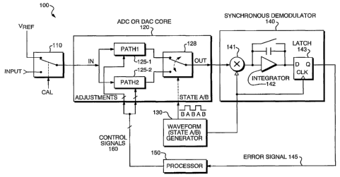
Fig. 1 is a high level illustration of a converter system 100 that operates
according to principals of the present invention. The system 10 consists of an
input
switch 110, a converter core 120, state signal generator 130, a synchronous
demodulator 140, and a processor 150. In general, the present invention is a
technique for dynamically calibrating the converter core 120, which may be a
successive approximation charge to digital converter, or some other voltage
converter, by toggling at least some portion of the converter between two
predetermined, nominally balanced, states (state A and state B).
The input switch 110 provides a converter input signal (IN) to a converter
core 120. The converter input, IN, may be selected from either a system input
voltage (INPUT), such as when the system 10 is running in its normal operating
mode, or as a reference voltage (VREF), such as when the system 10 is running
in a
calibration mode. The particular operating or calibration mode is selected by
a
switch control input signal, CAL.
In one preferred embodiment, the converter core 120 may have two physical
signal paths 125-1 and 125-2 that represent the two states, state A and state
B. In
other preferred embodiments, the converter core 120 may have a single signal
path
that operates in two different modes to provide the two different states.
When in a calibration mode, the system 10 acts as a feedback loop that has a
goal of balancing the output between the two predetermined states. When the
converter core 120 is out of balance, the voltages and/or charges in the two
states
differ, producing an error signal 145.
The two states are chosen such that they are normally expected to generate
the same output charge, OUT, at the output of the converter core 120. However,
if
the converter is not perfectly balanced, switching between the two states
generates a
square wave signal OUT that actually toggles between two values, as either of
the
two paths are alternately selected by output switch 128.
The synchronous demodulator 140 has a bandwidth centered at the state A/B
toggle frequency. Thus, the synchronous demodulator 140 can be used to
accurately detect the amount of error, even in the presence of significant
Direct
Current (DC) voltage and low frequency (1/f) noise.
CA 02571228 2006-12-15
WO 2006/009896 PCT/US2005/021568
-6-
In preferred embodiments, the synchronous demodulator 140 can be a mixer
and an integrator. The mixer 141 is typically a multipler or cross-coupled
switches.
The integrator 142 controls the bandwidth of the demodulator 140. It can be
designed to be very narrow band, to reject both low and high frequency
signals, as
well as to reject noise and DC offsets.
The integrated value of the error signal can in turn be further latched 143,
prior to the error signal 145 being fed to the processor 150. The processor
150 then
uses the error signal to apply control signals 160 that adjust the operation
of the two
signal paths in the converter core.
Fig. 2 is a more detailed diagram of one embodiment of the invention as
applied to a so-called Charge Domain Converter (QDC) system 200 operating as
an
Analog to Digital Converter (ADC). This particular QDC 200 is a successive
approximation type converter that uses a number of charge storage stages
arranged
as a serial pipeline register, so that an input source charge passes from
stage to stage
down the pipeline. A reference charge generator and a charge splitter at each
stage
generate reference signals which are optionally added to the charge as it
travels
down the pipeline. In the illustrated embodiment, there are actually two
pipelines
230-1, 230-2 that produce a serial stream of both positive and negative signal
charges corresponding to a differential signal at the pipeline outputs. The
complimentary outputs are then fed to a differential amplifier 235. This
converter
core is implemented along the lines of the QDC described in the aforementioned
U.S. Patent 5,579,007 issued to Paul.
More particularly, an input voltage to be converted is presented as a
complimentary pair of voltages, Vinp and Vinm, representing a positive (plus)
and
negative (minus) version of the input signal to be converted. Switches 220-1,
220-
2, one for each of the plus and minus paths through the converter core,
provide a
selected input signal to a respective sampler, 222-1, 222-2. The samplers 222
each
convert a respective input voltage to a charge. In normal operation mode of
the
QDC 200, these input signals are selected by the switches 220. In the
calibration
mode, however, the same cominon mode voltage, Vcm, is fed through the samplers
222 to each of the converter pipelines 230. In the preferred embodiment, Vcm,
is
equal to one-half the full scale input value. This is an input condition that
results in
the same nominal output value being provided by each of the plus and minus
paths.
CA 02571228 2006-12-15
WO 2006/009896 PCT/US2005/021568
-7-
The charges output by the samplers 222-1, 222-2 are fed to the input stage of
the respective charge pipeline 230-1, 230-2, which are implemented as Charge
Coupled Device (CCD) type analog shift registers. Each of the plus and minus
paths through the converter core 210 have a respective digital=to-analog (DAC)
ladder DACp (230-1) or DACm-(230-2).
Each ladder consists of reference charge generator 225-1, 225-2 and a series
of adjustable charge splitters 226 (not individually numbered for the sake of
clarity).
There is an adjustable charge splitter 226 associated with each stage of each
of the pipelines 230. The charge splitters 226 are arranged in series to
couple (or, to
not couple, depending upon the setting of a corresponding switch. 227) a
fractional
amount of charge to the respective stage of the pipeline 230. Each successive
splitter 226 provides one-half of the reference charge it receives to the next
splitter
in the chain. Thus, the string of splitters provide an amount of charge equal
to 1/2,
1/4, 1/8, 1/16,..., 1/2' (where i is the number of stages in the pipeline) of
the
reference charge.
In normal operation of the converter core, a set of fast comparators 229, one
for each stage of the pipeline (not shown in detail), provide an analog charge-
to-
digital conversion result.
However, of more interest to the present invention is operation in the
calibration mode. In that mode, the switches 227 are controlled instead by a
set of
switch control signals 232 provided by a digital shift register 230. In the
calibration
mode, the switches 227 are configured so that the converter core may be
operated in
one of two states, state A or state B, that nominally each provide the same
output
charge. The system is operated in the calibration mode such that it changes
between
state A and state B at a calibration or "A/B" toggle rate. The A/B toggle rate
can be
any convenient frequency at which the components of the system operate
properly.
Please note also that in the calibration mode an extra bit of the pipeline,
beyond the Least Significant Bit (LSB) used in normal operation, is enabled
for use.
The extra stage beyond the nominal LSB, as will be understood shortly,
provides the
capability for producing two nominally equal output states, within the range
of the
LSB resolution of the converter, but by actually using two different input
states.
Fig. 3 illustrates the state of the switches 227 more particularly. As alluded
to previously, the switches 227 are used to control the converter core so that
it is
CA 02571228 2006-12-15
WO 2006/009896 PCT/US2005/021568
-8-
toggled between two different states, state A and state B, that are expected
to
provide the same output value. In Fig. 3 a convention is adopted such that a
binary 1
represents a switch control signal that places its corresponding switch 227 in
the
closed state, with a binary 0 representing a switch control signal that opens
its
corresponding switch.
In a first state A, illustrated in the top two lines of Fig. 3, the plus
ladder or
DACp is fed control signals 10 0 ... 0 [0], with logic 1 being fed to control
the
switch for the first splitter 226 in the pipeline 230-1 (the one receiving 1/2
the
reference charge), so that only that stage is permitted to feed charge to the
pipeline
230-1. Please note a convention here of the bracketed value [0] indicating the
logic
state associated with the added bit which is the stage i+lth bit, beyond the
LSB stage
i. Also in state A, the minus ladder or DACm is fed control signals 0 1 1 ...
1 [1], to
allow all stages in pipeline 230-2 except the first to receive charge. Thus,
in this
state A, the differential amplifier 235 provides an output corresponding to
the
difference between these two input settings 10 0 ... 0 [0] and 0 1 1 ... 1
[1].
The additional bracketed bits provide two states that are capable of
producing the "same" output, to an accuracy of a fraction of the converter's
LSB
resolution.
State B, illustrated in the bottom two lines of Fig. 3, represents a different
state of the converter core that nominally provides the same output. In state
B, the
plus ladder DACp is fed control signals 0 1 1 ... 1 [1], and the minus ladder
DACm
is fed control signals 10 0 ... 0 [0]. Thus, in this state B, the differential
amplifier
235 provides an output corresponding to the difference between these two input
settings 0 1 1 .. 1 [1] and 10 0 ... 0 [0].
In the circuit of Fig. 3, these switch control signals are shown being
generated by feeding a square wave at the A/B toggle clock frequency. These
signals might be generated by a clock divider associated with each control
line
running at the A/B rate. However, a particular preferred embodiment of a
switch
control signal generator that uses a ring, counter is useful when A/B is
related to the
clock frequency. This implementation for the switch control signal generator
will be
described below in connection with Fig. 7.
While the outputs in states A and B should nominally be the same, and thus
the output of the differential amplifier 235 should be a constant value, in
fact the
CA 02571228 2006-12-15
WO 2006/009896 PCT/US2005/021568
-9-
output is a square wave, as illustrated, due to differences in the calibration
of DACp
and DACm.
As previously mentioned, mixer 240 and integrator 241 operate as a
synchronous demodulator (driven by the A/B state signal fed to mixer 240) to
detect
the error signal and to drive the integrator 241 output to one voltage rail or
the other.
Fig. 4A illustrates a typical output of the integrator 241 for the plus ladder
DACp, for two different operating conditions. A first condition, illustrated
by the
solid line square wave signal 401, alternates between two values at the A/B
toggle
rate. The difference in output between state A and state B under these
conditions is
Ol. The dotted line square wave 402 illustrates the output under a different
set of
operating conditions, where the difference in output is A2.
Fig. 4B illustrates the output of the integrator 241 for the two conditions.
In
the first instance, illustrated by the solid line ramp signal 403, the
integrator output
ramps to a voltage rail at time tl with slope sl. However, in the case of
dotted line
404, the integrator-output ramps more slowly with slope s2, to time t2. The
synchronous demodulator 240 thus converges rapidly wlien the differential A/B
output is large. However, it also permits resolution of smaller differences in
A/B
state output, by simply allowing a longer integration time.
Fig. 5 illustrates a phenomenon of the integrator and comparator in more
detail, and the preference for including latch 242. In particular, consider a
simple
situation where there is no offset in the calibration circuitry, and the
pipelines 230
provide a perfectly constant output in the calibration mode. In this scenario,
both
complimentary outputs of the integrator, V+ and V-, will appear as an
accumulation
of this constant voltage, that is, as continuous ramp up and ramp down signals
051
and 502, as indicated by the dotted lines with slope s 1.
However, consider when the components of the system introduce an offset.
There are several possible sources for the offset, either in the synchronous
demodulator itself, or more likely, differences introduced by the two paths
125-1,
125-2 through the converter core. As indicated by the solid line signals 503
and
504, the simple ramps now have a further sawtooth-like modulation impressed
upon
them, with the period of the sawtooth corresponding to the A/B toggle rate.
Eventually, at time t4, the ramp will remain above the impressed sawtooth. The
ramp will actually oscillate above and below sawtooth for a while after time
t3,
CA 02571228 2006-12-15
WO 2006/009896 PCT/US2005/021568
-10-
producing an unambiguous error signal. By adding the latch 243 timed to sample
the sawtooth on the edge of the A/B clock periods, this effect can be
minimized.
This is evident from the timing diagrams for the comparator output (COMP OUT),
and latch output (LATCH OUT), shows the latch-stabilized error signal 145.
Processor 150 then receives the output of latch 243 and determines the
values of adjustment signals applied to the adjustable splitters 230. If the
latch
output is equal to a logic 1, then the processor 150 will set the values of
these signals
to cause one or more of the splitters 230 to adjust a certain amount in one
direction.
If the latch output is equal to a logic value 0, then the signals are set to
values that
adjust one or more splitters 230 in the other direction. The processor 150 may
use
any convenient algorithm to converge to a splitter adjustment solution,
including,
but not limited to a binary search or a linear search.
Certain converter configurations advantageously malce use of chopper
stabilization for normal mode operation of the differential amplifier 235.
With this
type of amplifier, DC offsets and low frequency Uf noise are essentially
removed,
because the signal is shifted above DC. In these configurations, some of the
circuitry used in a typical chopper-stabilized amplifier can be used to
implement
portions of the synchronous demodulator.
Fig. 6 is a schematic diagram illustrating one such possible embodiment. As
before, the outputs of the DACm and DACp channels are provided by the buffer
amplifiers 232-1 and 232-2, respectively. The chopper stabilized amplifier 600
consists of mixer 633, differential amplifier 635 and output mixer 640. To
stabilize
the converter output in normal operation mode, the first mixer 633 up-converts
any
DC signal received from the input buffer amplifiers 232-1 and 232-2, up to
some
predetermined carrier. Differential amplifier 635 in turn operates to take a
difference at a frequency higher than DC, avoiding the introduction of further
DC
noise or low frequency 1/f noise. The output mixer 240 then down-converts the
differential amplifier output baclc to DC.
It is therefore quite evident that a synchronous demodulator needed for the
calibration mode shares many components of the chopper stabilized amplifier
600
used in the normal operation mode. In other words, amplifier 635 can serve to
function as the high speed differential amplifier 235 need for the calibration
mode of
Fig. 2, and mixer 640 can serve as the mixer 240. The first mixer 633 and
second
CA 02571228 2006-12-15
WO 2006/009896 PCT/US2005/021568
-11-
mixer 640 are each fed the A/B toggle signal. The additional mixer 633 on the
input
can be set to merely pass through the signals output by the buffers 232-1, 232-
2. In
the case of a multiplier implementation, it can be set to multiply by a value
of 1.
Finally, Fig. 7 shows a more detailed view of a possible refinement for the
switch control signal generator. If the pipeline has 36 stages, for example,
36 flip
flops would be required to provide the control signals if a simple shift
register is
used. Careful study of the sequence of bits produced by the digital shift
register
230 reveal that they are actually square waves of differing phases. For a
converter
with many pipeline stages, the control signals can be more efficiently
generated by a
ring divider instead of many flip-flops, and prudent selection of the A/B
toggle rate.
For example, if the A/B toggle rate is 1/16th of the pipeline clock rate, then
all phases of the required 8-bit on then 8-bit off waveforms can be generated
with a
single ring counter having only 8 flip flops, assuming that each flip flop
provides
true and complimentary outputs. The necessary control signals can then be
selected
from the proper phase output of the ring counter, regardless of how many
pipeline
stages there are.
While this invention has been particularly shown and described with
references to preferred embodiments thereof, it will be understood by those
skilled
in the art that various changes in form and details may be made therein
without
departing from the scope of the invention encompassed by the appended claims.