Note: Descriptions are shown in the official language in which they were submitted.
CA 02571338 2007-O1-12
MOBILE WIRELESS COMMUNICATIONS DEVICE INCLUDING AN
ELECTRICALLY CONDUCTIVE DIRECTOR ELEMENT AND RELATED
METHODS
Field of the Invention
The present invention relates to the field of communications devices, and,
more
particularly, to mobile wireless communications devices and related methods.
Background of the Invention
Cellular communications systems continue to grow in popularity and have become
an integral part of both personal and business communications. Cellular
telephones allow
users to place and receive voice calls most anywhere they travel. Moreover, as
cellular
telephone technology has increased, so too has the functionality of cellular
devices and the
different types of devices available to users. For example, many cellular
devices now
incorporate personal digital assistant (PDA) features such as calendars,
address books, task
lists, etc. Moreover, such mufti-function devices may also allow users to
wirelessly send
and receive electronic mail (email) messages and access the Internet via a
cellular network
and/or a wireless local area network (WLAN), for example.
Even so, as the functionality of cellular communications devices continues to
increase, so too does the demand for smaller devices which are easier and more
convenient
for users to carry. One challenge this poses for cellular device manufacturers
is designing
antennas that provide desired operating characteristics within the relatively
limited amount
of space available for the antenna.
One exemplary cellular antenna structure is disclosed in U.S. Patent No.
6,897,817
to Jo et al. The antenna includes a conductive top plate formed in the shape
of a spiral. In
one embodiment a sidewall meanderline extends from an edge of the top plate in
the
direction of a ground plane. A shorting meanderline connects the top plate and
the ground
plane. A first region of the top plate overlies the ground plane. A second
region of the top
plate extends beyond the ground plane. Tuning is provided by adjusting the
length and
other dimensions of the meanderlines.
For internal antennas such as the one described above which are carried within
the
housing of a cellular device, it is typically difficult for such devices to
comply with
applicable specific absorption rate (SAR) and hearing aid compatibility (HAC)
1
CA 02571338 2007-O1-12
requirements due in part to the relatively close proximity of the antenna to
the user's ear.
As such, further improvements may be desirable to help achieve desired SAR
and/or HAC
requirements.
Brief Description of the Drawings
FIG. 1 is a perspective view of a mobile wireless communications device in
accordance with the invention next to a user wearing an electronic hearing
aid.
FIG. 2 is a schematic front view of the PCB and director element of the mobile
wireless communications device of FIG. 1.
FIG. 3 is a schematic rear view of the PCB and director element of the mobile
wireless communications device of FIG. 1.
FIG. 4 is schematic side view of the PCB, director element, and housing of the
mobile wireless communications device of FIG. 1.
FIG. 5 is a schematic side view of an alternative embodiment of the PCB,
director
element, and housing of the mobile wireless communications device of FIG. 1.
FIG. 6 is a schematic front view of an alternative embodiment of the PCB and
director elements of the mobile wireless communications device of FIG. 1.
FIGS. 7 through 9 are two-dimensional beam pattern diagrams for a mobile
wireless communications device antenna at three respective operating
frequencies without
an associated director element and with an associated director element in
accordance with
the invention.
FIG. 10 is a schematic block diagram of the mobile wireless communications
device of FIG. 1 illustrating additional exemplary components thereof.
Detailed Description of the Preferred Embodiments
The present description is made with reference to the accompanying drawings,
in
which preferred embodiments are shown. However, many different embodiments may
be
used, and thus the description should not be construed as limited to the
embodiments set
forth herein. Rather, these embodiments are provided so that this disclosure
will be
thorough and complete. Like numbers refer to like elements throughout, and
prime and
multiple prime notation are used to indicate similar elements in alternative
embodiments.
Generally speaking, a mobile wireless communications device is disclosed
herein
which may include a portable housing, a printed circuit board (PCB) carried by
the
2
CA 02571338 2007-O1-12
portable housing, a wireless transceiver carried by the PCB, and an antenna
connected to
the transceiver and carried by the PCB. The mobile wireless communications
device may
further include at least one director element for directing a beam pattern of
the antenna.
More particularly, the at least one director element may include an
electrically conductive
main branch carried by the portable housing, and an electrically conductive
connector
portion extending between the main branch and the PCB. The director elements)
may
advantageously be used to direct the beam pattern of the antenna to reduce
interference
with a hearing aid of a user, for example, to advantageously improve hearing
aid
compatibility of the mobile wireless communications device, for example.
The PCB may include a top portion and a bottom portion, and the antenna may be
carried by the bottom portion of the PCB. Moreover, the PCB may have a
generally
rectangular shape with opposing sides and opposing ends, and the electrically
conductive
main branch may extend parallel with a side of the PCB. The at least one
director element
may also be a pair thereof, with a respective electrically conductive main
branch of each
director element extending parallel to a respective side of the PCB.
Furthermore, the
electrically conductive main branch may extend parallel with the rear surface
of the PCB.
The electrically conductive main branch may be carried within the portable
housing or externally of the portable housing. In addition, the PCB may
include an
antenna feed area connected to the antenna, and the electrically conductive
connector
portion may contact the PCB adjacent the antenna feed area. Also, the antenna
may have
an operating wavelength, and the electrically conductive main branch may have
a length
of about '/4 to '/2 of the operating wavelength, for example. The electrically
conductive
main branch may be an electrically conductive bar, for example. Moreover, the
electrically
conductive connector portion may extend transversely from a medial portion of
the
electrically conductive main branch. Additionally, the wireless transceiver
may be a
cellular transceiver, for example.
A method aspect is for improving hearing aid compatibility (HAC) of a mobile
wireless communications device, such as the one discussed briefly above, for a
user with
an electronic hearing aid. The method may include positioning at least one
director
element for directing a beam pattern of the antenna to reduce interference
with the hearing
aid. The at least one director element may include an electrically conductive
main branch
carried by the portable housing, and an electrically conductive connector
portion
extending between the main branch and the PCB.
3
CA 02571338 2007-O1-12
Referring initially to FIGS. 1 through 4, a mobile wireless communications
device,
such as a cellular telephone 20, is for a user 21 wearing an electronic
hearing aid 22 in an
ear 23 of the user. The cellular telephone 20 illustratively includes a
portable housing 24
and an audio output transducer 28 (e.g., a speaker) carried by the housing and
accessible to
the electronic hearing aid 22 of the user 21 adjacent the top of the housing
as shown. An
audio input transducer (i.e., microphone) is also carried by the housing 24
and accessible
to a mouth 31 of the user 21 adjacent the bottom of the housing. Although
described
herein with reference to a cellular device, it should be noted that the
present disclosure
may be applicable to other wireless communications devices such as wireless
LAN
devices, etc.
Furthermore, an antenna 35 is illustratively positioned adjacent the bottom of
the
housing 24 so that the electronic hearing aid 22 of the user 21 is
advantageously separated
from the antenna when the cellular telephone 20 is held adjacent the user's
ear 23.
Because of the increased separation thus achieved between the antenna 35 and
the
electronic hearing aid 22, the cellular telephone 20 advantageously reduces
undesired
coupling from the antenna to the electronic hearing aid without the need for
special
shielding arrangements. As a result, this configuration is beneficial from a
hearing aid
compatibility (HAC) standpoint. Moreover, this also helps reduce SAR, as will
be
appreciated by those skilled in the art.
The cellular telephone 20 further illustratively includes a printed circuit
board
(PCB) 37 carried by the housing 24, and the antenna 35 and a wireless (e.g.,
cellular)
transceiver 38 are carried by the PCB. Of course, these components may be
carried on the
back surface or in positions other than those shown in other embodiments.
The PCB 37 illustratively includes an antenna feed area 40 where the antenna
35
connects to the wireless transceiver 38. The antenna 35 may include a
plurality of
conductive traces on the PCB 37, for example, as will be appreciated by those
skilled in
the art. As noted above, the positioning of the antenna 35 adjacent a bottom
of the housing
24 advantageously reduces coupling to the electronic hearing aid 22 of the
user 21,
however the antenna may be located elsewhere in different embodiments. The
cellular
telephone 20 may further include other components connected to the PCB 37 such
as a
display, battery, keypad, processing circuitry, etc., as will be discussed
further below.
The cellular telephone 20 further illustratively includes one or more director
elements 30 for directing a beam pattern of the antenna 35. More particularly,
the director
4
CA 02571338 2007-O1-12
element 30 illustratively includes an electrically conductive main branch 32
carried by the
housing 24, and an electrically conductive connector portion 33 extending
between the
main branch and the PCB 37. The director element 30 is advantageously used to
direct the
beam pattern of the antenna 35 to further reduce interference with the
electronic hearing
aid 22 of the user 21, for example, to advantageously improve hearing aid
compatibility of
the cellular telephone 20. That is, by directing the beam pattern of the
antenna 35 such that
the main lobe gain is directed away from the ear 23, and thus the electronic
hearing aid 22,
of the user 21, this advantageously reduces the interference with the
electronic hearing aid,
as will be appreciated by those skilled in the art.
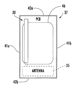
As seen in FIGS. 2 and 3, the PCB 37 illustratively has a generally
rectangular
shape with opposing sides 41a, 41b and opposing ends 42a, 42b, and the
electrically
conductive main branch 32 extends parallel with a rear surface of the PCB. The
electrically conductive connector portion 33 extends transversely from a
medial portion 45
of the electrically conductive main branch 32 and connects the main branch to
a ground
plane 46 on the back surface of the PCB 37. While the electrically conductive
connector
portion 33 is shown as a relatively short and straight connector bar in the
illustrated
example, the connector portion may take various shapes, such as a sawtooth
shape, etc.
Moreover, the electrically conductive connector portion 33 may be a mechanical
connector such as a spring connector, etc.
The electrically conductive main branch 32 is an electrically conductive bar
in the
illustrated example, although other shapes may be used in different
embodiments. By way
of example, the electrically conductive main branch 32 may include curved or
sawtooth
meanders, loops, or other features used to affect the electrical length of the
main branch,
as will be appreciated by those skilled in the art. The electrically
conductive main branch
32 may have a width of about 5 to 7 mm, for example, although other widths may
also be
used depending upon the given implementation.
The length of the electrically conductive main branch 32 is preferably about
'/4 to
'/2 of the operating wavelength of the antenna 35, for example, to provide
desired beam
steering for SAR reduction and HAC improvement, but here again other lengths
may also
be used. Moreover, positioning the electrically conductive connector portion
33 to contact
the PCB 37 adjacent the antenna feed area 40 may also assist in this regard by
providing
greater influence over the direction of beam pattern of the antenna 35.
CA 02571338 2007-O1-12
By way of comparison, FIGS. 7 through 9 each illustrate a measured two-
dimensional beam pattern 70, 80, 90 for the antenna 35 without an associated
director
element 30, as well as beam patterns 71, 81, 91 for the antenna with two
associated
director elements 30, respectively. More particularly, the two director
elements 30 were
positioned on the back side of the PCB 37 (i.e., similar to the embodiment
illustrated in
FIGS. 1-4 but with two spaced apart director elements instead of a single
director
element). The beam patterns 70, 71 correspond to an operating frequency of
1850 MHz,
the beam patterns 80, 81 correspond to an operating frequency of 1880 MHz, and
the
beam patterns 90, 91 correspond to an operating frequency of 1910 MHz.
In the present example, the electrically conductive main branch 32 is carried
within
the housing 24 on an inside sidewall thereof, as seen in FIG. 4. As such, in
this
embodiment rather than a bar the electrically conductive main branch 32 could
be
implemented by metallizing the sidewall of the housing 24, for example.
Moreover, an air
gap 47 is shown between the PCB 37 and the electrically conductive main branch
32, but
in some embodiments this space may be filled with a solid dielectric, for
example. The
electrically conductive main branch 32 may also be partially or completely
enclosed
within the sidewall of the housing 24.
Turning now additionally to FIG. 5, in an alternative embodiment the
electrically
conductive main branch 32' may be carried externally of the portable housing
24', i.e., on
an outside surface thereof, as shown. In another alternative embodiment, a
pair of director
elements 30a', 30b' are included with respective electrically conductive main
branches
32a', 32b' extending parallel to a respective side 41a', 41b' of the PCB 37
(FIG. 6).
A method aspect is for improving hearing aid compatibility (HAC) of a mobile
wireless communications device 20 for a user with an electronic hearing aid
22. The
method may include positioning at least one director element 30 for directing
a beam
pattern of the antenna 35 to reduce interference with the electronic hearing
aid 22. As
noted above, the at least one director element 30 may include an electrically
conductive
main branch 32 carried by the portable housing 24, and an electrically
conductive
connector portion 33 extending between the main branch and the PCB 37.
Other exemplary components of a hand-held mobile wireless communications
device 1000 are now described in the example below with reference to FIG. 10.
The
device 1000 illustratively includes a housing 1200, a keypad 1400 and an
output device
1600. The output device shown is a display 1600, which is preferably a full
graphic LCD.
6
CA 02571338 2007-O1-12
Other types of output devices may alternatively be utilized. A processing
device 1800 is
contained within the housing 1200 and is coupled between the keypad 1400 and
the
display 1600. The processing device 1800 controls the operation of the display
1600, as
well as the overall operation of the mobile device 1000, in response to
actuation of keys on
the keypad 1400 by the user.
The housing 1200 may be elongated vertically, or may take on other sizes and
shapes (including clamshell housing structures). The keypad may include a mode
selection
key, or other hardware or software for switching between text entry and
telephony entry.
In addition to the processing device 1800, other parts of the mobile device
1000 are
shown schematically in FIG. 10. These include a communications subsystem 1001;
a
short-range communications subsystem 1020; the keypad 1400 and the display
1600,
along with other input/output devices 1060, 1080, 1100 and 1120; as well as
memory
devices 1160, 1180 and various other device subsystems 1201. The mobile device
1000 is
preferably a two-way RF communications device having voice and data
communications
capabilities. In addition, the mobile device 1000 preferably has the
capability to
communicate with other computer systems via the Internet.
Operating system software executed by the processing device 1800 is preferably
stored in a persistent store, such as the flash memory 1160, but may be stored
in other
types of memory devices, such as a read only memory (ROM) or similar storage
element.
In addition, system software, specific device applications, or parts thereof,
may be
temporarily loaded into a volatile store, such as the random access memory
(RAM) 1180.
Communications signals received by the mobile device may also be stored in the
RAM
1180.
The processing device 1800, in addition to its operating system functions,
enables
execution of software applications 1300A-1300N on the device 1000. A
predetermined set
of applications that control basic device operations, such as data and voice
communications 1300A and 1300B, may be installed on the device 1000 during
manufacture. In addition, a personal information manager (PIM) application may
be
installed during manufacture. The PIM is preferably capable of organizing and
managing
data items, such as e-mail, calendar events, voice mails, appointments, and
task items. The
PIM application is also preferably capable of sending and receiving data items
via a
wireless network 1401. Preferably, the PIM data items are seamlessly
integrated,
7
CA 02571338 2007-O1-12
synchronized and updated via the wireless network 1401 with the device user's
corresponding data items stored or associated with a host computer system.
Communication functions, including data and voice communications, are
performed through the communications subsystem 1001, and possibly through the
short-
range communications subsystem. The communications subsystem 1001 includes a
receiver 1500, a transmitter 1520, and one or more antennas 1540 and 1560. In
addition,
the communications subsystem 1001 also includes a processing module, such as a
digital
signal processor (DSP) 1580, and local oscillators (LOs) 1601. The specific
design and
implementation of the communications subsystem 1001 is dependent upon the
communications network in which the mobile device 1000 is intended to operate.
For
example, a mobile device 1000 may include a communications subsystem 1001
designed
to operate with the MobitexTM, Data TACTM or General Packet Radio Service
(GPRS)
mobile data communications networks, and also designed to operate with any of
a variety
of voice communications networks, such as AMPS, TDMA, CDMA, PCS, GSM, etc.
Other types of data and voice networks, both separate and integrated, may also
be utilized
with the mobile device 1000.
Network access requirements vary depending upon the type of communication
system. For example, in the Mobitex and DataTAC networks, mobile devices are
registered on the network using a unique personal identification number or PIN
associated
with each device. In GPRS networks, however, network access is associated with
a
subscriber or user of a device. A GPRS device therefore requires a subscriber
identity
module, commonly referred to as a SIM card, in order to operate on a GPRS
network.
When required network registration or activation procedures have been
completed,
the mobile device 1000 may send and receive communications signals over the
communication network 1401. Signals received from the communications network
1401
by the antenna 1540 are routed to the receiver 1500, which provides for signal
amplification, frequency down conversion, filtering, channel selection, etc.,
and may also
provide analog to digital conversion. Analog-to-digital conversion of the
received signal
allows the DSP 1580 to perform more complex communications functions, such as
demodulation and decoding. In a similar manner, signals to be transmitted to
the network
1401 are processed (e.g. modulated and encoded) by the DSP 1580 and are then
provided
to the transmitter 1520 for digital to analog conversion, frequency up
conversion, filtering,
8
CA 02571338 2007-O1-12
amplification and transmission to the communication network 1401 (or networks)
via the
antenna 1560.
In addition to processing communications signals, the DSP 1580 provides for
control of the receiver 1500 and the transmitter 1520. For example, gains
applied to
communications signals in the receiver 1500 and transmitter 1520 may be
adaptively
controlled through automatic gain control algorithms implemented in the DSP
1580.
In a data communications mode, a received signal, such as a text message or
web
page download, is processed by the communications subsystem 1001 and is input
to the
processing device 1800. The received signal is then further processed by the
processing
device 1800 for an output to the display 1600, or alternatively to some other
auxiliary I/O
device 1060. A device user may also compose data items, such as e-mail
messages, using
the keypad 1400 and/or some other auxiliary I/O device 1060, such as a
touchpad, a rocker
switch, a thumb-wheel, or some other type of input device. The composed data
items may
then be transmitted over the communications network 1401 via the
communications
subsystem 1001.
In a voice communications mode, overall operation of the device is
substantially
similar to the data communications mode, except that received signals are
output to a
speaker 1100, and signals for transmission are generated by a microphone 1120.
Alternative voice or audio I/O subsystems, such as a voice message recording
subsystem,
may also be implemented on the device 1000. In addition, the display 1600 may
also be
utilized in voice communications mode, for example to display the identity of
a calling
party, the duration of a voice call, or other voice call related information.
The short-range communications subsystem enables communication between the
mobile device 1000 and other proximate systems or devices, which need not
necessarily
be similar devices. For example, the short-range communications subsystem may
include
an infrared device and associated circuits and components, or a BluetoothTM
communications module to provide for communication with similarly-enabled
systems
and devices.
Many modifications and other embodiments will come to the mind of one skilled
in the art having the benefit of the teachings presented in the foregoing
descriptions and
the associated drawings. Therefore, it is understood that various
modifications and
embodiments are intended to be included within the scope of the appended
claims.
9