Note: Descriptions are shown in the official language in which they were submitted.
CA 02571801 2006-12-21
WO 2006/002335 PCT/US2005/022364
DIE ATTACH AREA CUT-ON-FLY METHOD AND APPARATUS
SPECIFICATION
FIELD OF INVENTION
[0001] This invention is related to security tags, and, in particular, to
bonding integrated circuits
(ICs) uniquely suited to high volume tag production.
BACKGROUND OF THE INVENTION
[0002] Chip bonding is costly. The two largest components of the cost of RFID
tags today are
the integrated circuit and the attachment of that circuit to an antenna
structure. Moore's law and
increasing volume are helping to drive the IC cost down, but bonding is a
mechanical process and
does not benefit from the same technology advances or economies of scale.
[0003] Current methods of chip bonding do not adequately address cost. A two-
step approach of
an intermediary "strap" achieves incremental cost improvement by relocating
the costs. However,
straps do not address the problem directly, as bonding is still required, but
to a smaller tag.
Moreover, straps add another step to bond the strap to the big tag.
[0004] Current manufacturers using standard bonding technology with straps,
want straps to be
like traditional bonding surfaces, that is, hard and inflexible. But such
straps do not lend themselves
to easy integration into squishy flexible tags. The known standard bonding
processes are all strap-
based solutions, and therefore less than ideal.
[0005] One related art bonding method, called fluid self-assembly, provides
insufficiently robust
bonds. Because the chips find their own way into bonding sockets, the chips
cannot use any
adhesives or flux, since anything sticky prevents free motion of the chip into
the sockets. Then the
bond is made at a tangent between the chip bonding pad and the side of the
bonding cavity. This flat-
to-edge bond is different than and less reliable than traditional bonds, which
are made flat-to-flat. As
an analogous example illustrating problems inherent to flat-to-edge bonds,
consider trying to stand a
playing card on edge, rather than laying it flat on a table. Fluid self-
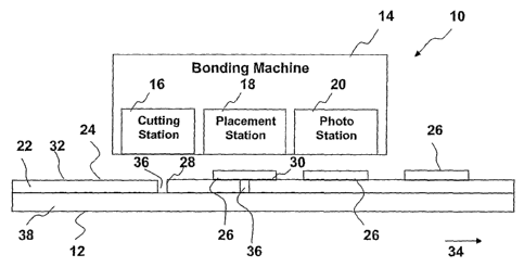
assembly also places restrictions
on the type of substrate that can be used. This may not be a problem for just
making straps; but it is
certainly a problem for foregoing the strap and putting the chip right on the
tag.
[0006] A known bonding process is a gallant brute force attempt to make
standard bonding
faster. Instead of having one vacuum head pick up one chip and place it on one
strap, a plurality of
heads (e.g., 60) in lock step picks up that number (e.g., 60) of chips and
puts them on that number
1
CA 02571801 2006-12-21
WO 2006/002335 PCT/US2005/022364
(e.g., 60) of straps. This process suffers from the problem of keeping all of
the number (e.g., 60) of
chips aligned correctly at the same time.
[0007] Bonding RFID chips is more like processing diodes and resistors than
processing other
kinds of chips. One new RFID strap line uses a traditional tape automated
bonding process, with a
sprocket-fed 35 mm tape of hard straps inching its way through a traditional
flip-chip placement and
bonding head. At 4.75 mm pitch, four lanes wide, and 10,000 chip bonds per
hour, their tape
advances through the bonding procedure at about 0.65 feet per minute. It would
be beneficial if a
chip bonding process could produce more bonded chips in less time.
[0008] In order to consider why the art has not bonded chips as exemplified by
the preferred
embodiments of the invention discussed below, it may help to compare standard
electronic chip
components to RFID tags. Standard electronic chip components are known and
generally found on
printed circuit boards. A bare IC is bonded to a carrier by wire bonding or
flip chip. Then a package
is molded around the carrier and chip. The package is then put onto a printed
circuit board via thru-
hole or surface mount assembly. In summary, typical standard chip components:
need to be
compatible with multiple PCB assembly technologies, including solder baths,
solder waves, IR
reflow, and a variety of cleaning and baking steps; want more and more
computational power put in
single chip assemblies; and are made to last. In contradistinction, RFID tags:
are never soldered or
baked or cleaned; are complete unto themselves and do not have to be
integrated into any other
system; want the bare minimum computational power to minimize cost and energy
consumption
(which translates into read distance); and do not face the same power
dissipation or environmental
requirements as standard chips.
[0009] To meet their design requirements, standard chip assemblies usually
start with relatively
stiff and heavy substrates, at least compared to RFID tags. Ceramics and
fiberglass are common.
These are meant to be tough and resistant to thermal influences. Usually the
standard chip substrates
are etched. Laser cutting is expensive because the standard chip substrates
are thick and have high
thermal masses.
[0010] RFID tags are substantially different. The metal layer is thin and
flexible (or non-rigid)
by comparison. The back or substrate of each tag is soft polypropylene or
paper. The substrates are
easily to punch, cut, dimple, and weld. The preferred embodiments of the
invention reinvent
bonding taking advantage of these different properties.
[0011] A known wire bonding process is disclosed in U.S. Patent No. 5,708,419
to Isaacson, et
al., the contents of which are incorporated by reference herein in its
entirety. Isaacson discusses the
2
CA 02571801 2006-12-21
WO 2006/002335 PCT/US2005/022364
bonding of an IC to a flexible or non-rigid substrate which generally can not
be subjected to high
temperatures, such as the temperature required for performing soldering
processes. In this wire
bonding process, a chip or dye is attached to a substrate or carrier with
conductive wires. The chip is
attached to the substrate with the chip front-side face up. Conductive wires
are bonded first to the
chip, then looped and bound to the substrate. The steps of a typical wire
bonding process include:
1. advancing web to the next bond site
2. stopping
3. taking a digital photograph of the bond site
4. computing bond location
5. picking up a chip
6. moving the chip to the bond site
7. using photo feedback to adjust placement to the actual site location
8. placing or depositing chip
9. photographing the chip to locate the bond pads
10. moving the head to the chip bond pad
11. pressing down, vibrating and welding conductive wire to the bond pad
12. pulling up and moving the chip to the substrate bond pad, trailing wire
back to the chip
bond
13. pressing down and welding that bond
14. pulling up and cutting off the wire; and
15. repeating steps 10-14 for each connection
[0012] In contrast, the interconnection between the chip and substrate in flip-
chip packaging is
made through conductive bumps of solder that are placed directly on the chip
surface. The bumped
chip is then flipped over and placed face down, with the bumps electrically
connecting to the
substrate.
[0013] Flip chip bonding, a current state of the art process, is expensive
because of the need to
match each chip to a tiny, precision-cut bonding site. As chips get smaller,
it becomes even harder to
precisely cut the bonding site. However, the flip-chip bonding process is a
considerable advancement
over wire bonding. The steps of a typical flip-chip bonding process include:
3
CA 02571801 2006-12-21
WO 2006/002335 PCT/US2005/022364
1. advancing web to the next bond site
2. stopping
3. photographing the bond site
4. computing the bond location
5. picking up the chip
6. moving the chip to the bond site
7. using photo feedback to adjust placement at the actual site location
8. placing the chip
9. ultrasonically vibrating the placement head to weld chip in place; and
10. retracting the placement head
[0014] Steps 1 through 8 of each of the above bonding processes are
substantially the same. The
web must stop to locate the conductive gap in the substrate and precisely
place the IC. The related
art processes require that the web is stopped and measured (e.g.,
photographing the bond site,
containing the bond location, using photo feedback to adjust placement at the
actual site location) so
that the chip can be accurately placed as desired adjacent the gap and bonded.
[0015] In designing an efficient chip placement process that can be integrated
into RFID tags, the
inventors discovered that it is beneficial to avoid anything that is not
consistent with a continuous
rolling printing press. Stopping and starting the line always slows things
down. It would be
beneficial to adjust tooling to operate on a chip that is continuously
advancing down the line at a
known rate of travel.
[0016] Retracing a path during the bonding process takes time, causes
vibration, and wears
mechanical linkages. These linkages also create uncertainty in absolute
position. Rotating or
continuous devices are thus preferred over reciprocating devices.
[0017] The greater the number of mechanical connections in a bonding process,
the less certainty
there is in precise position. Every jointed or flexible linkage introduces a
certain amount of
randomness as the web and chips wiggle around. IC dimensions are tiny. It does
not take a lot of
mechanical links to move chip placement out of critical alignment.
[0018] With security tags, you cannot rely on any precise dimension set
previously. The relative
position of things varies across the web, from one end of the roll to another,
from place to place, and
from time to time. That is simply the reality of working with inexpensive
materials. For IC bonding
processes, the manufacturer must constantly adapt to how the material is
really behaving, rather than
counting on it to behave as intended.
4
CA 02571801 2006-12-21
WO 2006/002335 PCT/US2005/022364
BRIEF SUMMARY OF THE INVENTION
[0019] An integrated circuit bonding process according to the preferred
embodiments provides:
= A high quality and high reliability integrated circuit attachment to a tag
or strap;
= Bonding speeds compatible with flexographic printing lines, and thereby
suitable for
integration in current and foreseeable tag production lines; and
= Low total bond costs, for example, of less than $0.01 at production volumes.
[0020] While not being limited to a particular theory, the preferred
embodiments of the present
invention illustrate approaches for cutting a bond site and assembly-placing a
chip (e.g., transponder)
at the bond site without stopping the web. That is, the chip substrates move
continuously during the
chip placement process. In a first preferred embodiment, the bond site is cut
to form a gap where a
chip is expected to be placed. According to a second preferred embodiment, the
bond site is cut to
form the gap simultaneously with or after the chip is placed. According to the
preferred
embodiments of the present invention, a manufacturer can achieve bonding rates
for tiny chips 100
times faster than the conventional technology, in particular, by applying the
bonding process on chip
substrates moving continuously at a speed normally applicable to high speed
printing presses in the
flexographic process range of up to at least about 300 feet per minute.
BRIEF DESCRIPTION OF SEVERAL VIEWS OF THE DRAWINGS
[0021] The invention will be described in conjunction with the following
drawings in which like
reference numerals designate like elements and wherein:
Fig. I shows a table of chip locations during a time sequence in accordance
with the preferred
embodiments of the invention;
Fig 2. illustrates a structural representation of a cut-on-fly apparatus in
accordance with the
preferred embodiments;
Fig. 3 illustrates a chip placement approach in accordance with the preferred
embodiments of
the invention;
Fig. 4 shows a table of chip locations during a time sequence in accordance
with the preferred
embodiments of the invention;
Fig. 5 illustrates a bonding machine in accordance with the preferred
embodiments;
Fig. 6 shows a table of chip locations during a time sequence in accordance
with the preferred
embodiments of the invention;
CA 02571801 2006-12-21
WO 2006/002335 PCT/US2005/022364
Fig. 7 illustrates a structural representation of the placement and cutting
approach in
accordance with the preferred embodiments;
Fig. 8 shows a table of chip locations during a time sequence in accordance
with the preferred
embodiments; and
Fig. 9 illustrates a structural representation of the cut-on-fly approach of
the preferred
embodiments of the invention.
DETAILED DESCRIPTION OF PREFERRED EMBODIMENTS OF THE INVENTION
[0022] According to the preferred embodiments, RFID chips are bonded on soft,
mutable
substrates. The chips are prepared for bonding according to known chip
prepping methods. As one
example, the chips are topped with quartz - silicon dioxide - with little
windows etched down to
aluminum contact pads. These contact pads are "bumped" with solder by either
sputtering the solder
on or running the wafer across a solder wave bath. The solder sticks to the
aluminum and slides
away from the quartz.
[0023] The preferred bonding process starts with a completed silicon wafer,
which contains
thousands of integrated circuits (ICs) etched into a single plate of silicon
material. The completed
silicon wafer is cut into hundreds of the individual chips, with each chip
including an IC and its
corresponding section of the silicon plate.
[0024] Wafers with big chips (e.g., .25 inz to 1.0 inz) on them are normally
cut apart with
delicate diamond saws. In comparison, RFID chips are really, really tiny
(e.g., 50 gm x 100 gm), and
.sawing the wafer apart is not economical. For RFID chips, the wafer is
grinded on the backside to
make the wafer as thin as possible while being supportive as desired. Then the
thinned wafer is
masked with acid-resist for protection, except in the places of the wafer that
we want to cut. This is
known as a standard wafer operation.
[0025] Next the whole wafer is dipped in acid. The acid eats away the
unprotected silicon
between chips until the wafer breaks apart into thousands of chips. Using a
strainer to keep the chips
from flushing away, the acid is rinsed out of the bath leaving thousands of
RFID chips floating in a
bottle of water. The chips are poured out of the solution and dried. Using
this standard technology, a
wafer is separated into numerous chips without frictional (e.g., saw) cutting.
[0026] Most chip bonding processes struggle to either get the chip lined with
the substrate or get
both the substrate and the bond site lined up. However, the preferred
embodiments do not need that
same level of precision as previously required for chip placement. While not
being limited to a
6
CA 02571801 2009-04-03
particular theory, the preferred bonding approach described in greater detail
below just needs to get
all the chips facing about the same direction.
[0027] A shaker table, as known in the art, accomplishes the goal of chip
orientation. To begin, a
jumble of chips is placed on a funnel-shaped shaking table leading to a small
square or rectangular
(e.g., tens hundreds, thousands) alignment tube. The chips are typically
substantially box-like
rectangular prisms, possibly having slanted sides from the etching process.
The chips are shaken into
the tube, ending up in one of eight orientations. Then a picture of the shaker
chips is taken. If a chip
is in the right orientation, it continues down the tube. If a chip is not in
the correct orientation, then
the disoriented chip is kicked back onto the shaker table for another
orientation attempt. Eventually
all the chips end up in the tube in the right orientation.
[0028] In stark contrast to prior art approaches that prepare the bond site
for the IC before the
substrate goes into the bonding machine, the preferred approach of this
invention lets the bonding
machine itself make the cut. What goes into the machine for the bonding site
is solid metal. For
example, the metal is preferably a thin strip of metal film on a strap, a web
of tags, packaging
material, or a product. The important thing is that, according to the
preferred embodiments, the bond
site is not prepared (e.g., formed with a conductive gap) before the metal is
input to the bonding
machine. According to the preferred embodiments, what goes into the bonding
machine is a blank
metal strip, ready to be cut for its particular chips.
[0029] It is understood that a shaker table is one of various approaches to
accomplish chip
orientation before chip placement at a bond site, and that the invention is
not limited to this particular
approach. In fact, the preferred cut-on-f ly method is applicable to a chip
attached to its substrate, or
to a chip about to be attached to its substrate, or to a chip being attached
to its substrate.
Accordingly, the manner in which the chip is attached to its substrate is not
a limiting factor to the
preferred methods for cutting the substrate, as long as the chip is attached
or oriented for attachment
to the substrate, as discussed, by example, in greater detail below. Another
approach that
accomplishes chip orientation, for example by formation of the chip on a metal
substrate is disclosed
in U.S. publication Numbers: US2005/ 0183817A I entitled "Tag and System for
Fabricating a Tag Capable
of including an Integrated Surface Processing System"; US2005/0184873Al
entitled "A Tag Having
Patterned Circuit Elements and a Process for Making Same"; and US200510
184872A 1 entitled "A Method for
Applying an Identification Marking to an Item to Identify the Item in Response
to an Interrogation
Signal", and published on August 25, 2005.
7
CA 02571801 2006-12-21
WO 2006/002335 PCT/US2005/022364
[0030] Now it is not enough that the machine makes a cut. The cut must form a
conductive gap
in the metal strip. That is, the conductive strip or substrate material must
be removed completely at
the gap to avoid the risk that it will short out the chip later. There are at
least two-ways to down this.
One is called a "kiss cut" achieved with cutting blades. Another is ablation
with a laser - literally
vaporizing the unwanted metal. Lasers are preferred because laser cutters can
make a precise cut
without bringing anything mechanical in touch with the substrate. But, whether
by kiss cut, laser or
an equivalent approach (e.g., wafer), the bonding machine of the preferred
embodiments can make
this cut without ever slowing the web down. That is, the web is continuously
moving when the gap
is formed by the cut, and during chip placement, for example, at flexographic
printing speed.
Moreover, the cut is made within the tolerance allowed by small RFID chips
having a size of, for
example, about 100 microns or less. The tolerance allowed to create a gap
between contact points of
the chip is less than about 80 microns, and more preferably, less than about
20-30 microns.
[0031] The preferred examples of the embodiments discuss the invention with
relation to chips
(e.g., transponders) having two conductive pads requiring electrical
connections to an antenna at a
die attach site with a gap formed from a single cut. It is understood,
however, that the invention is
not limited to that scope, as the preferred embodiments apply to other types
of chips (e.g., multi-
padded chips) as well. Of course, multi-padded chips need more cuts, which is
easily provided,
especially using laser cutters, which can cut the conductive substrate or
carrier in a preconfigured
pattern as desired.
[0032] The width of the cut, in particular a laser cut, is largely a function
of the pattern and the
magnitude of energy applied. The width is also a function of the thickness of
the conductive
substrate, as the thicker the substrate, the more difficult it is to get a
clean narrow cut. Using pulse
control laser cutting, femto second resolution is possible. For
micromachining, water saws are
another preferred approach for cleaning the kerf. Regardless of the cutting
approach, the preferred
cut width is about 5 gm or less.
[0033] To avoid wimpy unstable bonds, the bonding machine of the preferred
embodiments
welds the chips to the substrate. The preferred bond is with a solder weld,
and for that it is nice to
use flux, perhaps even acid flux. There is no need for exact precision. Flux
is simple squirted over
the bond area for each solder weld. The flux forms a pre-defined boundary that
solder bumps (e.g.,
flip, chip, controlled chip collapse) of the chip don't go beyond. The solder
bumps adhere to the flux
and orient to the metal along the web direction.
8
CA 02571801 2006-12-21
WO 2006/002335 PCT/US2005/022364
[0034] There are various approaches to transfer the chips (e.g., transponders)
from the alignment
tube of, for example, a shaker table, to the sticky flux over the bond area as
the web goes by. One
approach for depositing or placing chips is to tip the chips on, letting the
chips contact the moving
flux such that a leading end of the chips stick to and get pulled out by the
flux, one at a time.
Another approach is to shoot the chips onto the flux with air pressure. A
preferred approach is to
stick the aligned chips with a rotating wheel of vacuum heads. For example, as
shown in Fig 3, each
head sucks a chip out of the alignment tube at the top of the wheel's turn,
and blows it onto the bond
site on the bottom of its turn. It is preferable to place or deposit the chip
upside down in the flux, so
that the chip's solder bumps are pressed right into the conductive material
(e.g., metal strip) for
connection at the bonding site.
[0035] While not being limited to a particular theory, the chip placement can
be achieved without
slowing the web down to place the chips. The web keeps whizzing by, and the
bonding machine
places a chip onto the moving web as desired, for example, every time an
available chip flux spot
shows up. This approach for chip bonding on soft substrate thus is more like
mechanical assembly
processing than like anything used in standard IC processing.
[0036] Next, in the preferred embodiments, a picture is taken to determine
where the chip landed.
From that picture the bonding machine can compute where it should or should
have cut the metal
strip to make the bonding site for that chip. That is, this photo information
can be used to determine
where to make the cut after the chip is placed. As discussed in greater detail
below, the photo
information can also be used to cut the conductive material (e.g., metal
strip) at the bond site before
the chip is attached to the conductive material.
[0037] The preferred approach described herein creates a conductive gap in the
antenna right
where the chip is sitting or expected to sit. The most preferred embodiments
take the information of
where this bond site should be, and uses this information to cut the bond site
for a chip that has not
been placed onto its bond site. In other words, the optical or alignment
feedback of a placed chip is
used to determine and cut the bond site for a subsequent pre-bonded chip
(e.g., the next chip) yet to
be placed.
[0038] The preferred embodiments use photo feedback because while the chips do
not change in
dimension, the substrates do change - especially soft substrates. On a roll of
tags, which may be
made in one location (e.g., Puerto Rico) and bonded in another location (e.g.,
Sweden), the difference
in the location of a pre-cut bond site from one end of the roll to the other
end is much larger than
reasonably allowable for the chips. Webs and rolls stretch; machines wobble;
components heat up
9
CA 02571801 2006-12-21
WO 2006/002335 PCT/US2005/022364
and expand. Thus when a tag is brought into a bonding machine, the
bonding,machine does not
know and cannot predict exactly where the bond site will be. However, if the
bonding machine
knows where the last bond site should have been, there is no substantial error
in placing the current
or next bond site there. In other words, there is no substantial error in
placing a next or subsequent
chip based on the location of a previous chip.
[0039] In fact, the difference between one, two, three, or maybe even ten bond
sites in a row is
small (e.g., almost zero, nearly identical in placement) and insignificant as
within the allowable
margin of error between the contact pads of the chips (e.g., about 10 to 30
gm). So it is not necessary
for the bonding machine to place a chip based on the photographed location of
the previous chip.
The bonding machine has more time to process the photo and can use the photo
of a deposited chip
to place a subsequent chip several chips removed from the photographed chip.
The cutting device
just makes the cut that much longer before the photo step. However, the little
errors add up, for
example, 50 tags later the cutting device may not make the right cut between
the expected location of
the contact pads with certainty. With a million tags on a roll, there is no
way that one cut position is
right for all of the chips.
[0040] Accordingly, the most preferred embodiments of the invention use
alignment feedback.
The inventors have discovered that a preferred way to use alignment feedback
is to locate a deposited
chip to make the cut for a subsequent chip before that subsequent chip is
placed. It is understood that
the invention is not limited to a placement machine that uses photo feed back.
In fact, as will be
described in greater detail below, alignments can be accomplished by
approaches other than photo.
For example, the placement of a chip and cutting of the die attach area could
be aligned based on the
placement of the flux.
[0041] After the chips are deposited on to their respective bond site, they
are welded to the metal
substrate. Solder welds are preferred because they do not corrode, they
provide mechanical strength,
and they form a metallurgical bond for superior conduction. That is, a closer
weld provides a high
quality and highly reliable conductive attachment. The preferred soldering
technique is a type of
flip-chip soldering known as controlled chip collapse.
[0042] In the preferred embodiments, the solder is present as bumps on the
chip placed onto the
flux. Heat is applied to the solder, but not too much heat. The preferred
amount of heat is sufficient
to get the surface of the flux and substrate adjacent the flux hot, and
liquefy the solder, but not to
burn or deform the substrate. The substrate is soft, possibly with a plastic
layer if the bonding
machine is bonding to an etched tag, so excessive heat should be avoided.
Flash fusing (e.g., with a
CA 02571801 2006-12-21
WO 2006/002335 PCT/US2005/022364
xenon bulb) is preferred for the solder weld. Xenon tube flash fusing is
currently used, for example,
in laser printers.
[0043] It is understood that there are numerous possible bonding methods and
the invention is
not limited to a particular approach. For example, an alternative bonding
approach to controlled chip
collapse is with the use of anisotropic conductive adhesives.
[0044] A preferred embodiment for bond site formation is exemplified in Figs.
1-3. Fig 1 shows
a table of chip locations during a time sequence, and Fig. 2 shows a
structural representative of a cut-
on-fly apparatus 10. As can best be seen in Fig. 2, a substrate 12 moves under
a bonding machine 14
from a cutting station 16 to a placement station 18 and then to a photo
station 20. In this example,
the cutting station 16 cuts a conductive layer 22 of metal and flux 24 at an
estimated die attach area
28. The placement station 18 places a chip 26 onto the substrate 12 at a bond
site 30, which includes
the conductive layer 22, preferably at each time period, as will be discussed
in greater detail below.
The photo station 20 measures the location of a chip 26 to determine the
location of a subsequent die
attach area 32 that is to be cut. While not being limited to a particular
theory, the photo station 20 is
preferably a flash vision system that looks for an edge (e.g., front edge,
rear edge) of each chip 26
passing by to determine the location of each chip.
[0045] Referring to Figs. 1 and 2, at Time 1, Chip 1 is placed at the bond
site 30 on the
conductive layer 22 of the substrate 12 as the substrate continuously moves
down the line along a
processing direction 34. At Time 2, which is subsequent to Time 1, Chip 1 is
moved to the photo
station 20 where a measurement of the chip's location is made, and Chip 2 is
placed at the bond site
30 on the conductive layer 22 of the substrate 12 at the next die attach area.
Based on the
measurement of Chip 1, the system (e.g., bonding machine 14) preferably
determines where
subsequently placed chips 26 should be placed on the substrate 12. As one of
ordinary skill in the art
would readily understand, the position of the subsequently placed chip 26 can
be determined from
knowledge of the location of Chip 1 on the substrate 12 and the distance
between successive chip
placement locations. The distance between successive chip placement locations
is understood as a
function of the delta in time between chip placements and the speed of the non-
stopping and non-
reciprocating substrate 12 moving along the processing direction 34. The
placement of each cut
through the conductive layer 22 is between the estimated locations of where
the conductive contact
points of each deposited chip 26 will be located, that is, at the estimated
die attach area 28, and is
preferably midway between the contact points, which may be separated by
microns (e.g., less than 10
m to about 100 m and most preferably between about 10 gm and 20 m).
Therefore, the
11
CA 02571801 2006-12-21
WO 2006/002335 PCT/US2005/022364
dimensions of the chip 26 and its contact points should also be known in
determining the cutting
locations for subsequently placed chips.
[00461 Accordingly, based on the measurement of Chip 1's location, the bonding
machine 14
determines where a subsequent chip should be placed and at Time 3 cuts the
conductive layer 22 at
the estimated die attach area 28 to form a gap 36 and an antenna for a
subsequently placed chip.
Since the substrate 12 is moving, at Time 3, which is subsequent to Time 2,
Chip 1 is moved beyond
the photo station 20, Chip 2 is at the photo station, and a new chip, Chip 3,
is placed on the substrate
12 at the bond site 30 by the placement station 18. It should be noted that a
cutter could also be used
to cut the conductive layer under a chip 26 at other locations of the bonding
machine 14, as will be
described in greater detail below in conjunction with other preferred
embodiments of the invention.
However, in the most preferred embodiments, the conductive layer 22 is cut
before the chip 26 is
placed, which does not expose the chips to possible damage caused by cutting
of the conductive
layers, since the chips have not been placed and thus are not in danger from
being damaged by the
cutting station 16.
[00471 Still referring to Fig. 1, the substrate 12 continues down the line
along the processing
direction 34 and at Time 4, which is subsequent to Time 3, Chip 3 is at the
photo station 20, where, if
desired, the chip can be measured to determine the estimate die attach area 28
for a subsequently
placed chip, as described above. Still at Time 4, the placement station 18
deposits Chip 4 at the bond
site 30 on the substrate 12 over the gap 36 in the conductive layer (e.g.,
metal and flux layers)
previously made at the cutting station 16. At this Time 4, the cutting station
16 cuts the conductive
layer 22 to form the gap 36 for another subsequently placed chip (e.g., Chip
5).
[00481 Fig. 2 is an example illustration showing chip 26 and substrate 12
location under a
bonding machine 14 at Time 4. While the photo station 20 is shown adjacent the
placement station
18 , it is understood that the photo station can be located elsewhere along
the line, as desired to
accurately measure chip location for determination of subsequent cutting
locations. The position of
the photo station 20 may differ, for example, depending on the amount of time
needed to measure
and estimate subsequent die attach areas for chip placement. Accordingly, it
is within the scope of
the invention for the photo station 20 to be located anywhere after the
placement station 18 down the
line, as long as the photo (or measuring) station can measure the location of
a deposited chip 26. In a
similar manner, it is understood that while the cutting station 16 is shown
above a die attach area 28
adjacent the placement station 18 and the bond site 30, the cutting station
may be separated from the
12
CA 02571801 2006-12-21
WO 2006/002335 PCT/US2005/022364
placement station by more than one placement intervals, where each placement
interval is
represented by the distance between successive die attach areas (e.g.,
consecutive chip placements).
[00491 As shown in Fig. 2, a first chip 26 (e.g., Chip 2) is located beyond
the photo station 20, a
second chip 26 (e.g., Chip 3) is located under the photo station, and a third
chip 26 (e.g., Chip 4) is
shown under the placement station 18 at the bond site over a gap 36 in the
conductive layer 22
previously made by the cutting station 16. Another gap 36 in the conductive
layer 22 is shown under
the cutting station 16 at the estimated die attach area 28 for the next chip
(e.g., Chip 5). It is
understood that with this approach, the first three chips 26 in the process
can not be used as a
transponder since the conductive layer 22 under the chip has not been cut to
remove the short and
form an antenna. However, the loss of three chips 26 in a line is an
insignificant sacrifice for the
hundreds and thousands of subsequently placed chips that are safely and
reliably made after the
process begins.
[00501 Fig. 3 illustrates a preferred approach to placing the chips 26 down
into the sticky flux 24
as the web goes by. Fig. 3 shows a rotating wheel 40 with vacuum heads 42 at
the placement station
18. Each head 42 sucks a chip 26 out of a tube of aligned chips 44 at the top
of the wheel's turn and
blows the chips onto the bond side 30 at the bottom of its turn. Preferably,
with the chips 26 placed
upside down in the flux 24, the chip's solder bumps 46 are placed right into
the conductive layer 22
for the conductive connection. Each chip 26 placed onto its bond site 30
continues with the substrate
12 to the photo station 20, and the welding station which solders the bond,
for example, as discussed
above.
[00511 A first example of the second preferred embodiment for bond site
formation is
exemplified in Figs. 4 and 5. In this example, the metal substrate is cut at
the bond site of each chip
to form the conductive gap simultaneously with the placement of each
respective chip on to the
substrate. Fig. 4 shows a table of chip locations during a time sequence. As
can best be seen in Fig.
5, the substrate 12 moves continuously under the bonding machine 14 in the
direction of travel 34.
The bonding machine 50 is similar to the bonding machine 14 shown in Fig. 2,
as both bonding
machines include the cutting station 16, placement station 18 and photo
station 20. However, the
cutting station 16 is positioned to cut the substrate 12 and its conductive
layer 22 from the opposite
side of chip placement, or bottom of the substrate 12, instead of from the top
of the conductive layer
22. Moreover, it should be noted that the photo station 20 is not critical to
the operation of the
bonding machine 50 as will be discussed in greater detail below.
13
CA 02571801 2006-12-21
WO 2006/002335 PCT/US2005/022364
[00521 In this example, the cutting station 16 is designed to cut the
substrate 12, including the
metal layer 22 at substantially the same time as the placement station 18
places the respective chip 26
at the bond site 30. Since the bonding machine 50 knows when and where the
placement station 18
places the chip 26, the bonding machine aligns the cutting station 16 opposite
the placement station
to cut the substrate 12 and conductive layer 22 at the time and location of
the respective chip
placement. In other words, in this example of the preferred embodiments, each
respective chip 26 is
placed on the substrate 12 and the substrate 12 is cut at substantially the
same time. Since a chip is at
the bond site 30 during the cutting, it is understood that the cutting station
16 cuts the substrate 12
with a cutting member (e.g., laser, blade, water) sufficient to cut the
substrate but not interfere with
the operation or function of the respectively placed chip 26.
[00531 The photo station 20 measures the location of each chip 26 after it is
placed and cut as a
check that the chip has been properly placed. In doing so, the photo station
20 provides photo
feedback for the bonding machine 50 to ensure alignment between the placement
station 18 and
cutting station 16. If a measured chip is not aligned with its respective gap
(e.g., the gap 36 is not
between contact points of the chip), then the bonding machine 50 can adjust
the cutting station 16 or
the placement station 18 as needed to realign the stations for simultaneous
cutting of the substrate 12
with placement of each chip 26 in a manner known to a skilled artisan.
[00541 As noted above, Fig. 4 shows a table of chip locations during a time
sequence in
accordance with this example of the preferred embodiments. Referring to Figs.
4 and 5, at Time 1,
Chip 1 is placed at the bond site 30 along the processing direction 34 on the
conductive layer 22 of
the substrate 12 as the substrate continuously moves down the line. At this
same Time 1, the
substrate 12, including the conductive layer 22 is cut under the chip 26 at
the bond site 30, preferably
between the chip's contact points (e.g., solder bumps 46) to form an antenna
for the chip. At Time 2,
which is subsequent to Time 1, Chip 1 is moved to the photo station 20 where a
measurement of the
chip's location is made, Chip 2 is placed at the bond site 30 on the
conductive layer 22 and the
conductive layer and substrate 12 are cut under Chip 2. Based on the
measurement of Chip 1, the
bonding machine 50 can determine if Chip 1 has been properly placed and if any
further adjustments
between the placing and the cutting is needed. The placement of each cut by
the cutting station 16
through the conductive layer 22 and substrate 12, for this example, is at the
known location of where
the placement station 18 places the respective chip 26, and is preferably
midway between the contact
points of the respective chip. The dimensions of the chip 26 and its contact
points should be known
14
CA 02571801 2006-12-21
WO 2006/002335 PCT/US2005/022364
in determining the cutting locations for each chip, that is, where the
conductive gap 36 should be
formed.
[0055] It should be noted that while each conductive gap 36 is shown in the
figures of all of the
examples as substantially perpendicular to the substrate 12, the gap is not
limited to a particular
shape or angle. The critical feature of the gap 36 is that it forms a
conductive gap in the conductive
substrate 22 between the contact points (e.g., solder bumps 46). In fact,
depending upon the speed
that the substrate 12 is moving down the line, and the speed in which the
cutting station forms the
gap (e.g., laser, blade, water), a side sectional view of the tags may show
gaps that are non-
perpendicular to the substrate, as would readily be understood by a skilled
artisan.
[0056] Still referring to Figs. 4 and 5, at Time 3, which is subsequent to
Time 2, Chip 2 is moved
to the photo station 20, and Chip 3 is placed at the bond site 30 where a
conductive gap 30 is formed
in the substrate 12 by the cutting station 16. At a later Time 4, Chip 3 is
moved to the photo station
20 and Chip 4 is placed at the bond site 30 by the placement station 18 while
a gap 36 is formed in
the substrate under the Chip 4 by the cutting station 16. In this example of
the preferred embodiment
shown in Fig. 5, the photo station 20 is shown adjacent and down the line from
the placement station
18. The location of the photo station 20 in Fig. 5, while down the line (e.g.,
after) the placement
station 18, is not limited to a preferred' closeness to the placement station
as the photo station 20
provides photo feedback as a check to insure that the placement station 18 and
cutting station 16 are
attaching the chips 26 and forming the gaps 36 as desired.' Accordingly, it is
within the scope of the
invention for the photo station 20 to be located anywhere after the placement
station 18, as long as
the photo (or measuring) station can measure the alignment of the deposited
chips. In addition, the
photo station 20 could be configured to measure the alignment from an angle
offset from a top view
shown in the figures to a side or perspective view within the scope of the
invention as readily
understood by a skilled artisan.
[0057] Another example of the preferred embodiments for bond site formation is
exemplified in
Figs. 6 and 7. Fig. 6 shows a table of chip locations during a time sequence
similar to the tables
shown in Figs. 1 and 4. Fig. 7 shows a structural representative of the
placement/cutting process and
is similar to the representatives shown in Figs. 2 and 5. In this example, as
can best be seen in Fig. 7,
the substrate 12 moves along a bonding machine 60 from under the placement
station 18 to over the
cutting station 16 and under the photo station 20. The bonding machine 60 is
similar to the bonding
machine 14 shown in Fig. 2 and the bonding machine 50 shown in Fig. 5.
However, the relative
locations of at least the placement station 18 and cutting station 16 differ.
CA 02571801 2006-12-21
WO 2006/002335 PCT/US2005/022364
[0058] In this example of the preferred embodiments, the chips 26 are placed
on the conductive
layer 22 of the continuously moving substrate 12 before the cutting station 16
cuts the gap 36 under
the respective chip 26. In other words, the placement station 18 places a chip
26 onto the conductive
layer 22 at a bond site 30. Since the bonding machine 60, via the placement
station 18, places the
chip 26 on to the substrate 12, the bonding machine knows and can register the
location of each
placed chip, and can thus determine the location of the chip as it moves on
the substrate in the
machine direction 34. Alternatively, the location of the placed chips can be
registered in accordance
with the pre-registered location of the flux 24 onto which each chip is
placed.
[0059] The cutting station 16 forms a gap 36 under each chip 26 subsequent to
the placement of
the chip by the placement station 18 based on the known location of the placed
chip 26 and speed of
the substrate 12 down the line. The photo station 20 is substantially similar
to the photo station
discussed with regards to Fig. 5, as it provides photo feedback for the chip
placement for future
adjustments, if necessary to maintain the location of the corresponding gaps
36 within the contact
points (e.g., solder bumps 46) of each chip.
[0060] Referring to Figs. 6 and 7, at Time 1, Chip 1 is placed at the bond
site 30 on the
conductive layer 22 of the substrate 12 as the substrate continuously moves
down the line along the
processing direction 34. At Time 2, which is subsequent to Time 1, Chip 1 is
moved over the cutting
station 16 where the cutting station cuts the conductive layer 22 to form the
gap 36 and create an
antenna for the chip. Also at Time 2, Chip 2 is placed at the bond site 30 on
a conductive layer 22 at
the next die attach area. As discussed in greater detail herein, the cutting
station 16 cuts the
conductive layer 22 and substrate 12 preferably with a laser cutter, although
the invention is not
limited to this form of cutting, as other approaches may be used, for example,
a kiss cut with a blade,
or water jets.
[00611 Still referring to Figs. 6 and 7, at Time 3, which is subsequent to
Time 2, Chip 3 is placed
at the bond site 30 on the conductive layer 22 of the substrate 12 as the
substrate continues on its
non-stopping, non-reciprocating, continuous motion. Chip 2 is moved to the
cutting station 16,
which cuts the substrate 12 and its conductive layer 22 under Chip 2 to form a
gap 36 under Chip 2.
In this example of the preferred embodiments, still at or about Time 3, Chip 1
is moved to the photo
station 20 where a measurement of the chip's location is made for feedback
purposes (e.g., chip
alignment, cut alignment).
[0062] The substrate 12 continues down the line along the processing direction
34 and as shown
in Figs. 6 and 7 at Time 4, Chip 4 is placed on the substrate by the placement
station 18, Chip 3 is
16
CA 02571801 2006-12-21
WO 2006/002335 PCT/US2005/022364
moved to above the cutting station 16, which cuts a gap 36 in the substrate
and conductive layer 22
between the contact points of Chip 3 to form an antenna; and Chip 2 is moved
to the photo station
20, where, if desired, the chip can be measured to determine chip and/or cut
alignment for the placing
and cutting of future chips. Still at Time 4, Chip 1 has moved beyond the
photo station 20, where, if
needed, the chip heads toward a welding station for welding the chip to the
metal substrate 22.
[0063] While the welding station, which as known in the art, is typically part
of the die
attachment process, it is understood for all ofthe preferred embodiments that
the welding station may
be part of the bonding machine or separated from the bonding machine as
desired within the scope of
the invention. After passing through the welding station, the welded tag, now
including the chip and
antenna, is removed from the substrate in a manner well known to those skilled
in the art. It is
understood that the welding station and tag removal from the substrate are
also typically carried out
for the other examples of the preferred embodiments disclosed herein. It
should also be noted that
while the disclosed examples discuss one line of chips, it is understood that
this process is applicable
to numerous rows of chips placed on a substrate band having a width sufficient
for the placement of a
plurality of chips placed and attached side by side on the substrate. In this
manner, many times more
chips can be processed than for a bonding machine that only attaches one row
of chips, one chip at a
time. Accordingly, the bonding machines of the preferred embodiments are
adapted to orient, place,
cut and attach a plurality of rows of chips to a substrate simultaneously for
a better output.
[0064] In the preferred embodiments, chips are attached to a conductive layer
22 of a substrate
12. Preferably, the substrate 12 includes both a conductive layer 22 and a non-
conductive layer 38
preferably with an adhesive therebetween to adhere the conductive and non-
conductive layers. In
addition, the photo stations that provide alignment feedback are preferably
flash vision systems that
look for the front edge, back edge, and/or side edges of chips passing on the
substrate to determine if
the chips are properly aligned.
[0065] Preferably the cutting station 18 of the preferred embodiments cuts the
conductive layer
and substrate on an angle proportional to the speed of the travel of the web
so that the translated gap
is trapezoidal with sides as close to perpendicular with the attached chip as
is allowable due to the
speed of the web and cutting system used. Regarding cutting systems, one
advantage of laser over a
mechanical cutter is that laser does not use a shearing action. Instead it
ablates the metal in the gap.
Thus the laser cut is not going to short out or cause stress and structural
problems to the tag. While
not being limited to a particular theory, the type of laser preferred is a
laser or other cutting system
that is appropriate for creating the gap in a substrate and the conductive
layer (e.g., metal,
17
CA 02571801 2006-12-21
WO 2006/002335 PCT/US2005/022364
aluminum), regardless of the type of adhesive (e.g., copper, conductive paste)
adhering the
conductive and non-conductive layers of the substrate. Such lasers may include
but are not limited to
a yag laser, an opium laser, a three electron laser, etc.
[0066] The flux is an acid which acts as a wetted surface which can be printed
as stripes across
the conductive layer. According to the preferred embodiments, the chip gets
placed on the flux and
with heat, the solder balls or bumps melt a little bit, the flux flows, and
the chip orients with the flux.
Therefore, the printing of flux allows the placed chips to be registered in
the machine direction, with
the flux setting a predefined boundary and creating both an electrical and
mechanical bond with the
chip via the solder bumps. While controlled chip collapse is one preferred
approach for attaching the
chip to the substrate, another approach is a standard flip chip, where instead
of a flux on the substrate
and solder or tin lead balls on the chips, the standard flip chip process
attaches conductive bumps
(e.g., palladium) from the contact pads of the chips to an esotropic adhesive
placed on the conductive
layer, and the same or similar registration and orientation between the chip
and the substrate takes
place, as understood by a skilled artisan. Like the flux, an esotropic
adhesive can be pre-printed
adhesive within the scope of the invention.
[0067] Yet another example of the preferred embodiments for bond site
formation is exemplified
in Figs. 8 and 9. The exemplary approach for bond site formation shown in
Figs. 8 and 9 is similar to
the bond site formations discussed earlier, and in particular, to the bond
site formation exemplified in
Figs. 6 and 7. That is, the bond site formation apparatus and method shown in
Figs. 8 and 9 and also
in Figs. 6 and 7, are both cut-after-placement approaches, while the bond site
formation approach
exemplified in Figs. 1-3 is a cut-before-placement approach and the bond site
formation method and
apparatus exemplified in Figs. 4 and 5 is a simultaneous place-and-cut
approach. The bond site
formation approach exemplified in Figs. 8 and 9 differ from the approach shown
in Figs. 6 and 7 in
that the chips placed in the latter example of Figs. 8 and 9 are measured by
the photo station 20
before gap formation by the cutting station 16.
[0068] As can best be seen in Fig. 9, the substrate 12 moves along a bonding
machine 70 from a
placement station 18 to a photo station 20 and then to a cutting station 16.
The placement station 18
places each chip 26 onto the conductive layer 22 of the substrate 12 at each
chip's respective bond
site 30, preferably by placing a row of chips during each time period. The
photo station 20 is
preferably a flash vision system that measures the location of the placed
chips as a check to confirm
or determine that the respective chip 26 was placed at its respective bond
site 30. Depending on the
measured location of each chip by the photo station 20, the bonding machine 70
can adjust the
18
CA 02571801 2006-12-21
WO 2006/002335 PCT/US2005/022364
cutting station 16 to accurately cut the gap 36 for the measured chip or a
subsequently placed chip.
As an alternative approach, the bonding machine 70 could adjust the placement
station 18 to better
align and register the chips with the cutting station 16. The cutting station
16 cuts the substrate 12,
and in particular, the conductive layer 22 under each chip between the chip's
contact points (e.g.
solder bumps 46, Fig. 3) at the die attach area 28. It is understood that the
cutting station 16 also cuts
any flux 24 or conductive adhesive present between the conductive layer 22 and
the respective chip
26 during the formation of the gap 36 to prevent any short in the antenna
across the gap. This of
course is also understood for the other embodiments of the invention discussed
herein.
[0069] Referring to Figs. 8 and 9, at Time 1, Chip 1 is placed at the bond
site on the conductive
layer 22 of the substrate 12 as the substrate continuously moves down the line
along the processing
direction 34. At a subsequent Time 2, Chip 1 is moved to the photo station 20,
where a measurement
of the chips location is made (preferably by detecting the chips front edge),
and Chip 2 is placed at its
respective bond site 30 on the conductive layer 22 at the next die attach area
28. At Time 3, which is
subsequent to Time 2, Chip 1 is moved over the cutting station 16 and the
cutting station cuts the
conductive layer 22 under the chip to form the gap 36. Also at Time 3, Chip 2
is moved to the photo
station 20 where a measurement of the chip's location can be made, and Chip 3
is placed at the chips
respective bond site 30 on the conductive layer 22 at the next die attach
area.
[0070] While not being limited to a particular theory, the bonding machine 70
determines the
location to cut the gap 36 under the chips 26 based on the known speed of the
web (e.g. substrate 12)
moving continuously along the processing direction 34, and one or more of the
following factors: (a)
the known location of where the placement station 18 placed the chip onto the
conductive layer 22;
(b) the measurement of the chip's location by the photo station 20; and/or the
pre-registered location
of the flux 24 onto which the chip is placed and oriented. Of course, the
speed of the web may be
determined based on the displacement of the web during each time period and
the time interval of
each time period.
[00711 Still referring to Figs. 8 and 9, the substrate 12 continues down the
line along the
processing direction 34 and at Time 4, Chip 1 is moved beyond the cutting
station 16 where it can be
measured by another photo station 20 for feedback, if needed, and where Chip 1
proceeds to a
welding station. At the same Time 4, Chip 3 is moved above the cutting station
16, which forms the
gap 36 under the chip, thereby forming the conductive gap necessary for the
antenna of the tag.
Moreover, Chip 3 is at the photo station 20, where, if desired, the chip can
be measured, preferably
by a detection of its front edge, to determine the die attach area 28 for that
chip, and/or an estimate
19
CA 02571801 2006-12-21
WO 2006/002335 PCT/US2005/022364
die attach area for a subsequently placed chip, as described above. Still at
Time 4, the placement
station 18 deposits Chip 4 at the chip's bond site 30 on the conductive layer
22. An exemplary
demonstration of this chip process at time 4 is illustrated at Fig. 9, with a
first chip 26 beyond the
bonding machine 70, a second chip over the cutting station 16, a third chip
under the photo station
20, and a fourth chip under the placement station 18.
[0072] While not being limited to a particular theory, the preferred
embodiments of the invention
provide at least the benefits of. less expensive tags; a high quality and high
reliability integrated
circuit attachment; greater output as bonding speeds compatible with
flexographic printing lines are
achieved by never stopping or even slowing down to do alignment; suitability
for integration in
current and foreseeable tag production lines is achieved by using flexographic
print methodologies;
and low total bond costs, for example, less than $0.01 at production volumes.
[0073] It is understood that the die attach area cut-on-fly method and
apparatus described and
shown are exemplary indications of preferred embodiments of the invention, and
are given by way of
illustration only. In other words, the concept of the present invention may be
readily applied to a
variety of preferred embodiments, including those disclosed herein. While the
invention has been
described in detail and with reference to specific examples thereof, it will
be apparent to one skilled
in the art that various changes and modifications can be made therein without
departing from the
spirit and scope thereof. For example, in Figs. 7 and 9, the cutting station
16 could be located
opposite the photo station 20 such that the chip is measured as its gap is
formed. Without further
elaboration the foregoing will so fully illustrate the invention that others
may, by applying current or
future knowledge, readily adapt the same for use under various conditions of
service.