Note: Descriptions are shown in the official language in which they were submitted.
CA 02572072 2012-05-23
Porous Coatings for Biomedical Implants
Invented by
David A. Glocker
Mark M. Romach
Technical Field
The present invention relates to medical devices.
Orthopedic implants such as artificial knees and hips are critical to
improving the Background
quality of life for millions of people each year. As the population ages, the
need for
such implants will continue to increase. An important attribute of these
devices is
how well the body's bone and tissue can bond to them.
One method that is known in the art to promote the attachment of implants to
bone is
to apply hydroxyapatite to their surface using plasma spray technology.
Hydroxyapatite is a natural material to which bones will attach. However, this
method is expensive and hydroxyapatite is brittle and difficult to make adhere
to the
smooth surfaces of implants.
It is also known that open, porous structures can promote the attachment of
natural
tissue to implanted material. Tantalum is often chosen for such applications
because
it is extremely corrosion resistant and biocompatible. Porous tantalum can be
used as
an element in orthopedic devices or they can be made entirely of porous
tantalum.
This is the subject of US Patents 5,282,861; 5,669,909; 5,984,967; 6,645,206;
6,613,091 and 6,375,655. It is well known in the art that porous tantalum can
be
formed by sintering tantalum powder under the proper conditions. Other methods
for
producing porous tantalum, such as using chemical vapor deposition to fill a
vitreous
carbon matrix with tantalum, are also known.
=
WO 2006/004645 CA 02572072 2006-12-27 PCT/US2005/022695
Tantalum, however, is a relatively soft, ductile metal and an implant made
entirely of
porous tantalum would not be strong enough to be used for a highly stressed
part in a
hip or knee, for example. In applications requiring mechanical strength,
alloys
containing cobalt, chromium, nickel, titanium and other materials such as
stainless
steel are often used. In such cases, it is desirable to create a porous
surface layer to
help natural tissue to bond. Attaching a porous tantalum layer to such
materials
requires several steps. This is the subject of US 6,063,442, which describes a
method
of clamping a porous material to a substrate and using chemical vapor
deposition to
bond the two. However, in addition to the cost of this method, processing
temperatures as high as 925 C are required. These high temperatures can alter
the
mechanical properties of many alloys. Moreover, clamping a porous layer to the
complicated shapes used in orthopedic devices is difficult.
Recently it has been found that small surface features with sizes of
approximately 100
nanometers (nm) can promote the attachment of bone cells to metals (Vanobumps
Enhance Implants, R&D Magazine, January 2004, p. 46). Surface features of tens
to
hundreds of nm in size mimic the texture of natural bone and are also
comparable to
the size of the proteins needed to promote tissue growth. It is believed that
the precise
shape of these features is not critical to their usefulness and they can be
regular or
irregular in shape.
Therefore, what is needed is a coating having surface roughness on the order
of ten to
hundreds of nanometers that can be applied directly to orthopedic implants in
a simple
manner.
Summary
The present invention is directed towards a medical device having a
microscopically
rough outer coating that can be applied to orthopedic implants in a simple
manner.
A medical device in accordance with the present invention can include an
implant and
a biomedically compatible, microscopically rough coating applied to the
implant via
physical vapor deposition.
2
WO 2006/004645 CA 02572072 2006-12-27 PCT/US2005/022695
The coating is configured to serve as a bonding layer between the implant and
animal
tissue. The coating preferably has surface features having a size between 10
rim and
1000nm. These features may vary in size. The coating can comprise one of the
group
of tantalum, titanium nitride, titanium, molybdenum, chromium and zirconium.
Preferably, the coating has a thickness between 0.1 and 10 micrometers. In the
preferred embodiment, the coating has pores. A drug may reside within the
pores.
The device can have a second coating. The second coating can be applied
directly to
the implant and the microscopically rough, preferably porous, coating can be
applied
to the second coating. Optionally, the second coating protects the implant
from
corrosion and is nonporous.
The physical vapor deposition comprises one of the group of sputtering,
cathodic arc
deposition or thermal evaporation. The coating preferably is applied to the
implant
via one of a generally oblique coating flux or a low energy coating flux.
A process for depositing a coating on a biomedical implant comprises the steps
of:
maintaining a background pressure of gas in a sputter coating system
containing at least one sputter target;
applying a voltage to the target to cause sputtering; and
sputtering for a period of time to produce a microscopically rough
coating on the implant.
' Brief Description of the Drawings
These and other features, aspects and advantages of the present invention will
become
better understood with regard to the following description, appended claims,
and
accompanying drawings where:
Figure 1 is a top view of a target surrounding substrates;
Figure 2 is a side cross-sectional view of the target surrounding substrates
of
Fig. 1
Figure 3 is a side cross-sectional view of the target surrounding substrates
in
position C of Figure 1 with a plate above the substrates;
Figure 4 is a top view of a target surrounding substrates in another
configuration;
3
WO 2006/004645 CA 02572072 2006-12-27 PCT/US2005/022695
Figure 5 is a side cross-sectional view of the target surrounding substrates
of
Fig. 4;
Figure 6 shows a scanning electron micrograph of the surface of a Ta coating
applied to a polished stainless steel surface;
Figure 7 shows a scanning electron micrograph of a TiN coating made
according to the present invention;
Figure 8 is a side elevation view of substrates positioned beside a planar
target
at a high angle of incidence; and
Figure 9 shows an atomic force microscopy image of a Ta coating made
according to another preferred embodiment of the present invention and applied
to a
polished nickel titanium alloy substrate.
4
WO 2006/004645 CA 02572072 2006-12-27 PCT/US2005/022695
Description
The present invention is directed towards a medical device having a
microscopically
rough outer coating that adheres well to biomedical implants and improves the
adhesion of natural tissue and bone. By microscopically rough, we mean having
surface features, including but not limited to, pores, bumps, hollows or
combinations
thereof, on the order of 10's to 100's of nanometers in size. These features
can be
seen using a scanning electron microscope.
The coating preferably is applied by physical vapor deposition processes, such
as
sputtering, cathodic arc or thermal evaporation.. In some cases the coatings
can also
be infused with materials intended for a variety of purposes, such as to
prevent
inflammation or promote tissue growth.
Tantalum is biomedically compatible and corrosion resistant, making it an
attractive
material for the microscopically rough coatings in this application, although
other
materials may be used, such as, but not limited to, titanium, titanium
nitride,
molybdenum, niobium, chromium and so on.
It is well known in the art of physical vapor deposition that low homologous
coating
temperatures (the ratio of the substrate temperature to the melting point of
the coating
material in degrees Kelvin) often result in microscopically rough, porous
coatings.
However, poor coating adhesion also often results from these coating
conditions.
Nevertheless, we have unexpectedly found that rough, porous coatings deposited
under the correct conditions are able to adhere to the types of materials used
in
biomedical implants without unacceptable flaking.
A large number of experiments were done to examine the influence of the
deposition
conditions and system geometry on the structure of the resulting coatings. In
all cases
the implant materials, sometimes referred to as "substrates" herein, were
cleaned with
a warm aqueous cleaner in an ultrasonic bath. Crest 270 Cleaner (Crest
Ultrasonics,
Inc.) diluted to 0.5 pounds per gallon of water was used at a temperature of
55 C.
This ultrasonic detergent cleaning was done for 10 minutes. The substrates
were then
5
CA 02572072 2012-05-23
rinsed for 2 minutes in ultrasonically agitated tap water and 2 minutes in
ultrasonically agitated de-ioni7ed water. They were then blown dry with
nitrogen and
further dried with hot air. The manner in which the substrates were cleaned
was
found to be very important. When the substrates were cleaned ultrasonically in
acetone and isopropyl alcohol, a residue could be seen on the substrates that
resulted
in poor adhesion.
In addition to conventional cleaning, it is possible to use plasma cleaning as
an
integral part of the coating process. In that case, an initial high voltage
can be applied
to the substrates in order to sputter clean them and remove any residual
contamination. The initial high voltage preferably is between approximately
100 and
600 volts and is preferably applied for about 20 minutes. This cleaning can be
done
with the deposition source off or it can be carried out during the initial
stages of
deposition. Times for such cleaning can be from less than a minute to several
minutes. A second lower voltage can be applied, preferably for a period of
time
between about 1 and 5 hours.
Two different unbalanced cylindrical magnetron sputtering systems, as
described in
US 6,497,803, were used to deposit the
coatings. Figures 1 and 2 illustrate the setup for System 1. System I had
targets 20,
each 34 cm in diameter and 10 cm high, separated by 10 cm. System 2 was
similar to =
System 1 but only used the top target shown in Figures 1 and 2, which was 19
cm in
diameter. Preferably Ar, Kr or Xe was used as the sputtering gas, sometimes in
mixtures with other gases. In general, the targets can be cylinders or plates
24 or any
other form known in the art. Other devices well known to those in the art,
such as
vacuum pumps, power supplies, gas flow meters, pressure measuring equipment
and
the like, are omitted from Figures 1 and 2 for clarity.
The targets 20 were driven with either DC power or AC power. Preferably, two
independent power supplies are used in the case of DC power and a single power
supply connected to both targets is used in the case of AC power, in a manner
well
known to those skilled in the art. The voltage can be applied continuously or
in pulses
or in any other manner known in the art. Preferably, the voltage produces a
deposition rate of one to 5 microns per hour.
6
WO 2006/004645 CA 02572072 2006-12-27PCT/US2005/022695
The sputtering targets 20 were preconditioned at the process power and
pressure for
approximately 10 minutes prior to starting the depositions. During this step a
shutter
isolated the substrates 22 from the targets 20. Importantly, this
preconditioning
process heated the shutter and caused the temperature of the substrates 22 to
rise.
This preheating allowed the substrates 22 to further degas and approach the
actual
temperature of the coating step. The substrates 22 were not directly heated or
cooled
in any way during deposition and their time-temperature history was determined
entirely by the coating process. During sputtering the substrate temperature
preferably remains between 150 and 450 degrees Celsius. This is a very low
homologous temperature for materials such as Ta, Ti, TiN, Mo, Cr and Nb. After
opening the shutter, the coating time was adjusted so that a coating thickness
of
approximately 10 microns resulted. At a power of 4 kW the time for Ta was 2
hours
and 15 minutes and at a power of 2 kW the time was 4 hours and 30 minutes. For
clarity, these are the time/power combinations that achieve a 10 micron
coating
thickness for Ta. In some of the examples below, the coating times vary from
those
given above. When this is the case, the coating thickness varies also.
Example 1:
Electropolished nickel-titanium alloy substrates 22 were placed at three
positions in
System 1, as shown in Figures 1 and 2:
Position A- The substrates 22 were held on a 10 cm diameter plate 24 that
rotated
about a vertical axis, which axis was approximately 7 cm from the cathode
centerline.
The vertical position of the substrates 22 was in the center of the upper
cathode.
Finally, each substrate was periodically rotated about its own axis by a small
"kicker"
in a manner well known in the art.
Position B- The substrates 22 were suspended from a rotating axis that was
approximately 7 cm from the chamber centerline. The vertical position of the
substrates 22 was in the center of the upper cathode.
Position C- The substrates 22 were on a 10 cm diameter plate 24 that rotated
about a
vertical axis, which axis was approximately 7 cm from the cathode centerline,
as in
7
WO 2006/004645 CA 02572072 2006-12-27 PCT/US2005/022695
position A. However, the vertical location of the substrates 22 in position C
was in
the center of the chamber midway between the upper and lower cathodes.
Finally,
each substrate was periodically rotated about its own axis with a "kicker."
The targets 20 were comprised of Ta and were each driven at a DC power of 2
kW. A
bias of ¨150V was applied to the substrates 22 during the coating. The
sputtering
pressure was 3.4 mTorr and the sputtering gas was Kr. The coating time was 2
hours
and 15 minutes, resulting in a coating thickness of about 10 microns.
There was a marked difference in the appearance of the substrates 22 at the
three
positions. Those in positions A and B were shiny and metallic, while the
substrate in
position C had a dull, matte metallic appearance.
Example 2:
To further explore the influence of the substrate position in the chamber on
the
appearance of the coating, an experiment was done in which only the top Ta
target
was operating at a power of 2 kW in System 1. The sputtering pressure was 3.4
mTorr, the sputtering gas was Kr and the coating time was 3 hours and 20
minutes.
Nickel titanium alloy substrates 22 were located in positions B and C shown in
Figures 1 and 2.
The substrate in position B was shiny and metallic looking. The substrate in
position
C was somewhat shiny on the top, but was black at the bottom. It is well known
that
a black appearance can result from a surface with microscopic features on the
order of
hundreds of nanometers because of the scattering and absorption of visible
light.
The adhesion of the coatings was tested using 3M Scotch Brand tape. The tape
was
pressed into the substrates 22 and pulled away. There was significant removal
of the
coating from the substrate in position B, but only one small spot of removal
at the top
of the substrate in position C and no removal from the lower portion with the
black
appearance.
In this experiment the substrate in position C received a generally more
oblique and
lower energy coating flux than the substrate in position B. By an oblique
coating flux
8
WO 2006/004645 CA 02572072 2006-12-27 PCT/US2005/022695
we mean that the majority of the depositing atoms arrive in directions that
are not
generally perpendicular to the surface being coated. Some of the atoms
arriving at the
surfaces of the substrate in position C from the upper target will have done
so without
losing significant energy or directionality because of collisions with the
background
sputter gas. Those atoms, most of which will come from portions of the target
close
to the substrate as seen in Figure 2, will create an oblique coating flux.
Other atoms
will undergo several collisions with the background gas and lose energy and
directionality before arriving at the substrate surfaces. Those atoms, which
will
generally come from portions of the target at greater distances, will form a
low
average energy coating flux.
Westwood has calculated ("Calculation of deposition rates in diode sputtering
systems," W. D. Westwood, Journal of Vacuum Science and Technology, Vol. 15
page 1 (1978)) that the average distance a Ta atom goes in Ar at 3.4 mTorr
before its
energy is reduced to that of the background gas is between about 15 and 30 cm.
(The
distance would be somewhat less in Kr and the exact value depends on the
initial
energy of the Ta atom.) Because our cylindrical targets 20 have an inside
diameter of
approximately 34 cm, substrates 22 placed in the planes of the targets
(positions A
and B) receive a greater number of high energy, normal incidence atoms and
those
placed between the targets 20 (position C) receive a greater number of low
energy
and/or oblique incidence atoms.
The geometry of the cylindrical magnetron arrangement shown in Figures 1 and 2
assures that atoms arriving at the surface of substrates 22 placed in position
C will do
so either at relatively oblique angles or with relatively low energy.
Referring to
Figure 2, when the substrates 22 are close to the targets 20 where the
arriving Ta
atoms have lost little energy, the atoms arrive at oblique angles. And when
the
substrates 22 move closer to the center of the chamber where the arrival
angles are
less oblique, they are farther from the target surface so that the arriving Ta
atoms have
lost more energy through gas collisions.
Typically, sputtered atoms leave the target surface with average kinetic
energies of
several electron volts (eV). As described by Westwood, after several
collisions with
the background gas the sputtered atoms lose most of their kinetic energy. By
low
9
WO 2006/004645 CA 02572072 2006-12-27PCT/US2005/022695
energy, we are referring to sputtered atoms that have average energies of
approximately 1 eV or less. Westwood's calculations can be used to estimate
the
target to substrate spacing required to achieve this low average energy for a
given
sputtering pressure. Furthermore, it is well known to those skilled in the art
that
atoms deposited by evaporation have average energies below approximately one
eV
when they leave the evaporation source. Therefore, scattering from the gas in
the
chamber is not required to produce a low energy coating flux in the case of
evaporated coatings.
It is widely known in the art that when the atoms in a PVD process arrive with
low
energies or at oblique angles to the substrate surface, the result is a
coating that can
have a rougher surface and lower density than a coating made up of atoms
arriving at
generally normal incidence or with higher energies. As discussed earlier, the
black
appearance of the coating in position C may be the result of coating roughness
on the
order of tens to hundreds of nanometers in size. Those skilled in the art will
recognize that the rough, porous coatings we are describing are those
sometimes
called Zone 1 coatings for sputtered and evaporated materials (see, for
example, 'High
Rate Thick Film Growth" by John Thornton, Aim. Rev. Mater. Sci., 1977, 239-
260).
Deposition conditions that produce such coatings typically lead to poor
adhesion.
Surprisingly, we have found excellent adhesion in such coatings made by our
methods.
Example 3:
Further evidence of the importance of the coating geometry and sputtering
conditions
is seen in the following experiment, illustrated in Figures 2 and 3. A number
of Ta
coatings were done on nickel titanium alloy substrates 22 in System 1 using Kr
at a
pressure of 3.4 mTorr, a DC power of 1 kW on each target and a bias of-50 V
and
the plate 24 shown in Figure 2 position C. As before, the substrates 22 were
rotating
about the vertical rod as well as about their own axes. In order to increase
the effect
of position in this experiment, 10 cm long substrates 22 were used. The
coatings
made this way were matte black at the bottom but had a slightly shinier
appearance at
the top. In contrast, when coatings were done on substrates 22 under identical
conditions, except that a second plate 24 was placed above the substrates as
shown in
Figure 3, the substrates were a uniform black from bottom to top.
10
WO 2006/004645 CA 02572072 2006-12-27PCT/US2005/022695
The non-uniformity in appearance that resulted with the fixturing shown in
Figure 2 is
further evidence that the coating structure depends on the details of how the
substrates
22 and sputter targets 20 are positioned relative to one another. As discussed
earlier,
when the substrates 22 are in position Ci in Figure 3, they receive very
oblique
incidence material from portions of the targets 20 that are close, while the
coating
material that arrives from other portions of the targets has to travel
farther. Therefore,
all of the coating flux has arrived at oblique incidence or has traveled a
considerable
distance and has lost energy and directionality through collisions with the
sputtering
gas. When the substrates 22 are in position Cii in Figure 3, however, they
receive a
somewhat less oblique coating from all directions. In the configuration shown
in
Figure 2, however, the bottoms of the substrates 22 are shielded from the more
direct
flux from the bottom target by the plate 24 that holds them, but the tops of
the
substrates 22 are not similarly shielded from the more direct flux coming from
the top
target. By adding the plate 24 above the substrates 22 as well, as shown in
Figure 3,
the more direct coating flux is shielded at all points on the substrates and
the coating
material either arrives at relatively oblique incidence or after scattering
from the
background gas and losing energy and directionality. The plate 24 above the
substrates 22 restores symmetry and the coatings on the substrates become
uniformly
black.
Example 4:
Other methods of positioning and moving the substrates 22 within the chamber
can
also produce results similar to those described above and are within the scope
of the
invention. In another experiment three nickel titanium alloy substrates 22
were
located in System 1 as shown in Figures 4 and 5. Figure 4 is a top view of the
substrate locations and Figure 5 is a cross-sectional view of the same
arrangement.
All three were held fixed at their positions within the chamber and were
rotated about
their individual axes during the coating run. The innermost substrate was 3 cm
from
the cathode centerline, the middle substrate was 7 cm from the cathode
centerline and
the outermost substrate was 11 cm from the cathode centerline. The Ta
deposition
was done at a DC power of 1 kW on each target, a Kr pressure of 3.4 mTorr and
with
the substrates 22 biased at ¨50 V. All three substrates 22 had a matte black
appearance and none of the coating could be removed from any of the substrates
using
11
WO 2006/004645 CA 02572072 2006-12-27PCT/US2005/022695
the tape test. Therefore, substrates 22 placed at virtually any radial
position within
the cathodes and rotating about their individual axes will receive a
satisfactory
coating, provided they are located between the targets in the axial direction.
An alternative to oblique incidence coatings or large target to substrate
distances in
order to reduce the energy of the arriving atoms through collisions is to
raise the
pressure of the sputtering gas. It is widely known in the art that high
sputtering
pressures lead to less dense coatings with microscopically rough surfaces.
However,
we have found that this approach can produce less desirable results.
Sputtering takes place under conditions of continuous gas flow. That is, the
sputtering gas is brought into the chamber at a constant rate and is removed
from the
chamber at the same rate, resulting in a fixed pressure and continuous purging
of the
gas in the chamber. This flow is needed to remove unwanted gases, such as
water
vapor, that evolve from the system during coating. These unwanted gases can
become incorporated in the growing coating and affect its properties.
The high vacuum pumps used in sputtering, such as diffusion pumps,
turbomolecular
pumps and cryogenic pumps, are limited with respect to the pressure that they
can
tolerate at their openings. Therefore, it is well known that in order to
achieve high
sputtering pressures it is necessary to "throttle" such pumps, or place a
restriction in
the pump opening that permits the chamber pressure to be significantly higher
than
the pressure at the pump. Such "throttling" necessarily reduces the flow of
gas
through the chamber, or gas throughput. Surprisingly, we have found that
adherent
coatings depend on having high gas throughputs and pumping speeds, which is
only
practical at relatively low sputtering pressures. Our results indicate that
during
sputtering, preferably the gas throughput is between approximately 1 and 10
Torr-
liters per second.
Example 5:
In one experiment, a single target of System 2 having an inside diameter of 19
cm and
length of 10 cm was used to coat an electropolished nickel-titanium alloy
substrate
with Ta at a sputtering pressure of 30 mTorr in Ar. In order to achieve this
pressure,
it was necessary to throttle the turbomolecular high vacuum pump on the vacuum
12
WO 2006/004645 CA 02572072 2006-12-27PCT/US2005/022695
system. The Ar flow during this coating was 0.63 Ton-liters per second,
corresponding to a throttled pumping speed of 21 liters per second. The
substrate was
placed in the center of the target, approximately 9 cm from the target
surface. The
DC sputtering power to the target was 200 W. According to Westwood's
calculations, the average distance a Ta atom travels in Ar at 30 mTorr before
reaching
thermal velocities is between 1.7 and 3.4 cm, depending on its initial energy.
Therefore, these coating conditions should result in a very low-density and
microscopically rough coating. The black appearance of the coated substrate
confirmed that this was the case. However, the coating had very poor adhesion.
Example 6:
In another experiment, Ta coatings were done on nickel titanium alloy
substrates 22 in
the C position using System 1 as shown in Figure 2. The sputtering gas was Kr
at a
pressure of 3.4 mTorr. A DC power of 1 kW on each target was used together
with a
substrate bias of ¨ 50 V. The Kr flow was 28 standard cubic centimeters per
minute,
or 0.36 Ton-liters per second. At a pressure of 3.4 mTorr this corresponds to
a
throttled pumping speed of 104 liters per second during the process. The
resulting
black coatings had adhesion failure in several locations when using the
adhesive tape
test.
The position of the pump throttle was then changed and the Kr flow was
increased to
200 standard cubic centimeters per minute or 2.53 Ton-liters per second.
Coatings
were done on substrates 22 in the C position at the same power, pressure and
bias
levels as before. The only difference was that the throttled pumping speed
during this
process was 744 liters per second. In this case there was no removal of the
coating
from the substrate using the tape test.
Based on the foregoing results, we conclude that adequate adhesion may not
result at
low gas throughputs, which are usually necessary to achieve high sputtering
pressures. The sputtering pressure and system geometry must be chosen together
so
that the coating flux arrives at the substrate surface either at high angles
of incidence
or after the sputtered atoms have traveled a sufficient distance from the
target to
reduce their energies significantly.
13
WO 2006/004645 CA 02572072 2006-12-27PCT/US2005/022695
Example 7:
In order to test the usefulness of these coatings on other materials and
examine their
structure, electropolished stainless steel substrates 22 were located in
position C in
System 1 as shown in Figure 2. The system was operated at a sputtering power
of 1
kW on each Ta target, a bias of ¨50V applied to the substrates 22 and a
pressure of
3.4 mTorr at a throughput of 2.5 Torr-liters per second. The deposition time
was 2
hours and 15 minutes.
The coatings were black. The adhesion of the coatings to the substrates 22 was
assessed using the tape test and several attempts failed to remove the
coating.
Moreover, the tape stuck much more tenaciously to the coated substrates 22
than to
similar uncoated substrates. This indicates the presence of a rough, porous
structure
on the surface.
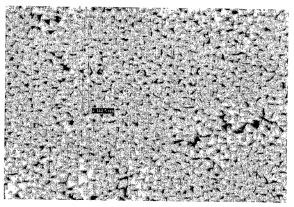
Figure 6 shows a scanning electron micrograph of the Ta coating on the
stainless steel
substrates 22. The substrates 22 were extremely smooth and the surface
roughness
and open structure that result from the coating are clearly visible. Many of
the surface
features have sizes of less than a micron, the very sizes that have been found
effective
for bone and tissue attachment. X-ray diffraction scans of this coating showed
that it
consisted almost entirely of the body centered cubic phase of Ta.
Example 8
In order to study the possibility of using materials other than Ta for porous
coatings,
System 1 was used to deposit TiN on polished stainless steel, which was
located in
position C shown in Figure 2. Two Ti targets 20 were operated at a DC power of
3
kW each. The targets 20 were preconditioned in Ar with the shutter closed for
10.5
minutes. The shutter was then opened and Ti was deposited in Ar only at a
pressure
of 14 mT and gas flow of 1.4 Torr-liters per second. Nitrogen was then
introduced at
a flow rate of 0.6 Torr-liters per second and the pressure rose to 18 mT. The
substrate
had a ¨45 V DC bias applied during the coating, which lasted for a time of 1.5
hours.
Figure 7 shows a scanning electron micrograph of the surface of the TiN
coating that
resulted. It also had a black appearance and the adhesion was excellent. The
similarity between this and the Ta coating is obvious, and demonstrates that a
large
14
WO 2006/004645 CA 02572072 2006-12-27PCT/US2005/022695
number of materials are candidates for producing microscopically rough, porous
surfaces.
While the geometry of a cylindrical magnetron makes oblique incidence coatings
possible in an efficient way, as we have shown, the same results can be
accomplished
using planar targets as well. In the case of planar targets, the requirement
is to place
the substrates 22 far enough from the target surface(s) that a large target-to-
substrate
distance is achieved. Alternatively, the substrates 22 could be placed to the
side of a
planar target 50 so that the material arrives at high incidence angles. This
configuration is illustrated in Figure 8. Of course, the substrate positions
shown in the
case of planar targets make inefficient use of the coating material and
greatly reduce
the deposition rate, which are undesirable from a manufacturing standpoint.
Nevertheless, Figure 8 illustrates how the inventive method could be used with
geometries other than cylindrical magnetrons.
Example 9
We have also discovered that the initial coating conditions can influence the
microstructure and crystalline phase of our coatings while preserving
excellent
adhesion. In one experiment, substrates 22 were loaded in Position C in System
lusing the setup shown in Figure 2 with 34 cm diameter targets 20. With the
shutter
closed, the two Ta targets 20 were operated at 2 kW (1 kW each) at a Kr
pressure of
3.6 mT and a Kr flow of 2.53 Ton-liters per second. After five minutes, and
with the
shutter still closed, a voltage of ¨200 V was applied to the substrates 22 in
order to
plasma clean them. The shutter was opened after five additional minutes and
the
coating was begun with a ¨ 200 V bias still applied to the substrates 22.
These
conditions were maintained for two minutes, at which time the voltage on the
substrates 22 was reduced to ¨ 50 V and the coating was deposited under these
conditions for 180 minutes. There was no flaking evident on these substrates
22.
Except for the initial five minutes of plasma cleaning and two minutes of-200
V bias
sputtering, the conditions in the example above were the same as those used in
Example 7 that produced the structure shown in Figure 6 and the bcc
crystalline
phase. Figure 9 is an atomic force microscope image of the resulting coating
showing
that the microstructure is changed by the initial conditions. While the
features in
15
WO 2006/004645 CA 02572072 2006-12-27PCT/US2005/022695
Figures 6 and 9 are similar and both are microscopically rough, porous
coatings, a
close analysis shows that the structures in Figure 6 are approximately 100 to
200 nm
in size, while those in Figure 9 are about twice as large. Moreover, the X-ray
diffraction pattern shows that the crystalline phase of this coating shown in
Figure 9
was primarily tetragonal, with some bcc present.
Examples 7, 8, and 9 show that both a variety of materials and a variety of
coating
conditions can be used to make the microscopically rough, porous structures we
are
describing.
The combination of a very porous coating and excellent adhesion is very
surprising.
Oblique coating fluxes, thermalized coating atoms and low homologous
temperatures
are known to produce open, columnar coating structures and microscopically
rough
surfaces. However, such coatings typically have very poor adhesion. We have
found
conditions that produce such structures along with excellent adhesion.
An open, porous structure may have other advantages for implantable medical
devices
as well. For example, the microvoids in the coating would permit the
incorporation of
drugs or other materials that could diffuse out over time. Examples are
superoxide
dismutuse to prevent inflammation, proteins to promote bone and tissue growth,
or
other materials that aid in the healing or growth process. In the art, drug-
eluting
coatings on substrates are presently made using polymeric materials. A porous
inorganic coating would allow drug-eluting substrates to be made without
polymeric
overcoats.
The process described in the present invention provides a simple, inexpensive
method
for producing surfaces on implantable devices that aid in their attaclunent to
bone and
tissue. In addition to tantalum and titanium nitride, other coating materials
that could
be used include titanium, molybdenum, zirconium, chromium and other
biocompatible elements. Moreover, it is possible to alter the surface layers
of such
coatings by anodizing or nitriding them or to deposit the oxides or nitrides
of metals
directly.
16
WO 2006/004645 CA 02572072 2006-12-27PCT/US2005/022695
It is also possible to vary the conditions to produce a coating whose
properties change
throughout the thickness. For example, the first part of the coating could be
applied
under conditions that produce a fully dense coating. Then the conditions could
be
changed to those that produce a porous open structure. Such a coating could
provide
corrosion protection for the implant by virtue of the initial dense layer and
good
adhesion to bone through the microscopically rough layer above. In addition,
drugs
that diffuse over time can reside in the pores. Similarly, a nonporous coating
can be
applied to protect the substrate from corrosion. Then, an outer porous layer
can be
applied that easily bonds with animal tissue.
Although the present invention has been described in considerable detail with
reference to certain preferred versions thereof, other versions are possible.
For
example, a substrate can be coated with a layer of a first material and a
layer of a
second, porous material. In another example, the microscopically rough
features can
be bumps instead of pores. The features also may be a combination of bumps and
pores. Therefore, the spirit and scope of the appended claims should not be
limited to
the description of the preferred versions contained herein.
All features disclosed in the specification, including the claims, abstract,
and
drawings, and all the steps in any method or process disclosed, may be
combined in
any combination, except combinations where at least some of such features and
/ or
steps are mutually exclusive. Each feature disclosed in the specification,
including
the claims, abstract, and drawings, can be replaced by alternative features
serving the
same, equivalent or similar purpose, unless expressly stated otherwise. Thus,
unless
expressly stated otherwise, each feature disclosed is one example only of a
generic
series of equivalent or similar features.
Any element in a claim that does not explicitly state "means" for performing a
specified function or "step" for performing a specified function should not be
interpreted as a "means" or "step" clause as specified in 35 U.S.C. 112.
17