Note: Descriptions are shown in the official language in which they were submitted.
CA 02572390 2006-12-22
WO 2006/091221 PCT/US2005/023635
TITLE OF THE INVENTION
[0001] Spectroscopic Methods for Component Particle Analysis
BACKGROUND OF THE INVENTION
[0002] The invention relates generally to the field of hyperspectral analysis
of particle
size, morphology, and spatial distribution.
[0003] Surfaces form the interface between different physical and chemical
entities,
and the physical and chemical processes that occur at surfaces often control
the bulk
behavior of materials. For example, the rate of dissolution of drug particles
in a biological
fluid (e.g., stomach, intestinal, bronchial, or alveolar fluid in a human) can
strongly
influence the rate of uptake of the drug into an animal. Differences in
particle size
distribution between two otherwise identical compositions of the same drug can
lead to
significant differences in the pharmacological properties of the two
compositions. Further
by way of example, the surface area of a solid chemical catalyst can strongly
influence the
number and density of sites available for catalyzing a chemical reaction,
greatly influencing
the properties of the catalyst during the reaction. For these and other
reasons, manufacturers
often try to closely control particle size and shape. Associations between and
among
particles can also affect the pharmacological properties of substances in the
particles, such
as the ability of a substance to dissolve or become active in a biological
system.
[0004] Numerous metliods of analyzing particle sizes and distributions of
particle sizes
are known in the art, including at least optical and electron microscopy,
laser diffraction,
physical size exclusion, dynamic light scattering, polarized light scattering,
mass
spectrometric, sedimentation, focused beam backscattered light reflectance,
iinpedance,
radiofrequency migration, Doppler scattering, and other analytical techniques.
Each of
these techniques has a variety of limitations that preclude its use in certain
situations.
However, all of these techniques share a critical limitation that prevent
effective use of the
techniques for a wide variety of samples for which particle analysis would be
valuable -
namely, none of the prior art techniques is able to distinguish two particles
that differ only
in chemical composition. Put another way, a first particle having
substantially the same
size, shape, and weight as a second particle cannot be distinguished from the
second particle
in these methods. Furthermore, many prior art particle characterization
methods depend on
CA 02572390 2006-12-22
WO 2006/091221 PCT/US2005/023635
serial particle-by-particle analysis and are not suitable for analysis of
multiple particles in
parallel. The present invention overcomes these limitations.
BRIEF SUMMARY OF THE INVENTION
[0005] The invention relates to devices and methods for assessing a geometric
property
of a particle of a substance in a sample, such as a sample in a microscopic
field. Crudely
simplified, the method comprises irradiating the sample, generating a chemical
image of the
sample to identify one or more particles of the substance, and using one or
more image
analysis algorithms to assess the geometric property for the substance. The
chemical image
can, for example, be a Raman, near infrared (NIR), or fluorescent image of the
sample. It is
important the spectroscopic method used to generate the chemical image can
differentiate
the substance of interest from other materials that are or may be present in
the sample. By
way of exaniple, after illuminating the sample, one can generate a chemical
image based on
Raman-shifted radiation scattered by the particle at one or more Raman shift
values
characteristic of the substance. Alternatively, the chemical image of the
sample can be
collected by confocal reflectance NIR imaging at one or more focal planes
within the
sample. Geometric properties of the particles can be used to assess the size
of individual
particles, the size distribution of particles in a population, association of
particles in a
sample, or some combination of these.
[0006] The methods described herein can be used to make two- or three-
dimensional
chemical images of particles of interest, regardless of the presence of other
particles or
compounds in the sample. The methods can be used to simultaneously determine
geometric
properties of multiple particles composed of the same or different materials
in the sample.
The methods can be used to generate time-resolved (i.e., dynamic) chemical
images (e.g.,
video or video-like data) of particles. The methods are highly suitable for
particulate
materials, but can also be used with materials that do not form discrete
particles or materials
which form particles of varying composition.
[0007] In one embodiment, the particle is immobilized prior to generating the
chemical
image and determining the geometrical property(ies). With immobile particles
or particles
suspended in a solid or in a viscous liquid phase, immobilization cail be
unnecessary.
Particles can be immobilized by allowing them to settle or dry on a surface.
Particles can
-2-
CA 02572390 2006-12-22
WO 2006/091221 PCT/US2005/023635
also be immobilized by freezing or otherwise solidifying a liquid suspension
of the particles
on a surface.
[0008] The methods described herein are useful in a wide variety of
applications, such
as in assessing drug particle sizes. By way of example, the sizes of
aerosolized or liquid-
suspended solid particles can be assessed, as can the sizes of one liquid
phase dispersed in
another.
[0009] The invention includes devices for performing such chemical imaging
methods.
For example, in one embodiment, the device uses NIR optimized liquid crystal
(LC)
imaging spectrometer technology for wavelength selection. The NIR optimized
refractive
microscope is used in conjunction with infinity-corrected objectives to form
the NIR image
on the detector with or without the use of a tube lens. An integrated parfocal
analog color
CCD detector provides real-time sample positioning and focusing. The color
image and the
NIR image can be fused using image handling software. In one configuration,
the NIR
microscope is used as a volumetric imaging instrument by imaging substantially
parallel
focal planes through the sample, (i.e., collecting images at varying focal
depths) and
reconstructing a volumetric image of the sample in software. In another
embodiment, the
sample position is fixed and wavelength-dependent depth of penetration is used
in
conjunction with a refractive tube lens to achieve a well characterized
chromatic effect. For
example, the output of the microscope can be coupled to a NIR spectrometer
either via
direct optical coupling or via a fiber optic.
[0010] The invention also includes a chemical imaging addition method in which
the
sample is seeded with a material of known composition, structure, and/or
concentration and
the methods described herein are performed to generate a chemical (e.g., NIR)
image
suitable for qualitative and quantitative analysis.
[0011] Suitable optic platforms for performing the methods described herein
include
microscopes, fiberscopes, macrolens systems, and telescopes, for example.
BRIEF SUMMARY OF THE SEVERAL VIEWS OF THE DRAWINGS
[0012] The patent or application file contains at least one drawing executed
in color.
Copies of this patent or patent application publication with color drawing(s)
will be
provided by the Office upon request and payment of the necessary fee.
-3-
CA 02572390 2006-12-22
WO 2006/091221 PCT/US2005/023635
[0013] Figure 1 depicts Raman spectra acquired from nasal spray samples lE1
(solid
line) and 3E1 (dashed line) in aqueous solution.
[0014] Figure 2 depicts Raman spectra acquired from nasal spray samples lE1
(solid
line) and 3E1 (dashed line) after the samples were allowed to dry on a glass
microscope
slide.
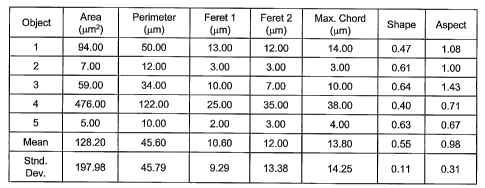
[0015] Figure 3, consisting of Figures 3A, 3B, 3C, and 3D, depicts RCI results
for a
single field of view on the dried lE1 nasal spray sample. Figure 3A depicts a
brightfield
reflectance micrograph of the sample. Figure 3B depicts a polarized light
micrograph of the
sample. Figure 3C depicts a Raman chemical image of the sample. Figure 3D
depicts
Raman spectra corresponding to portions A (solid line in Figure 3D), B (dashed
line in
Figure 3D), and C(alternating solid and dashed line in Figure 3D) of Figure
3C.
[0016] Figure 4 depicts a dispersive Raman spectrum of dextrose illuminated
with 0.4
Watt, 532 nanometer laser light, using a 50x, 0.8 numerical aperture
objective, a 25
micrometer entrance slit, a 0.5 meter spectrometer with 150 grooves per
millimeter, and a 6
second CCD exposure with 5 accumulations.
[0017] Figure 5 depicts a dispersive Raman spectrum of POLYSORBATE (TM) 80
generated using the same spectrometer and settings as in Figure 4.
[0018] Figure 6 depicts a dispersive Raman spectrum of microcrystalline
cellulose
(MCC) generated using the same spectrometer and settings as in Figure 4.
[0019] Figure 7 depicts a dispersive Raman spectrum of carboxymethylcellulose
sodium
(CMC) generated using the same spectrometer and settings as in Figure 4.
[0020] Figure 8 depicts a dispersive Raman spectrum of phenylethyl alcohol
generated
using the same spectrometer and settings as in Figure 4.
[0021] Figure 9 depicts a dispersive Raman spectrum of benzalkonium chloride
generated using the same spectrometer and settings as in Figure 4.
[0022] Figure 10 consists of Figures 10A and l OB. Figure l0A depicts the
chemical
structure of beclomethasone dipropionate (BDP). Figure l OB depicts a
dispersive Raman
spectrum of BDP generated using the same spectrometer and settings as in
Figure 4.
[0023] Figure 11 is the overlaid Raman spectra of Figures 4-10, wherein the
spectra are
indicated with the same line styles as in Figures 4-10.
[0024] Figure 12 consists of Figure 12A, Figure 12B and a particle size
distribution
(PSD) chart (Figure 12C). Figure 12 A depicts a polarized light micrograph of
BDP.
-4-
CA 02572390 2006-12-22
WO 2006/091221 PCT/US2005/023635
Figure 12B is a binarized image of Figure 12A. The PSD chart was prepared by
software
analysis of the binarized image of Figure 12B.
[0025] Figure 13 consists of Figure 13A, Figure 13B and a particle maximum
chord
length distribution graph (Figure 13C). Figures 13A and 13B are replicas of
Figures 12A
and 12B. The graph was prepared by software analysis of the binarized image of
Figure
13B.
[0026] Figure 14, consisting of Figures 14A, 14B, 14C, 14D, and 14E, depicts
results
obtained from RCI of a mixture of BDP and MCC (no water added). Figures 14A
and 14B
are brightfield reflectance and polarized light micrographs, respectively.
Figure 14C is a
color Raman chemical image of the mixture, in which areas A (corresponding to
BDP), B
(corresponding to MCC), and C(corresponding to the background) are indicated.
Figures
14D and 14E are Raman spectra obtained by Raman scattering analysis of regions
A (solid
line), B (dashed line), and C (dotted line) of Figure 14C.
[0027] Figure 15 consists of Figures 15A and' 15B and a PSD data table (Figure
15C).
Figure 15A is a grayscale Raman chemical image assessed at a Raman shift value
characteristic of MCC, and Figure 15B is a binarized image of Figure 15A. The
data in the
PSD table were prepared by software analysis of the binarized image of Figure
15B.
[0028] Figure 16 consists of Figures 16A and 16B and a PSD data table (Figure
16C).
Figure 16A is a grayscale Raman chemical image assessed at a Raman shift value
characteristic of BDP, and Figure 16B is a binarized image of Figure 16A. The
data in the
PSD table were prepared by software analysis of the binarized image of Figure
16B.
[0029] Figure 17, consisting of Figures 17A, 17B, 17C, 17D, and 17E, depicts
results
obtained from RCI of a mixture of BDP and MCC with water added thereto.
Figures 17A
and 17B are brightfield reflectance and polarized light micrographs,
respectively. Figure
17C is a Raman chemical image of the mixture, in which areas A (corresponding
to BDP),
B (corresponding to MCC), and C (corresponding to the background) are
indicated. Figures
17D and 17E are Raman spectra obtained by Raman scattering analysis of regions
A (solid
line), B (dashed line), and C (dotted line) of Figure 17C.
[0030] Figure 18 consists of Figures 18A and 18B and a PSD data table (Figure
18C).
Figure 18A is a grayscale Raman chemical image assessed at a Raman shift value
characteristic of MCC following addition of water, and Figure 18B is a
binarized image of
-5-
CA 02572390 2006-12-22
WO 2006/091221 PCT/US2005/023635
Figure 18A. The data in the PSD table were prepared by software analysis of
the binarized
image of Figure 18.
[0031] Figure 19 consists of Figures 19A and 19B and a PSD data table (Figure
19C).
Figure 19A is a grayscale Raman chemical image assessed at a Raman shift value
,
characteristic of BDP following addition of water, and Figure 19B is a
binarized image of
Figure 19A. The data in the PSD table were prepared by software analysis of
the binarized
image of Figure 19B.
[0032] Figure 20, comprising Figures 20A and 20B depicts a pair of polarized
light
micrographs of the MCC/BDP blend prior to the addition of water (Figure 20A)
and
following addition of water (Figure 20B).
[0033] Figure 21, consisting of Figures 21A, 21B, 21C, 21D, and 21E, depicts
results
obtained from RCI of a sample of BECONASE AQ (TM). Figures 21A and 21B depict
brightfield reflectance and polarized light micrographs, respectively. Figure
21C is a
Raman chemical image of the sample assessed at a Raman shift value
characteristic of BDP.
Figure 21D depicts Raman spectra assessed in several boxed regions of Figure
21B,
including region A, corresponding to BECONASE AQ (TM). Figure 21E depicts
Figures
21 A and 21C overlaid.
[0034] Figure 22 consisting of Figures 22A, 22B, 22C, 22D, and 22E, depicts
results
obtained from RCI of a sample of BECONASE AQ (TM). Figures 22A and 22B depict
brightfield reflectance and polarized light micrographs, respectively. Figure
22C is a
Raman chemical image of the sample assessed at a Raman shift value
characteristic of BDP.
Figure 22D depicts Raman spectra assessed in several boxed regions of Figure
22B,
including region A, corresponding to BECONASE AQ (TM). Figure 22E depicts
Figures
22A and 22C overlaid.
[0035] Figure 23, consisting of Figures 23A, 23B, 23C, 23D, and 23E, depicts
results
obtained from RCI of a sample of BECONASE AQ (TM). Figures 23A and 23B depict
brightfield reflectance and polarized ligllt micrographs, respectively. Figure
23C is a
Raman chemical image of the sample assessed at a Raman shift value
characteristic of BDP.
Figure 23D depicts Raman spectra assessed in several boxed regions of Figure
23B,
including region A, corresponding to BECONASE AQ (TM). Figure 23E depicts
Figures
23A and 23C overlaid.
-6-
CA 02572390 2006-12-22
WO 2006/091221 PCT/US2005/023635
[0036] Figure 24, consisting of Figures 24A, 24B, 24C, 24D, and 24E, depicts
results
obtained from RCI of a sample of a placebo formulated like BECONASE AQ (TM),
but
without BDP. Figures 24A and 24B depict brightfield reflectance and polarized
light
micrographs, respectively. Figure 24C is a Raman chemical image of the sample
assessed
at a Raman shift value characteristic of BDP. Figure 24D depicts Raman spectra
assessed in
several boxed regions of Figure 24B.
[0037] Figure 25, consisting of Figures 25A, 25B, 25C, 25D, and 25E, depicts
results
obtained from RCI of a sample of a placebo formulated like BECONASE AQ (TM),
but
without BDP. Figures 25A and 25B depict brightfield reflectance and polarized
light
micrographs, respectively. Figure 25C is a Raman chemical image of the sample
assessed
at a Raman shift value characteristic of BDP. Figure 25D depicts Raman spectra
assessed in
several boxed regions of Figure 25B.
[0038] Figure 26, consisting of Figures 26A, 26B, 26C, 26D, and 26E, depicts
results
obtained from RCI of a sample of a placebo formulated like BECONASE AQ (TM),
but
without BDP. Figures 26A and 26B depict brightfield reflectance and polarized
light
micrographs, respectively. Figure 26C is a Raman chemical image of the sample
assessed
at a Raman shift value characteristic of BDP. Figure 26D depicts Raman spectra
assessed in
several boxed regions of Figure 26B.
[0039] Figure 27 consists of Figures 27A, 27B, and 27C and a PSD table (Figure
27D).
Figures 27A, 27B, and 27C depict binarized Raman chemical images assessed at a
Raman
shift characteristic of BPD at three regions of interest of the BECONASE AQ
(TM) nasal
spray samples depicted in Figures 21, 22, and 23. The data in the PSD table
were prepared
by software analysis of the binarized image of Figures 27A, 27B, and 27C (ROI
1, ROI 2,
and ROI 3, respectively in the PSD table), and indicated that the mean
particle size was 1.79
+ 1.33 micrometers.
[0040] Figure 28 is a PSD graph which depicts data prepared by software
analysis of the
binarized image of Figures 27A, 27B, and 27C.
[0041] Figures 29 consists of Figures 29A, 29B, and 29C and a particle size
standard
table (Figure 29D). Figure 29A depicts a brightfield reflectance micrograph of
10 micron
NIST-traceable polystyrene microspheres. Figure 29B depicts a Raman chemical
image of
the microspheres, assessed at a Raman chemical shift value characteristic of
polystyrene.
Figure 29C is a color image of Figures 29A and 29B overlaid. The data depicted
in Figure
-7-
CA 02572390 2006-12-22
WO 2006/091221 PCT/US2005/023635
29C were used to determine sphere sizes (maximum chord sizes, in micrometers)
shown in
the table. The table also lists NIST traceable values for the six size
standards assessed. The
spheres indicated with an asterisk in the particle size standard table did not
form arrays.
[0042] Figure 30 is a digital brightfield image of a CdZnTe semiconductor
material
decorated with tellurium inclusions.
[0043] Figure 31 is an NIR microscopic transmittance image of a CdZnTe
semiconductor material decorated with tellurium inclusions.
[0044] Figure 32 consists of Figures 32A, 32B, 32C, and 32D. Figure 32A is a
raw NIR
image frame of a CdZnTe wafer sample. Figure 32B is an NIR image frame of the
sample
of Figure 32A in which the threshold value for the image was set too low.
Figure 32C is an
NIR image frame of the sample of Figure 32A in which the threshold value for
the image
was set too high. Figure 32D is an NIR image frame of the sanlple of Figure
32A in which
the threshold value for the image was set to an intermediate level.
[0045] Figure 33 consists of Figures 33A, 33B, and 33C. Figure 33A is the
original raw
image of four adjacent regions of interest on a CdZnTe wafer. Figure 33B is
the
background-corrected image corresponding to the four adjacent regions of
interest of the
CdZnTe wafer of Figure 33A. Figure 33C is the binarized image corresponding to
the four
adjacent regions of interest of the CdZnTe wafer of Figure 33A.
[0046] Figure 34 is a three-dimensional view of tellurium inclusions in a
CdZnTe wafer.
[0047] Figure 35 is a schematic diagram of a near-infrared (NIR) chemical
imaging
microscope.
[0048] Figure 36 comprises Figures 36A, 36B, 36C, 36D, 36E, and 36F. Figure
36A is
a visual image of an aspirin- and lactose-containing tablet made using a
digital camera. The
dark spot was a locating indicium made with a pen. Figures 36B, 36C, and 36D
are
chemical images of the same tablet, in which lactose-containing portions of
the tablet are
shaded blue and aspirin-containing portions of the tablet are shaded green.
Figure 36C and
36D are NIR and Raman chemical images of the boxed portion of Figure 36B, in
which
aspirin- and lactose-containing regions were differentiated by NIR imaging.
Figures 36B
and 36C were made using the CONDOR (TM) device described herein, and Figure
36D was
made using the FALCON (TM) device described herein. Figure 36E is a comparison
of the
NIR absorption spectra (inverse reflectance plotted against wavelength) of
aspirin (solid
-8-
CA 02572390 2006-12-22
WO 2006/091221 PCT/US2005/023635
line) and lactose (dashed line). Figure 36F is a comparison of the Raman
spectra of aspirin
(solid line) and lactose (dashed line).
[0049] Figure 37 schematically represents an apparatus according to one
embodiment of
the disclosure.
[0050] Figure 38 schematically represent an apparatus according to another
embodiment
of the disclosure.
DETAILED DESCRIPTION OF THE INVENTION
[0051] The invention relates to methods of assessing one or more geometric
properties
of one or more particles of a substance in a sample using a chemical image of
the sample to
identify and characterize the particle(s). The methods are useful, for
example, for assessing
particle sizes and size distributions in mixtures containing both particles of
the substance
and other materials. The methods can also be used to assess association
between
compounds and particles in a sample, such as agglomeration of particles of
different
substances and inclusion of multiple substances in a single particle.
[0052] The present invention is directed to overcoming one or more of the
limitations
inherent to current methods for the determination of geometric properties,
such as particle
size distribution (PSD), for complex mixtures like inhalable pharmaceutical
products.
Restrictions associated with prior art methods for determining PSDs cannot
generate
information for particular molecular species in complex drug formulations.
[0053] The methods described herein relate to methods of assessing geometric
properties (e.g., PSD) of particles of a particular substance (e.g., a single
chemical
compound) in a composition. The methods are not affected by the presence of
particles of
other substances (e.g., pharmaceutical excipients or contaminants) in the
composition. Very
briefly, the methods comprise immobilizing the particles (if necessary),
acquiring chemical
imaging data characteristic of the substance of interest (e.g., Raman, near
infrared (NIR), or
fluorescent chemical image data), and processing that data using image
processing
techniques to describe a geometric property of the particles. Use of image
processing
techniques to quantify geometric properties of particles in an image provides
more precise
and specific information than is obtained by subjective observation of a
microscopic field,
for instance, and permits detailed analysis of the particles in the field. The
methods
described herein have the advantage of being able to determine the identity
and geometric
-9-
CA 02572390 2006-12-22
WO 2006/091221 PCT/US2005/023635
properties of multiple particles substantially simultaneously, even if the
particles are
particles of one or more substances.
[0054] Definitions
[0055] As used herein, each of the following terms has the meaning associated
with it
in this section.
[00561 A "particle of a substance" is an entity having a phase boundary with
one or
more surrounding entities, wherein the entity comprises the substance.
Examples of a
particle of a substance include a solid phase of the substance surrounded by a
liquid or
gaseous phase and a first liquid phase that comprises the substance and is
surrounded by a
second liquid phase that substantially does not comprise the substance. A
particle can
consist entirely or essentially of the substance, or the particle can comprise
other materials.
[0057] "Association" between and among particles refers to agglomeration,
bonding, or
any other close physical (including electrostatic) interaction of two or more
particles,
whether permanent or short-lived.
[0058] A particle is "effectively immobilized" if it is maintained in a
location and an
orientation that do not substantially change during the period of Raman
scattering analysis
described herein.
[0059] The terms "optical" and "spectroscopic" are used interchangeably herein
to refer
to properties of materials (and to methods of assessing such properties). The
term
"spectroscopic" is generally understood to refer to the interaction of
electromagnetic
radiation, electrons, or neutrons with the materials. The term "optical"
typically refers to an
interaction with electromagnetic radiation. For example, although electron
microscopy is
not always commonly considered a "spectroscopic" or "optical" method, the two
terms are
used inclusively herein to encompass electron microscopy and other methods of
assessing
interaction of a material with visible, ultraviolet, or infrared light, with
neutrons, with
electrons, or with other radiation.
[0060] "Spectral resolution" means the ability of a radiation detection system
to resolve
two spectral peaks.
[0061] Two images are combined "in an aligned manner" when the combined image
corresponds at every point to essentially the same point in each of the two
individual
images. Thus, two images of a microscopic field that includes a circle, a
square, and a star
-10-
CA 02572390 2006-12-22
WO 2006/091221 PCT/US2005/023635
are combined in an aligned manner when each of the circle, square, and star of
the two
images of the field overlap essentially precisely in the combined image.
[0062] "Quantification" of a geometric property of a particle means assessment
of the
value of the property with a greater precision than is possible by mere
'visual observation
and estimation of the property at the same level of magnification.
[0063] Detailed Description
[0064] The invention relates to a method of assessing a geometric property of
a particle
of a substance in a microscopic field, or to multiple particles of the same or
different
substances. The method comprises irradiating a particle and generating a
chemical image of
a portion of the field containing the particle (or of the whole field) at one
or more
wavelengths characteristic of the substance. Imaging processing techniques can
be used to
quantify one or more geometric properties of the particle based on the
chemical image.
Such quantified information permits calculation of geometric properties with
far greater
precision than is possible by casual visual analysis of the image alone. By
way of example,
the chemical image can be an image of Raman-shifted light scattered from the
field and
having a wavelength characteristic of Raman-shifted light scattered by the
substance or of
near infrared (NIR) light reflected by the substance. Alternatively, chemical
image can
include multiple characteristic wavelengths (or a characteristic spectrum of
wavelengths) for
the substance. The geometric property can be determined from the chemical
image.
Because chemical image data (e.g., Raman scattering intensities and shift
values or NIR
absorbance/reflectance properties) are characteristic of the compound
elastically scattering,
transmitting, or reflecting the incident radiation, geometric properties of
particles of
differing composition can be assessed in mixtures of such particles.
Furthermore, by
generating a chemical image of an entire field of view, geometric properties
of substantially
all particles in the field can be assessed substantially simultaneously.
[0065] In one embodiment, the devices and methods described herein can be used
to
non-destructively assess semiconductor material defects for the purpose of
increasing
manufacturing yields. For example, the methods have been used as described
herein to
inspect tellurium inclusions in CdZnTe compound semiconductor materials. In
another
einbodiment, the devices and methods described herein can be used to assess
one or more
-11-
CA 02572390 2006-12-22
WO 2006/091221 PCT/US2005/023635
geometric properties of drug- or excipient-containing particles in a
pharmaceutical
composition such as an powdered or tabletted pharmaceutical composition.
[0066] NIR Spectroscopy
[0067] NIR spectroscopy is a mature, non-contact, non-destructive analytical
characterization tool that has wide applicability to a broad range of
materials. The NIR
region of the electromagnetic spectrum encompasses radiation with wavelengths
of 0.78 to
2.5 micrometers (i.e., radiation with wavenumbers of 12,800 to 4,000 inverse
centimeters,
i.e., 12,800 to 4,000 cm-1). NIR spectra result from the overtone and
combination bands of
fundamental mid-infrared (MIR) bands.
[0068] NIR-based spectroscopy can be used to rapidly obtain both qualitative
and
quantitative compositional information about the molecular makeup of a
material. Optical
imaging (e.g., digital optical imaging) yields spatial information about a
material, such as
the morphology, topography, and location in an imaged field. By combining the
spatial
information obtained by optical imaging and the compositional information
obtained by
NIR spectroscopy, a chemical image can be generated in which the chemical
makeup of a
material in a field of view can be mapped in two or three (if desired) spatial
dimensions.
This combination, designated NIR chemical imaging, combines NIR spectroscopy
and
optical imaging for molecule-specific analysis of materials. An NIR chemical
imaging
microscope apparatus useful for materials characterization is described
herein.
[0069] NIR microscopes can be used to obtain NIR absorption, emission,
transmittance,
reflectance, or elastic scattering data at a single wavelength or over a
spectrum of
wavelengths, typically for samples ranging in size between 1 and 1000
micrometers. NIR
microscopes are typically equipped with a visible light camera for visual
location of a
region of interest on a sample. After focusing the microscope on the desired
location, the
sample is illuminated with NIR radiation from a spectrometer, such as a
Fourier transform
(FT) spectrometer. Reflective optics are used to direct the transmitted,
reflected, or
elastically scattered light from the sample to a NIR detector. NIR absorption
data (e.g., a
spectrum) can be collected in transmittance, scattering, or reflectance mode.
[0070] NIR imaging cameras have been used by other prior to this disclosure.
By using
optical filters (e.g., cold filters) to block visible wavelengths (ca. 0.4 to
0.78 micrometers),
charge-coupled devices (CCDs, such as those used in digital cameras and
camcorders) can
-12-
CA 02572390 2006-12-22
WO 2006/091221 PCT/US2005/023635
be used to sense NIR light to wavelengths around 1100 nanometers. Other
regions of the
NIR spectrum can be viewed using devices such as indium gallium arsenide
(InGaAs; ca.
0.9 to 1.7 micrometers) and indium antimonide (InSb; ca. 1.0 to 5.0
micrometers) focal
plane array (FPA) detectors. Integrated wavelength N1R imaging allow study of
relative
light intensities of materials over broad ranges of the NIR spectrum. However,
useful
chemical image information is unattainable without some type of discrete
wavelength
filtering device.
[0071] The use of dielectric interference filters in combination with NIR FPAs
is one
method in which N1R chemical information can be obtained from a sample. To
form an
NIl2 chemical image, a NIR light beam is defocused to illuminate a wide field
of view and
the reflected, transmitted, or elastically scattered light from the
illuminated area is imaged
onto a two-dimensional NIR detector. A selection of discrete dielectric
interference filters
(provided in a filter wheel or in a linearly- or circularly-variable format)
can be positioned
in front of a broadband NIR light source, or in front of the NIR FPA (i.e.,
between the
illuminated area and the FPA) in order to collect NIR wavelength-resolved
images.
Typically, the use of several fixed bandpass filters is required to access the
entire NIR
spectrum. The spatial resolution of the NIR image approaches that of the
optical
microscope, and spectral resolution of several nanometers has been
demonstrated. Key
limitations of the dielectric filter approach include the need for a multitude
of discrete filters
to provide appreciable free spectral range, and the reliance on moving
mechanical parts in
continuously tunable dielectric interference filters as a requirement to form
wavelength-
resolved images. Although moving mechanical assemblies can be engineered, they
add
significant cost and complexity to NIR chemical imaging systems. Alternatives
to moving
mechanical assemblies can be more cost effective and provide performance
advantages.
[0072] Acousto-optic tunable filters (AOTFs) have been employed in NIR imaging
spectrometers with substantially no moving parts. The AOTF is a solid-state
device that is
capable of filtering wavelengths from the UV to the mid-IR bands, depending on
the choice
of the filter's crystal material. Operation of an AOTF is based on interaction
of light with a
traveling acoustic sound wave in an anisotropic crystal medium. Incident light
is diffracted
with a narrow spectral bandpass when a radio frequency signal is applied to
the device. By
changing the applied radio frequency (which can be under computer control, for
example),
the spectral passband can be tuned rapidly and without moving parts.
-13-
CA 02572390 2006-12-22
WO 2006/091221 PCT/US2005/023635
[0073] AOTFs have limitations that limit their usefulness for NIR chemical
imaging.
For example, AOTF imaging performance is degraded appreciably from diffraction-
limited
conditions due to dispersion effects and image shifting effects. Furthermore,
AOTFs exhibit
temperature instability and non-linear properties that complicate their use in
imaging
spectrometers.
[0074] NIR microspectroscopic imaging performed since the development of the
first
NIR microprobes has involved spatial scanning of samples beneath an NIR
microscope in
order to construct an NIR "map" of a surface. In point-by-point scanning
methods
performed using an NIl2 microscope, the NIR light beam is focused onto the
surface of a
sample or apertured to illuminate a small region of a sample and a spectrum is
collected
from each spatial position. Images are obtained by rastering the sample
through the focused
or apertured NIR light beam and the spectra recorded are then reconstructed to
form an
image. Although point scanning can be used to produce an image based on NIR
contrast,
long experimental times are required, because the duration of data collection
is proportional
to the number of image pixels. As a result, point-scanned images exhibit low
image
definition, which limits usefulness of the technique for routine assessment of
material
morphology. The spatial resolution of a point-scanned image is limited by the
size of the
NIR illumination spot on the sample (i.e., not less than 1 micrometer) and by
the rastering
mechanism, which requires the use of moving mechanical parts that are
challenging to
operate reproducibly.
[0075] The NIIZ chemical imaging devices and methods described herein exhibit
high
spatial and spectral resolution, the spatial resolution being essentially
diffraction-limited and
the spectral resolution being limited substantially only by the resolution of
the spectrometer
used to resolve the light provided to the sample (or collected from the
sample, depending on
the configuration of the device used). Favorable spectral resolution can be
achieved, for
instance, using a liquid crystal (LC) imaging spectrometer.
[0076] In general, LC devices provide diffraction-limited spatial resolution.
The
spectral resolution of the LC imaging spectrometer is comparable to that
achieved using
dispersive monochromator and Fourier transform interferometers. In addition,
LC
technology provides high out-of-band rejection, broad free spectral range,
moderate
transmittance, high overall light throughput (i.e., etendue or geometric
capacity to transmit
radiation), and highly reproducible random access computer controlled tuning.
-14-
CA 02572390 2006-12-22
WO 2006/091221 PCT/US2005/023635
[0077] LC imaging spectrometers allow N]R chemical images of samples to be
recorded
at discrete wavelengths (i.e., photon energies). A spectrum can be generated
for thousands
of spatial locations on a sample surface by tuning the LC imaging spectrometer
over a range
of wavelengths and collecting NIR images at each of the locations. Contrast
can be
generated in the images based on the relative amounts of NIR absorption,
transmittance,
reflectance, or elastic scattering that is generated by the different species
located throughout
the sample. An image generated in this manner is one embodiment of a chemical
image
disclosed herein. Since a high quality NIR spectrum can be generated for each
pixel
location, a wide variety of chemometric analysis tools, both univariate and
multivariate, can
be applied to the NIR image data to extract pertinent information. The
resulting image can
be displayed in numerous formats, including tabulated numeric data, two- and
three-
dimensional graphs, and static and time-resolved video images.
[0078] Correlative multivariate routines can be applied to chemical images
collected
from samples intentionally seeded with a known standard material. This
approach
incorporates calibration standards within an image field of view and permits
quantitative
chemical image analysis. Digital image analysis procedures can also be applied
to high
image quality chemical images to perform routine particle analysis in two or
three spatial
dimensions. Volumetric (i.e., three-dimensional) chemical image analysis can
be performed
using numerical deconvolution computational strategies, for example.
[0079] Raman Spectroscopy
[0080] Raman spectroscopy provides information about the vibrational state of
molecules. Many molecules have atomic bonds capable of existing in a number of
vibrational states. Such a molecule is able to absorb incident radiation that
matches a
transition between two of its allowed vibrational states and to subsequently
emit the
radiation. Most often, absorbed radiation is re-radiated at the same
wavelength, a process
designated Rayleigh or elastic scattering. In some instances, the re-radiated
radiation can
contain slightly more or slightly less energy than the absorbed radiation
(depending on the
allowable vibrational states and the initial and final vibrational states of
the molecule). The
result of the energy difference between the incident and re-radiated radiation
is manifested
as a shift in the wavelength between the incident and re-radiated radiation,
and the degree of
difference is designated the Raman shift (RS), measured in units of wavenumber
(inverse
-15-
CA 02572390 2006-12-22
WO 2006/091221 PCT/US2005/023635
length). If the incident light is substantially monochromatic (single
wavelength) as it is
when using a laser source, the scattered light which differs in frequency can
be more easily
distinguished from the Rayleigh scattered light.
[0081] Because Raman spectroscopy is based on irradiation of a sample and
detection of
scattered radiation, it can be employed non-invasively and non-destructively,
such that it is
suitable for analysis of biological samples in situ. Thus, little or no sample
preparation is
required. In addition, water exhibits very little Raman scattering, and Raman
spectroscopy
techniques can be readily performed in aqueous environments.
[0082] The Raman spectrum of a material can reveal the molecular composition
of the
material, including the specific functional groups present in organic and
inorganic
molecules. Raman spectroscopy is useful for detection of pharmaceutical and
other
chemical agents because most, if not all, of these agents exhibit
characteristic 'fingerprint'
Raman spectra, subject to various selection rules, by which the agent can be
identified.
Raman peak position, peak shape, and adherence to selection rules can be used
to determine
molecular identity and to determine conformational information (e.g.,
crystalline phase,
degree of order, strain, grain size) for solid materials.
[0083] In the past several years, a number of key technologies have been
introduced into
wide use that have enabled scientists to largely overcome the problems
inherent to Raman
spectroscopy. These technologies include high efficiency solid-state lasers,
efficient laser
rejection filters, and silicon CCD detectors. In general, the wavelength and
bandwidth of
light used to illuminate the sample is not critical, so long as the other
optical elements of the
system operate in the same spectral range as the light source.
[0084] In order to detect Raman scattered light and to accurately determine
the Raman
shift of that light, the sample should be irradiated with substantially
monochromatic light,
such as light having a bandwidth not greater than about 1.3 nanometers, and
preferably not
greater than 1.0, 0.50, or 0.25 nanometer. Suitable sources include various
lasers and
polychromatic light source-monochromator combinations. It is recognized that
the
bandwidth of the irradiating light, the resolution of the wavelength resolving
element(s), and
the spectral range of the detector determine how well a spectral feature can
be observed,
detected, or distinguished from other spectral features. The combined
properties of these
elements (i.e., the light source, the filter, grating, or other mechanism used
to distinguish
Raman scattered light by wavelength) define the spectral resolution of the
Raman signal
-16-
CA 02572390 2006-12-22
WO 2006/091221 PCT/US2005/023635
detection system. The known relationships of these elements enable the skilled
artisan to
select appropriate components in readily calculable ways. Limitations in
spectral resolution
of the system (e.g., limitations relating to the bandwidth of irradiating
light, grating groove
density, slit width, interferometer stepping, and other factors) can limit the
ability to resolve,
detect, or distinguish spectral features. The skilled artisan understands that
and how the
separation and shape of Raman scattering signals can determine the acceptable
limits of
spectral resolution for the system for any of the Raman spectral features
described herein.
[0085] Chemicallmaging
[0086] Spectroscopic methods can be used in chemical imaging (also known as
spectroscopic imaging) techniques through the use of imaging spectrometers
such as liquid
crystal imaging spectrometers. The development of this technology in recent
years has
enabled widefield spectroscopic imaging to develop and mature. Chemical
imaging is a
versatile technique suitable for analysis of complex heterogeneous materials.
Applications
of chemical imaging range from the analysis of polymer blends, defect status
analysis in
semiconductor materials, inclusions in human breast tissue, characterization
of corrosion
samples and detection, classification and identification of biological and
chemical warfare
agents. Chemical imaging provides a potential solution for obtaining both
qualitative and
quantitative image information about molecular composition and morphology
materials
allowing a more accurate and more rapid analysis than traditional imaging or
'wet' chemical
methods.
[0087] Ordinary optical imagery of the sample can be obtained using a mirror,
beamsplitter, or prism arrangement inserted into the turret wheel of the
microscope by
collecting an image with an analog or digital color or monochrome charge-
coupled device
(CCD) or CMOS detector.
[0088] Chemical image data can be collected using the Raman-based or NIR-based
spectroscopic methods described herein. Alternatively, chemical image data can
be
generated using other spectroscopic methods such as such as luminescence or
absorbance,
reflectance, or transmittance spectroscopy or energy dispersive spectrometry.
Raman and
NIR-based chemical imaging methods are preferred, owing to the significant
amount of =
chemical identity information that can ordinarily be extracted from Raman
scattering and
NIR absorbance/transmission/elastic scattering characteristics of a material.
However,
-17-
CA 02572390 2006-12-22
WO 2006/091221 PCT/US2005/023635
substantially any spectroscopic method that can distinguish a material of
interest from other
materials in a sample can'be used in the methods described herein.
[0089] Optical image data and chemical image data can be fused, using software
for
example. In spectroscopic imaging mode, the magnified spectroscopic image is
coupled
through a liquid crystal imaging spectrometer and collected on a detector
appropriate for the
selected chemical imaging method (e.g., a Si CCD detector for RCI). A central
processing
unit, such a PENTIUM (TM, Intel Corporation) processor-based computer, is used
for
spectroscopic image collection and processing. The optical image detector
(e.g., an analog
color CCD), the chemical image detector (e.g., a Si CCD), an automated XYZ
translational
microscope stage (controlled by way of a controller), and a liquid crystal
imaging
spectrometer (controlled by way of a liquid crystal imaging spectrometer
controller) can be
cooperatively operated with commercial software, such as the CHEMAQUIRE (TM;
ChemImage Corporation, Pittsburgh, PA) or CHEMIMAGE XPERT (TM; ChemImage
Corporation, Pittsburgh, PA) software packages, either alone or in conjunction
with image
processing software such as the CHEMANALYZE (TM; Chemlmage Corporation,
Pittsburgh, PA) software package.
[0090] Although chemical imaging and visible light cameras often generate
images
having differing contrast, the sample fields of view can be matched using one
or both of
optical and software manipulations. The chemical and optical images can be
compared or
fused using overlay and correlation techniques to produce a near-real time
view of both
detector outputs on a single computer display. Comparative and integrated
views of the
sample can enhance understanding of sample morphology and architecture. By
comparing
the optical and chemical images, useful information can be acquired about the
chemical
composition, structure, and concentration of samples.
[0091] Dispersive spectroscopy data can be collected simultaneously with
collection of
chemical imaging data. By introducing a polarization sensitive beam splitting
element in
the optical path prior to the liquid crystal imaging spectrometer, a portion
of the signal from
the sample may be coupled to a renlote dispersive spectrometer. The signal can
be coupled
directly (i.e., by direct optical coupling) or using a fiber optic cable, for
example.
Conventional spectroscopic tools can thereby be used to gather spectra for
traditional, high-
speed spectral analysis. The spectrometers can be any of a fixed filter
spectrometer, a
-18-
CA 02572390 2006-12-22
WO 2006/091221 PCT/US2005/023635
grating-based spectrometer, a Fourier transform spectrometer, and an acousto-
optic
spectrometer, for example.
[0092] Preferably, liquid crystal (LC) imaging spectrometer technology is used
for
chemical image wavelength selection. The LC imaging spectrometer can, for
example, be
one of a Lyot liquid crystal tunable filter (LCTF), an Evans Split-Element
LCTF, a Solc
LCTF, a ferroelectric LCTF, a liquid crystal Fabry Perot (LCFP), a hybrid
filter that
combines two or more of the above-mentioned LC filter types, and one of the
above
mentioned filter types in combination with fixed bandpass and bandreject
filters, which can
be of the dielectric, rugate, holographic, color absorption, acousto-optic or
polarization filter
types.
[0093] A chemical imaging microscope can be used as a volumetric imaging
instrument
by moving the sample through focus in the Z-axial dimension, collecting images
in- and
out-of-focus, and reconstructing a volumetric image of the sample in software.
For samples
having some volume (e.g., bulk materials, surfaces, interfaces, interphases),
volumetric
chemical imaging has been shown to be useful for failure analysis, product
development,
and routine quality monitoring. Quantitative analysis can be performed
simultaneously with
volumetric analysis. Volumetric imaging can be performed in a non-contact mode
without
modifying the sample using numerical confocal techniques, which require that
the sample
be imaged at discrete focal planes. The resulting images are processed,
reconstructed, and
visualized. Computational optical sectioning reconstruction techniques based
on a variety
of strategies have been demonstrated, including nearest neighbors and
iterative
deconvolution, and substantially any of these known methods can be used in
connection
with the devices and methods described herein.
[0094] An alternative to combining sample positioning with computation
reconstruction
is to employ a tube lens in the image formation path of the microscope which
introduces
chromatic aberration. As a result the sample can be interrogated as a function
of sample
depth by operating the LC imaging spectrometer and collecting images at
different
wavelengths which penetrate to differing degrees into bulk materials. These
wavelength-
dependent (i.e., depth-dependent) images can be reconstructed to form
volumetric images of
materials without requiring the sample to be moved by applying computational
optical
sectioning reconstruction algorithms.
-19-
CA 02572390 2006-12-22
WO 2006/091221 PCT/US2005/023635
[0095] Chemical Image Addition Calibration
[0096] A chemical imaging addition method (CIAM) can be used to calibrate or
otherwise analyze samples. CIAMs involve seeding a sample with a material of
known
composition, structure, and/or concentration and thereafter generating a
chemical image
suitable for qualitative and quantitative analysis. A standard calibration
curve can be
constructed, which is a plot of analytical response for a particular technique
as a function of
known analyte concentration. By measuring the analytical response from an
unknown
sample, an estimate of the analyte concentration can then be interpolated or
extrapolated
from the calibration curve. For example, when the analytical response is
linearly (i.e., direct
proportionally) related to concentration, the concentration of the unknown
analyte can be
determined by plotting the analytical response from a series of standards and
interpolating
or extrapolating the unknown concentration from the line. When an analyte
exhibits a linear
analytical response to increasing concentration, addition of known amounts of
the analyte to
a sample that contains an unknown amount of the analyte permits determination
of the
amount of analyte present prior to the additions (i.e., in the original
sample). Similar
methods can be used to determine an unknown analyte concentration by
comparison with a
curve that fits analytic responses that are not directly proportional to
standard analyte
concentrations. The primary advantage of CIAMs is that the matrix remains
constant for all
samples.
[0097] CIAMs can be used for qualitative and quantitative analysis. CIAMs can
use
one or more spatially isolated analyte standards to calibrate the chemical
imaging response
obtained, from portions of a sample at which the standard is not present.
Chemical imaging
can generate in parallel thousands of linearly independent, spatially-resolved
spectra of
analytes in a sample that may or may not include complex matrices. These
spectra can be
processed to generate unique contrast intrinsic to a desired analyte species
without the use
of stains, dyes, or contrast agents. Calibration using a standard can be used
to correlate the
contrast with the amount of the analyte present.
[0098] CIAMs can involve several data processing steps, typically including,
but not
limited to:
[0099] 1. Ratiometric correction, performed by dividing the sample chemical
image by
the background chemical image to produce a result having a floating point data
type.
-20-
CA 02572390 2006-12-22
WO 2006/091221 PCT/US2005/023635
[0100] 2. Normalizing the divided image by dividing each intensity value at
every pixel
in the image by the vector norm for its corresponding pixel spectrum. The
vector norm is
the square root of the sum of the squares of pixel intensity values for each
pixel spectrum.
Normalization is applied for qualitative analysis of chemical images. For
quantitative
analysis, normalization is not employed, but can instead rely on the use of
partial least
squares regression (PLSR) techniques.
[0101] 3. Correlation analysis, including Euclidian distance and cosine
correlation
analysis (CCA), which are established multivariate image analysis techniques
that assess
similarity in spectral image data while simultaneously suppressing background
effects.
More specifically, CCA assesses chemical heterogeneity without the need for
training sets,
identifies differences in spectral shape and efficiently provides chemical
image-based
contrast that is independent of absolute intensity. The CCA algorithm treats
each pixel
spectrum as a projected vector in n-dimensional space, where n is the number
of
wavelengths sampled in the image. An orthonormal basis set of vectors is
chosen as the set
of reference vectors and the cosine of the angles between each pixel spectrum
vector and the
reference vectors are calculated. The intensity values displayed in the
resulting CCA
images are these cosine values, where a cosine value of 1 indicates the pixel
spectrum and
reference spectrum are identical, and a cosine value of 0 indicates the pixel
spectrum and
the reference spectrum are orthogonal (no correlation). The dimensions of the
resulting
CCA image is the same as the original image because the orthonormal basis set
provides n
reference vectors, resulting in n CCA images.
[0102] 4. Principal component analysis (PCA) is a data space dimensionality-
reduction
technique. A least squares fit is drawn through the maximum variance in the n-
dimensional
data set. The vector resulting from this least squares fit is termed the first
principal
component (PC) or the first loading. After subtracting the variance explained
from the first
PC, the operation is repeated and the second principal component is
calculated. This
process is repeated until some percentage (normally 95% or greater) of the
total variance in
the data space is explained. PC score images can then be visualized to reveal
orthogonal
information including sample information, as well as instrument response,
including noise.
Reconstruction of spectral dimension data can be performed, guided by cluster
analysis,
including without PCs that describe material or instrument parameters that one
desires to
amplify or suppress, depending on the needs of the sensing application.
-21-
CA 02572390 2006-12-22
WO 2006/091221 PCT/US2005/023635
[0103] Until recently, seamless integration of spectral analysis, chemometric
analysis
and digital image analysis has not been commercially available. Individual
communities
have independently developed advanced software applicable to their specific
requirements.
For example, digital imaging software packages that treat single-frame gray-
scale images
and spectral processing programs that apply chemometric techniques have both
reached a
relatively mature state. One limitation to the development of chemical
imaging, however,
has been the lack of integrated software that combines enough of the features
of each of
these individual disciplines to have practical utility.
[0104] Historically, practitioners of chemical imaging were forced to develop
their own
software routines to perform each of the key steps of the data analysis.
Typically, routines
were prototyped using packages that supported scripting capability, such as
Matlab, IDL,
Grams or LabView. These packages, while flexible, are limited by steep
learning curves,
computational inefficiencies, and the need for individual practitioners to
develop their own
graphical user interface (GUI). Today, commercially available software does
exist that
provides efficient data processing and the ease of use of a simple GUI.
[0105] Software that meets these goals must address the entirety of the
chemical
imaging process. The chemical imaging analysis cycle illustrates the steps
needed to
successfully extract information from chemical images and to tap the full
potential provided
by chemical imaging systems. The cycle begins with the selection of sample
measurement
strategies and continues through to the presentation of a measurement
solution. The first
step is the collection of images. The related software must accommodate the
full
complement of chemical image acquisition configurations, including support of
various
spectroscopic techniques, the associated spectrometers and imaging detectors,
and the
sampling flexibility required by differing sample sizes and collection times.
Ideally, even
relatively disparate instrument designs can have one intuitive GUI to
facilitate ease of use
and ease of adoption.
[0106] The second step in the analysis cycle is data preprocessing. In
general,
preprocessing steps attempt to minimize contributions from chemical imaging
instrument
response that are not related to variations in the chemical composition of the
imaged sample.
Some of the functionalities needed include: correction for detector response,
including
variations in detector quantum efficiency, bad detector pixels and cosmic
events; variation
in source illumination intensity across the sample; and gross differentiation
between spectral
-22-
CA 02572390 2006-12-22
WO 2006/091221 PCT/US2005/023635
lineshapes based on baseline fitting and subtraction. Examples of tools
available for
preprocessing include ratiometric correction of detector pixel response;
spectral operatioris
such as Fourier filters and other spectral filters, normalization, mean
centering, baseline
correction, and smoothing; spatial operations such as cosmic filtering, low-
pass filters, high-
pass filters, and a number of other spatial filters.
[0107] Once instrument response has been suppressed, qualitative processing
can be
employed. Qualitative chemical image analysis attempts to address a simple
question,
"What is present and how is it distributed?" Many chemometric tools fall under
this
category. A partial list includes: correlation techniques such as cosine
correlation and
Euclidean distance correlation; classification techniques such as principal
components
analysis, cluster analysis, discriminant analysis, and multi-way analysis; and
spectral
deconvolution techniques such as SIMPLISMA, linear spectral unmixing and
multivariate
curve resolution.
[0108] Quantitative analysis deals with the development of concentration map
images.
Just as in quantitative spectral analysis, a number of multivariate
chemometric techniques
can be used to build the calibration models. In applying quantitative chemical
imaging, all
of the challenges experienced in non-imaging spectral analysis are present in
quantitative
chemical imaging, such as the selection of the calibration set and the
verification of the
model. However, in chemical imaging additional challenges exist, such as
variations in
sample thickness and the variability of multiple detector elements, to name a
few.
Depending on the quality of the models developed, the results can range from
semi-
quantitative concentration maps to rigorous quantitative measurements.
[0109] Results obtained from preprocessing, qualitative analysis and
quantitative
analysis must be visualized. Software tools must provide scaling, automapping,
pseudo-
color image representation, surface maps, volumetric representation, and
multiple modes of
presentation such as single image frame views, montage views, and animation of
multidimensional chemical images, as well as a variety of digital image
analysis algorithms
for look up table (LUT) manipulation and contrast enhancement.
[0110] Once digital chemical images have been generated, traditional digital
image
analysis can be applied. For example, Spatial Analysis and Chemical Image
Measurement
involve binarization of the high bit depth (typically 32 bits/pixel) chemical
image using
threshold and segmentation strategies. Once binary images have been generated,
analysis
-23-
CA 02572390 2006-12-22
WO 2006/091221 PCT/US2005/023635
tools can examine a number of image domain features such as size, location,
alignment,
shape factors, domain count, domain density, and classification of domains
based on any of
the selected features. Results of these calculations can be used to develop
key quantitative
image parameters that can be used to characterize materials.
[0111] The final category of tools, Automated Image Processing, involves the
automation of key steps or of the entire chemical image analysis process. For
example, the
detection of well defined features in an image can be completely automated and
the results
of these automated analyses can be tabulated based on any number of criteria
(particle size,
shape, chemical composition, etc). Automated chemical imaging platforms have
been
developed that can run for hours in an unsupervised fashion.
[0112] This invention incorporates a comprehensive analysis approach that
allows user's
to carefully plan experiments and optimize instrument parameters and should
allow the
maximum amount of information to be extracted from chemical images so that the
user can
make intelligent decisions.
[0113] Raman-Based Chemical Imaging System
[0114] Raman chemical imaging (RCI) combines Raman spectroscopy with digital
imaging for molecular-specific analysis of materials. This technology allows
images of
sainples to be constructed by recording Raman scattered light at discrete
wavelengths
emanating from defined locations in an illuminated sample. A spectrum is
generated
corresponding to millions of spatial locations at the sample surface by tuning
the liquid
crystal imaging Raman spectrometer over a range of wavelengths and collecting
images
intermittently. Depending on the materials, depth-related information can also
be obtained
by using different excitation wavelengths or by capturing Raman chemical
images at
incremental planes of focus. Contrast is generated in the images based on the
relative
amounts of Raman scatter that is generated by the different species located
throughout the
sample. Since a Raman spectrum is generated for each pixel location,
univariate and/or
multivariate (i.e., chemometric) analysis tools such as correlation analysis,
Principal
Component Analysis (PCA), and factor rotation, including Multivariate Curve
Resolution
(MCR), can be applied to the image data to extract pertinent information.
[0115] A spatial resolving power of approximately 250 nanometers has been
demonstrated for Raman chemical imaging using laser illumination at visible
wavelengths.
-24-
CA 02572390 2006-12-22
WO 2006/091221 PCT/US2005/023635
This is almost two orders of magnitude better than infrared imaging that is
typically limited
to a spatial resolution of about 20 microns, owing to diffraction. In
addition, image
definition (based on the total number of imaging pixels) can be very high for
RCI based on
liquid crystal optics because high pixel density detectors (often 1 million or
more detector
elements per detector) can be used. The wavelength of light used for
illumination is not
critical and can be in the range from 220 to 1100 nanometer.
[0116] An apparatus for Raman chemical imaging has been described by Treado in
U.S.
Patent number 6,002,476, and in U.S. patent application 09/619,371, filed 19
July 2000,
which are incorporated herein by reference. Other descriptions of Raman
chemical imaging
are U.S. patent application 09/800,953, filed 7 March 2001; U.S. patent
application
09/976,391, filed 21 October 2001; U.S. patent application 10/185,090, filed
27 June 2002;
U.S. patent application 10/184,580 filed 27 June 2002; U.S. provisional patent
application
60/144,518, filed 19 July 1999; U.S. provisional patent application
60/347,806, filed 10
January 2002; U.S. provisional patent application 60/144,518, filed 19 July
1999; U.S.
provisional patent application 60/187,560, filed 28 March 2000; U.S.
provisional patent
application 60/239,969, filed 13 November 2000; U.S. provisional patent
application
60/301,708 filed, 28 June 2001; and U.S. provisional patent application
60/422,604, filed 21
November 2002. Each of the foregoing patents and applications is incorporated
herein by
reference.
[0117] RCI instrument configurations can include platforms based on a RCI
microscope, for example. An example of a commercially available device which
is suitable
for use in the methods described herein is a laboratory or transportable field
Raman
microscope such as the FALCON Raman microscope (TM; Chemlmage Corporation,
Pittsburgh, PA).
[0118] An RCI microscope such as the FALCON (TM) system described above
combines in a single platform a solid state laser for sample excitation, a
refractive optical
microscope base, which is equipped with infinity-corrected microscope
objectives, an
automated XYZ translational microscope stage, and a quartz tungsten halogen
(QTH) lamp
and/or a mercury (Hg) lamp. Also a part of the microscope system is an analog
color
charge-coupled device (CCD) detector for ordinary optical image collection and
digital
image collection, a liquid crystal imaging spectrometer for spectroscopic
image wavelength
selection, a thermoelectrically cooled (TE) Si CCD detector for Raman chemical
image
-25-
CA 02572390 2006-12-22
WO 2006/091221 PCT/US2005/023635
capture, and a remote, dispersive monochromator equipped with a CCD detector
for
dispersive spectral collection.
[0119] NIR-Based Chemical Imaging System
[0120] The NIR chemical imaging microscope combines in a single platform a NIR
optimized refractive optical microscope base, which is equipped with NIR
optimized
infinity-corrected microscope objectives, an automated XYZ translational
microscope stage
and quartz tungsten halogen (QTH) lamps to secure and illuminate samples for
NIR
spectroscopy and imaging, an analog color charge-coupled device (CCD) detector
for
ordinary optical image collection and digital image collection, a NIR LC
imaging
spectrometer for NIR chemical image wavelength selection and a room
temperature or
optionally cooled NIR FPA for NIR image capture.
[0121] Figure 35 is a schematic diagram of the NIR chemical imaging
microscope. NIR
illumination is directed to the sample in a reflected light configuration
using a QTH source
or other broadband white light source, including metal halide or Xe arc lamps
1 or a
transmitted light configuration using QTH or suitable NIR source 2 of an NIR
optimized
refractive optical microscope platform 3. The reflected or transmitted NIR
light is collected
from the sample positioned on the automated XYZ translational microscope stage
4 through
an infinity-corrected NIR optimized microscope objective S.
[0122] Ordinary optical imagery of the sample can be obtained using a mirror
or
beamsplitter or prism arrangement inserted into turret 6 and collecting an
image with an
analog or digital color or monochrome charge-coupled device (CCD) or CMOS
detector 7.
In NIR chemical imaging mode, the magnified NIR image is coupled through a NIR
LC
imaging spectrometer 8 and collected on a room temperature or cooled NIR focal
plane
array (FPA) detector 9. The FPA is typically comprised of indium gallium
arsenide
(InGaAs), but may be comprised of other NIR sensitive materials, including
platinum
silicide (PtSi), indium antimonide (InSb) or mercury cadmium telluride
(HgCdTe). Using a
beamsplitting element inserted into turret 6, NIR and ordinary optical imagery
can be
collected with an analog monochrome or color CCD detector 7 and NIR FPA 9
simultaneously.
[0123] A central processing unit 10, typically a Pentium computer, is used for
NIR
chemical image collection and processing. The analog color CCD 7, NIR FPA 9,
automated
-26-
CA 02572390 2006-12-22
WO 2006/091221 PCT/US2005/023635
XYZ translational microscope stage 4 controlled via a controller 12 and NIR LC
imaging
spectrometer 8 (through LC imaging spectrometer controller 11) are operated
with
commercial software, such as Acquisition Manager (Chemlmage Corporation,
Pittsburg,
PA; previously known as Chemlcon, Inc.) in conjunction with ChemImage
(ChemImage
Corporation, Pittsburg, PA; previously known as ChemIcon, Inc.).
[0124] By introducing a polarization sensitive beam splitting element in the
optical path
prior to the NIR LC imaging spectrometer 8 (not shown in schematic diagram), a
portion of
the NIR light from the sample may be coupled to a remote NIR spectrometer
(also not
shown in schematic diagram).
[0125] Preferably, NIR optimized liquid crystal (LC) imaging spectrometer
technology
is used for wavelength selection. The LC imaging spectrometer may be of the
following
types: Lyot liquid crystal tunable filter (LCTF); Evans Split-Element LCTF;
Solc LCTF;
Ferroelectric LCTF; Liquid crystal Fabry Perot (LCFP); or a hybrid filter
technology
comprised of a conlbination of the above-mentioned LC filter types or the
above mentioned
filter types in combination with fixed bandpass and bandreject filters
comprised of
dielectric, rugate, holographic, color absorption, acousto-optic or
polarization types.
[0126] One novel component of this invention, is that a NIR optimized
refractive
microscope is used in conjunction with infinity-corrected objectives to form
the NIR image
on the detector without the use of a tube lens. The microscope can be
optimized for NIR
operation through inherent design of objective and associated anti-reflective
coatings,
condenser and light source. To simultaneously provide high numerical apertures
the
objective should be refractive. To minimize chromatic aberration, maximize
throughput and
reduce cost the conventional tube lens can be eliminated, while having the NIR
objective
form the NIR image directly onto the NIR focal plane array (FPA) detector,
typically of the
InGaAs type. The FPA can also be comprised of Si, SiGe, PtSi, InSb, HgCdTe,
PdSi, Ge,
analog vidicon types. The FPA output is digitized using an analog or digital
frame grabber
approach.
[0127] An integrated parfocal analog CCD detector provides real-time sample
positioning and focusing. An analog video camera sensitive to visible
radiation, typically a
color or monochrome CCD detector, but may be comprised of a CMOS type, is
positioned
parfocal with the NIR FPA detector to facilitate sample positioning and
focusing without
-27-
CA 02572390 2006-12-22
WO 2006/091221 PCT/US2005/023635
requiring direct viewing of the sample through conventional eyepieces. The
video camera
output is typically digitized using a frame grabber approach.
[0128] Particle Analysis Method
[0129] Analysis of particles of a composition identifiable by chemical imaging
analysis
is performed by collecting chemical image data from sample particles, such as
substantially
immobilized sample particles. From the spectroscopic imaging data, a chemical
image is
generated at one or more spectroscopic values characteristic of the component
of interest to
yield a two- or three-dimensional image of the spatial distribution of the
component. By
way of example, suitable spectroscopic values include Raman shift values, NIR
absorption
wavelengths, or NIR reflectance wavelengths. The image is subjected to any of
a variety of
known univariate and/or multivariate image processing techniques that are
known in the art
in order to determine at least one geometric property of the component
particles. Such
geometric properties can be used to describe the properties of the component
particles in the
sample.
[0130] If desired, an optical or spectroscopic image of the field of view is
made at
substantially the same time as the chemical image data are collected (or at
least near enough
in time that the particles in the field have not substantially moved). A
dispersive chemical
image of the entire field can also be collected. Because the geometric
property(ies) are
calculated from chemical image data at a spectroscopic value (e.g., the
wavenumber
corresponding to a characteristic Raman shift value or a wavelength of NIR
radiation
characteristically reflected by the substance) characteristic of the substance
of interest (or at
two or more such characteristic values), the presence of other substances or
particles in the
sample does not affect assessment of the particles of interest, at least so
long as the other
substance(s) or particle(s) do not exhibit the same or indistinguishable
spectral properties.
Two substances with similar spectral properties can be distinguished, for
example, by
concentrating analysis on a region of the corresponding spectrum in which the
two
substances differ more than in other regions of the spectrum. An optical or
spectroscopic
image of the field can indicate the presence, extent, and geometric properties
of particles of
components other than the substance of interest in the composition that is
analyzed.
[0131] The present methods have the advantage, relative to prior optical
microscopy
methods, that spectral information that can unambiguously identify the
composition of
-28-
CA 02572390 2006-12-22
WO 2006/091221 PCT/US2005/023635
particles can be collected simultaneously with optical information relating to
particle size
and shape. Furthermore, because the spectral methods described herein can be
used to
collect spectral information characteristic of multiple compounds, prior
optically-based
methods of assessing particle geometry can be applied on a compound-by-
compound basis
to a sample containing a mixture of compounds. The spectral methods described
herein can
distinguish a particle of a first pure substance from a particle of a second
pure substance,
and can also distinguish these particles from particles of mixed composition.
The methods
can also be used to map the relative amounts of multi-component particles in
different
regions of a single particle (e.g., a particle formed by agglomeration of
multiple particles of
differing composition).
[0132] Sample Immobilization
[0133] In one embodiment, the present invention requires effective
inunobilization of
the substance of interest on a substrate having properties conducive to the
relevant chemical
imaging method to be used (e.g., a Raman inactive substrate when Raman
chemical imaging
is to be performed). Such a substrate should preferably be flat, resistant to
damage or
modification upon illumination, resistant to thernlal expansion, relatively
spectrally inactive,
and non-interferent with the radiation scattered from, absorbed by, or
reflected from the
sample.
[0134] For Raman chemical imaging applications, an appropriate choice of
substrate is
an aluminum-coated glass microscope slide. Suitable substrates for NIR and
other
spectroscopic modalities are also known in the art. Ordinary glass microscope
slides can
also be used, at least with certain laser illumination wavelengths that are
apparent to skilled
artisans and/or readily empirically determined. Powdered or aerosolized
particles or
particles suspended in a liquid can be applied to surface of such a slide and
any liquid in the
composition can be allowed to dry. Alternatively, compositions in which the
particles of
interest are suspended in a fluid can be frozen on the surface of a slide
(e.g., by cooling the
slide and spraying an aerosolized particle suspension thereon). As another
alternative, a
composition comprising particles of interest can be suspended in a polymer
resin that is
thereafter cured to immobilize the particles. The resin can be cured in place
or sliced after
curing. Monolithic solids (e.g., tablets, caplets, and lozenges) can be simply
placed on a
surface or secured in place.
-29-
CA 02572390 2006-12-22
WO 2006/091221 PCT/US2005/023635
[0135] If a liquid preparation of particles (e.g., solid particles suspended
in liquid or a
particulate liquid phase suspended in a continuous liquid phase) is to be
analyzed, the
preparation can be immobilized by maintaining a thin layer of the liquid under
conditions
(e.g., high humidity for aqueous preparations) in which the liquid will not
evaporate.
Alternatively, liquid samples can be sandwiched between transparent glass or
plastic slides,
optionally having a spacer interposed between the slides to yield a liquid
layer of defined
thickness.
[0136] Chemical imaging can also be performed on non-immobilized particles.
With
non-immobilized particles, it is important to take into account the time
required for
chemical image data analysis and to limit the period of data acquisition to a
period in which
movement of the particles is either minimal or recorded. In instances in which
chemical
imaging data can be rapidly collected (e.g., when Raman scattered light is
collected at one
or a small number of RS values), particle motion can be disregarded. In such
instances,
serial collection of chemical image data sets can be used to assess dynamic
changes (e.g.,
agglomeration, evaporation, precipitation, or adhesion) in a sample of
particles. In instances
in which a greater amount of chemical image data i,s to be collected and
particle movement
may be significant during the period of data collection, one or more
techniques for
correlating the location of moving particles witll data collection must be
used (e.g., optical
sighting methods). Such methods are known in the art.
[0137] RCI Data Collection
[0138] RCI data can be collected using known methods. For example, a
commercially
available FALCON RCI microscope (TM; ChemImage Corporation, Pittsburgh, PA)
can be
used according to the manufacturer's instructions.
[0139] In order to ensure proper peak positions in dispersive Raman and RCI
data, the
RCI instrument should be calibrated using a NIST-accepted calibration standard
for Raman
spectrometers. A common standard is acetaminophen. If the identity(ies) of
components of
the sample other than the substance of interest are known, then Raman spectral
data for each
of those components can be generated. This information permits identification
of
appropriate portions of the Raman spectrum to scan during RCI data acquisition
to avoid
overlapping Raman scattering peaks.
-30-
CA 02572390 2006-12-22
WO 2006/091221 PCT/US2005/023635
[0140] Typically, a Raman peak that both is distinctive of the substance of
interest and
exhibits an acceptable signal-to-noise ratio will be selected. Multiple Raman
shift values
characteristic of the substance can be assessed, as can the shape of a Raman
spectral region
that may include multiple Raman peaks. If the sample includes unknown
components, then
the entire Raman spectrum can be scanned during RCI data acquisition, so that
the
contributions of any contaminants to the data can be assessed.
[0141] In order to collect RCI data, substantially immobilized particles are
brought into
focus under the microscope and the appropriate data collection parameters for
the
instrument are set. Raman chemical image(s) are collected. Brightfield and
other
supporting optical imagery can also be acquired at this time to provide
complimentary
spatial/birefringence information in addition to the RCI data.
[0142] NIR Chemical Image Data Collection
[0143] NIR chemical image data can be collected using known methods. For
example,
a commercially available FALCON (TM; Chemlmage Corporation, Pittsburgh, PA)
chemical imaging microscope can be used according to the manufacturer's
instructions.
[0144] In order to ensure proper peak positions in NIR chemical image data,
the
instrument should be calibrated using a calibration standard having known NIR
absorption,
elastic scattering, or reflection peaks. If the identity(ies) of components of
the sample other
than the substance of interest are known, then NIR spectral data for each of
those
components can be generated. This information permits identification of
appropriate
portions of the infrared spectrum to scan during chemical image data
acquisition to avoid
overlapping peaks.
[0145] Typically, an NIR spectral peak that both is distinctive of the
substance of
interest and exhibits an acceptable signal-to-noise ratio will be selected.
Multiple
wavelength values characteristic of the substance can be assessed, as can the
shape of an
NIR absorption or reflection spectral region that may include multiple peaks.
If the sample
includes unknown components, then the entire NIR or infrared spectrum can be
scanned
during data acquisition, so that the contributions of any contaminants to the
data can be
assessed.
[0146] In order to collect NIR spectral data, substantially immobilized
particles are
brought into focus under the microscope and appropriate data collection
parameters for the
-31-
CA 02572390 2006-12-22
WO 2006/091221 PCT/US2005/023635
instrument are set. NIR chemical image(s) are collected. Brightfield and other
supporting
optical imagery can also be acquired at this time to provide complimentary
spatial/birefringence information in addition to the NIR data.
[0147] Data processing
[0148] Acquired chemical images are subjected to one or more univariate and/or
multivariate image processing strategies. Many image processing strategies are
described in
the art, and selection of one or more such strategies is within the level of
ordinary skill in
this field. Various software packages are also commercially available which
are able to
translate two- and three-dimensional chemical data sets geometric properties
for particles.
An example of suitable software for use with the FALCON (TM) chemical imaging
microscope system is the CHEMIMAGE XPERT (TM) software package available from
ChemImage Corporation (Pittsburgh, PA).
[0149] A useful method for creating an easily-manipulated image which can be
used for
geometric property determination is creation from chemical imaging data of one
or more
binary image frames, each corresponding to a particular characteristic
spectral value and/or
a particular plane of focus. For example, software can be used to assign a
value of "1" to
pixels that contain spatial/spectral information characteristic of the
substance of interest and
a value of "0" to pixels containing spatial/spectral information not
characteristic of the
substance. Once chemical images have been binarized, appropriate particle
sizing software
is applied to the processed data to determine molecule-specific particle
sizes.
[0150] Typical geometrical parameters that are used to describe particle size
based on
two-dimensional data include the following: Area (cross-sectional area of
particle);
Perimeter (boundary length of particle); Feret diameter 1 (horizontal distance
across
particle); Feret diameter 2 (vertical distance across particle - i.e., Feret
diameter along axis
perpendicular to Feret diameter 1); Max chord length (maximum distance across
particle);
Shape factor (i.e., the value of the formula (4 x pi x Area) / Perimeter~2);
Aspect ratio (Feret
diatneter 1/ Feret diameter 2).
[0151] Typical geometrical parameters that are used to describe particle size
based on
three-dimensional data include the following: Volume (volume of the particle);
Surface
area (surface of the particle); Feret diameters (three, orthogonal to one
another); Maximum
' -32-
CA 02572390 2006-12-22
WO 2006/091221 PCT/US2005/023635
chord length (maximum distance across particle); various shape factors, and
various
measures of aspect ratios or sphericity of the particle.
[0152] These geometrical parameters can be determined using the methods
described
herein or calculated from geometrical parameters that can be determined using
such
methods.
[0153] The dimensional limits of the particle analysis methods described
herein are
defined by the chemical imaging system being used. Currently, the minimum
spatial
differentiation limit of the Chemlmage FALCON (TM) chemical imaging microscope
is
believed to be about 200-250 nanometers, meaning that geometrical properties
of particles
smaller than this could not be effectively assessed using that system. The
theoretical lower
limit to the size of particles that can be assessed using these methods is on
the order of the
diffraction limit of the incident light (taking into account known
deconvolution techniques,
which may lower the limit further). The methods described herein can be
readily applied to
any new instrument having a lower spatial differentiation limit than the
FALCON (TM)
device.
[0154] System and Method for Dynamic Chemical Imaging
[0155] The methods described in this section can be performed using a system
or
method for detecting dynamic changes that occur in a sample between a first
time interval
and a second time interval using a series of at least first and second
sequential chemical
images of the sample. The first chemical image corresponds to an image of the
sample
during a first time interval. The second chemical image corresponds to an
image of the
sample at a second time interval after the first time interval. Such methods
can be useful for
assessing time-dependent changes in component particle position, composition,
or both, for
example.
[0156] During the first time interval: (i) the sample is illuminated with a
plurality of
photons to thereby produce photons scattered or emitted by the sample; (ii) a
two-
dimensional array of detection elements is then used to simultaneously detect
scattered or
emitted photons in a first predetermined wavelength band from different
locations on or
within the sample; and (iii) the two-dimensional array of detection elements
is thereafter
used one or more further times to simultaneously detect scattered or emitted
photons in one
or more further predetermined wavelength band(s) from different locations on
or within the
-33-
CA 02572390 2006-12-22
WO 2006/091221 PCT/US2005/023635
sample. The outputs of the two-dimensional array of detection elements during
the first
time interval are then combined to generate the first chemical image of the
sample.
[0157] During the second time interval: (i) the sample is illuminated with a
plurality of
photons to thereby produce photons scattered or emitted by the sample; (ii)
the two-
dimensional array of detection elements is then used to simultaneously detect
scattered or
emitted photons in a first predetermined wavelength band from different
locations on or
within the sample; and (iii) the two-dimensional array of detection elements
is thereafter
used one or more further times to simultaneously detect scattered or emitted
photons in one
or more further predetermined wavelength band(s) from different locations on
or within the
sample. The outputs of the two-dimensional array of detection elements during
the second
time interval are then combined to generate the second chemical image of the
sample.
[0158] Dynamic changes occurring in the sample between the first time interval
and the
second time interval are detected based on one or more differences between the
first and
second chemical images.
[0159] The present invention permits rapid observation of the sample with full
spatial
information, and allows the monitoring of the evolution and changes in the
sample that are
naturally proceeding or occurring (i.e., under equilibrium conditions,) as
well as those that
are additionally forced or imposed by creating a non-equilibrium condition via
an external
means (e.g., one or more external fields or forces applied to the sample). In
certain
embodiments, the external means may be applied to a specific location within
the sample
(rather than the whole sample).
[0160] Figure 37 schematically represents an apparatus according to one
embodiment of
the disclosure. The apparatus shown in Figure 37 enables providing a high
optical
throughput for imaging low light levels at variable magnification. Referring
to Figure 37,
sample 100 is positioned on substrate 105. Substrate 105 can be any
conventional
microscopic slide or other means for receiving and optionally securing sample
100. Light
source 110 is positioned to provide incident light to sample 100. Light source
110 can
include any conventional photon source, including laser, LED, and other IR or
near IR
devices. Light source 110 may also be selected to provide evanescence
illumination of the
sainple. In one embodiment, the bandwidth of the source is in the range of
about 15-25
cm l
-34-
CA 02572390 2006-12-22
WO 2006/091221 PCT/US2005/023635
[0161] Referring still to Figure 37, it should be noted that light source 110
is positioned
to provide incident light at an angle to sample 100 as opposed to light
shining orthogonal to
sample 100. In other words, the radiation used to illuminate the sample need
not pass
through the optical train of a conventional microscope (or macroscope);
rather, it can
illuminate the sample at an oblique angle from above or below sample 100.
Photon beam
112 is received and deflected by mirror 115 through lens 120. Lens 120 may
optionally be
used to focus the light on sample 100. Alternatively, the photon beam 112 may
be directed
towards the sample 100 without the need for the mirror 115.
[0162] The multitude of photons in beam 112 reaching sample 100 illuminate the
sample and are either scattered or absorbed by the sample, which can result in
subsequent
emission (luminescence) at different wavelengths. As known to those skilled in
the art, the
term "luminescence" includes a wide range of optical processes described using
other
names. These include: fluorescence, phosphorescence, photoluminescence,
electroluminescence, chemiluminescence, sonoluminescence, thermoluminescence
and even
up-conversion. Scattered photons are schematically represented as beams 116
and 118
while specularly reflected photons are represented schematically as beam 114.
Luminescently-emitted photons are also represented as beam 118. Optical lens
125 is
positioned to receive photon beams 116 and 118. Optical lens 125 may be used
for
gathering and focusing received photon beams. This includes gathering and
focusing both
polarized and non-polarized photons. In general, the sample size determines
the choice of
light gathering optical lens 125. For example, a microscope lens may be
employed for
analysis of the sub-micron to micrometer specimens. For larger samples, macro
lenses can
be used. Optical lens 125 (as well as lens 120) may include a simple reduced
resolution/aberration lens with a larger numerical aperture to thereby
increase system's
optical throughput and efficiency. Mirror 130 is positioned to direct emitted
or scattered
photon beams 118 to tunable filter 140. It should be noted that placement of
mirror 130 is
optional and may be unnecessary in configurations where tunable filter is
positioned above
sample 100.
[0163] Laser rejection filter 135 may be positioned prior to tunable filter
140 to filter
out scattered illumination light represented by beam 116 and to optimize the
performance of
the system. In other words, rejection filter 135 enables spectrally filtering
of the photons at
the illuminating wavelength.
-35-
CA 02572390 2006-12-22
WO 2006/091221 PCT/US2005/023635
[0164] A conventional tunable filter (including electro-optical, mechanical,
or other
tunable filter) can be used to further the principles of the disclosure.
Examples of suitable
tunable filters include an liquid crystal tunable filter ("LCTF") or an
acousto-optical tunable
filter ("AOTF"). The electro-optical filters (or other tunable filters) allow
specific
wavelengths or ranges of wavelengths of light to pass through as an image,
depending on
the control signals placed on the device by a controller. The wavelengths that
can be passed
through tunable filter 140 may range from 200 nanometers (ultraviolet) to 2000
nanometers
(i.e., the far infrared). The choice of wavelength depends on the desired
optical region
and/or the nature of the sample being analyzed.
[0165] Image sensor 145 may be a digital device such as for example a two-
dimensional, image focal plane array ("FPA") or CCD or CMOS sensor. The
optical region
employed to characterize the sample of interest governs the choice of FPA
detector. For
example, a two-dimensional array of silicon charge-coupled device ("CCD")
detection
elements, can be employed with visible wavelength fluorescence and Raman
spectroscopic,
while gallium arsenide (GaAs) and gallium indium arsenide (GaInAs) FPA
detectors can be
employed for image analyses at near infrared wavelengths. The choice of such
devices
depends on the type of sample being analyzed. In one embodiment, each
detection element
in the two-dimensional array of detection elements used to form image sensor
145 functions
to detect photons scattered or emitted from a different spatial location on or
within the
sample. In one embodiment, image sensor 145 produces digital images of the
entire view of
the sample as processed by tunable filter 140.
[0166] Figure 38 schematically represents an apparatus according to another
embodiment of the disclosure. More specifically, Figure 38 schematically shows
a high
optical throughput configuration for imaging low light levels at variable
magnification. The
collection of optics are similar to that illustrated in Figure 37 but with
illumination from the
underside of sample 100.
[0167] It is noted that in both Figures 37 and 38, sample 100 is illuminated
at an oblique
angle. Specifically referring to Figure 38, photonic beam 120 and the plane
axis of sample
100 define an oblique angle. It has been found that through oblique
illumination, a so-called
"Dark Field Raman Imaging" is developed. As opposed to the conventional bright
field
Raman configuration, the dark field Raman imaging decouples the image capture
optics
from the delivery of exciting radiation. Consequently, internal scattering and
attenuation of
-36-
CA 02572390 2006-12-22
WO 2006/091221 PCT/US2005/023635
the incident radiation has been minimized to improve the signal-to-noise (S/N)
ratio. Also,
the location of the optical source external to the optical train further
allows the use of a
lower cost, less powerful illumination source as well as enables a simpler,
less expensive
integration of several illumination sources into the system. The application
of this
configuration is not limited to Raman and luminescence imaging and can be
successfully
used, for example, with conventional spectroscopy.
[0168] In each of the embodiments shown in Figures 37 and 38, a computer or
processor
(not shown in the figures) can be coupled to and used to control the optical
devices
including light source (110), lenses (120, 125, 135), mirrors (115, 130) and
tunable filter
(140). The computer is also coupled to image sensor 145 and functions to
generate
"chemical images" from the output of the image sensor 145. In one embodiment,
each
chemical image is a spatially accurate wavelength-resolved image of the sample
that is
formed from multiple "frames"; wherein each frame has plural spatial
dimensions and is
created from photons of a particular wavelength (or wave number) or from
photons in a
particular wavelength band (or wave number band) that are collected
simultaneously by
image sensor 145 from different spatial locations on or within sample 100. In
each
chemical image, multiple frames may be combined to form a complete image
across all
wavelengths (wave numbers) of interest. The chemical images generated by the
computer
may be further analyzed by the computer and/or displayed to a user.
[0169] The present invention uses an apparatus such as those shown in Figures
37 and
38 to detect dynamic changes that occur in sample 100 between a first time
interval and a
second subsequent time interval using a series of at least first and second
sequential
chemical images of sample 100.
[0170] During the first time interval: (i) sample 100 is illuminated with
photons from
source 110 to thereby produce photons scattered or emitted by sample 100; (ii)
image sensor
145 is then used to simultaneously detect scattered or emitted photons in a
first
predetermined wavelength band (selected by tunable filter 140) from different
locations on
or within the sample; and (iii) for each of one or more further predetermined
wavelength
band(s) (each of which is sequentially selected using tunable filter 140),
image sensor 145 is
thereafter used to simultaneously detect scattered or emitted photons from
different
locations on or within the sample. The outputs of detector 1450 (for each of
the
wavelengths or wavelength bands selected by tunable filter 140 during the
first time
-37-
CA 02572390 2006-12-22
WO 2006/091221 PCT/US2005/023635
interval) are then combined by a computer (not shown in the figures) to
generate the first
chemical image of the sample.
[0171] During the second subsequent time interval: (i) sample 100 is
illuminated with
photons from source 110 to thereby produce photons scattered or emitted by
sample 100;
(ii) image sensor 145 is then used to simultaneously detect scattered or
emitted photons in a
first predetermined wavelength band (selected by tunable filter 140) from
different locations
on or within the sample; and (iii) for each of one or more further
predetermined wavelength
band(s) (each of which is sequentially selected using tunable filter 140),
image sensor 145 is
thereafter used to simultaneously detect scattered or emitted photons from
different
locations on or within the sample. The outputs of detector 145 (for each of
the wavelengths
or wavelength bands selected by tunable filter 140 during the first time
interval) are then
combined by the computer to generate the second chemical image of the sample.
[0172] Dynamic changes occurring in the sample between the first time interval
and the
second time interval are detected based on one or more differences between the
first and
second chemical images. Computer analysis of the chemical image with or
without the
physical image may be used to detect (or enhance detection of) the dynamic
changes. The
dynamic changes may also be detected by a user viewing a display of the
chemical images.
[0173] In various embodiments, a series of many sequential chemical images are
obtained rapidly in succession to generate a "movie" of the sample. For
example, as many
as 100 chemical images per second of the sample may be obtained in order to
detect
dynamic changes in the sample in substantially real-time. In some embodiments,
the
temporal resolution of the chemical images in the sequence may be as fine a 1
millisecond,
i.e., the system will generate a chemical image of the sample every
millisecond. Other
temporal resolutions can also be selected including, for example, a temporal
resolution that
equates to chemical images spaced apart by as much as 15 minutes between
adjacent
images. When using the present invention to monitor a particular process or
reaction, the
temporal resolution selected should be sufficient to detect dynamic changes of
interest that
occur in the sample over time.
[0174] The present invention thus permits rapid observation of sample 100 with
full
spatial information, and allows the monitoring of the evolution and changes in
sample 100
that are natural proceeding or occurring (i.e., under equilibrium conditions),
as well as those
that are additionally forced or imposed by creating a non-equilibrium
condition via an
-38-
CA 02572390 2006-12-22
WO 2006/091221 PCT/US2005/023635
external means (e.g., one or more external fields or forces applied to the
sample). In certain
embodiments, the external means are applied to a specific location within
sample 100
(rather than to the whole sample). Examples of samples that may be analyzed
and observed
used the dynamic chemical imaging techniques of the present invention includes
biological
samples or micro-fluidic circuits undergoing changes over time. These changes
may
include displacement, chemical interaction, a change in chemical state, phase
change,
growth, sluinkage, chemical decomposition, chemical metabolism and physical
strain.
Numerous other examples of samples/changes applicable to the present invention
will be
recognized by the those skilled in the art and are considered within the scope
of the present
invention.
[0175] As noted above, the present invention may be used to detect dynamic
changes in
the sample that result from application of an external condition to the
sample. Such external
conditions include, for example, varying an electric or magnetic field applied
to or within
sample 100 between the first and second time intervals; varying an external
optical field
applied to or within the sample between the first and second time intervals,
wherein the
external optical field is distinct from the optical field initially used to
illuminate the sample;
varying the optical field applied to or within the sample between the first
and second time
intervals, wherein the additional optical field is produced by pulsing the
optical filed used to
illuminate the sample; varying internally generated pho,tons applied to or
within the sanlple
between the first and second time intervals; varying a polarization used to
illuminate the
sample between the first and second time intervals; varying a temperature of
the sample
between the first and second time intervals; varying a pressure applied to the
sample
between the first and second time intervals; or varying a stress applied to or
within the
sample between the first and second time intervals. In other embodiments, a
chemical
gradient associated with the sample (e.g., a chemical gradient imposed on the
sample) varies
between the first and second time intervals. In still further embodiments, a
physiological or
biological stress is induced in the sample between the first and second time
intervals. In
another important embodiment, the dynamic effect of adding one or more
chemical species
(e.g., a pharmaceutically active agent, an antibody, or a nucleic acid) to a
sample is
observed at multiple times.
[0176] In some embodiments, each chemical image in the sequence is made up of
multiple separate spatially accurate wavelength-resolved images of the sample
(each of
-39-
CA 02572390 2006-12-22
WO 2006/091221 PCT/US2005/023635
which is formed from multiple "frames" as discussed above), wherein each of
the multiple
separate spatially accurate wavelength-resolved images corresponds to one of a
plurality of
different depths within the sample. These embodiments are useful for detecting
chemical
changes occurring throughout the volume of sample 100, rather than changes
occurring on a
single surface or plane of the sample.
[0177] In still further embodiments, differences between or among various
chemical
images in the sequence may be correlated (using, e.g., the computer discussed
above or by a
user) with orthogonal (i.e., complementary) measurements of the sample made
during each
of the time intervals associated with the sequence, in order to enhance
detection or
observation of dynamic changes in the sample. Examples of orthogonal
measurements that
may be used include measurements made using the following modalities: Raman
scattering,
near infrared absorption (NIR), visual imagery, video or luminescence. Other
orthogonal
measurements may also be used and are considered to be within the scope of the
present
invention.
[0178] Multiple Particle Analyses
[0179] If the composition being analyzed comprises particles having
distinguishable
spectral properties, then the particle analytical methods described herein can
be used to
assess geometric properties of all of the spectrally-distinguishable types of
particles in the
composition. By way of example, if an aerosolized pharmaceutical composition
contains
two particle types that can be differentiated by their Raman scattering peaks,
then RCI data
can be collected at two or more Raman shift values - one Raman shift value
characteristic of
one particle type, and another Raman shift value characteristic of the other
particle type.
The two particle types can be differentiated by assessing multiple Raman
scattering
properties (e.g., scattering at multiple RS values) characteristic of each of
the particles. This
RCI data set will include information sufficient to describe geometric
properties of both
particle types.
[0180] Combinations of spectral properties can be used to describe geometric
properties
of particles that cannot be identified by a single characteristic spectral
characteristic. By
way of example, if the composition described in the previous paragraph
contains a third
particle type which can be differentiated from all other components of the
composition by a
characteristic fluorescence peak, then geometric properties of that third
particle type can be
-40-
CA 02572390 2006-12-22
WO 2006/091221 PCT/US2005/023635
assessed by analysis of fluorescent imaging data obtained for the
characteristically-
fluorescing particle. Combinations of spectroscopic properties of a material
(e.g.,
absorbance of visible, infrared, or near-infrared light; reflectance or
polarization properties;
shape or texture deduced from a microscopy technique such as scanning electron
microscopy; Raman scattering behavior, such as a characteristic Raman shift
value; or
elemental content, such as assessed using energy dispersive spectroscopy) can
also be used
to identify a particle type.
[0181] If all particle types except one in a composition can be characterized
by a single
spectroscopic characteristic, then all particles that do not exhibit that
characteristic can be
presumed to be the remaining particle type, and optical microscopy data can be
used in
combination with chemical imaging data to assess one or more geometric
properties of the
remaining particle type. In some instances, the chemical identity of particles
other than
those of a particular compound is not important and need not be determined,
other than to
confirn-i the absence of the particular compound in those particles.
[0182] Examples
[0183] The invention is now described with reference to the following
Examples. These
Examples are provided for the purpose of illustration only, and the invention
is not limited
to these Examples, but rather encompasses all variations which are evident as
a result of the
teaching provided herein.
[0184] Example 1
[0185] RCI Assessment of Nasal Spray Preparation
[0186] In this example, a nasal spray preparation was used which contained
beclomethasone dipropionate (BDP) as an active pharmaceutical agent and the
following
components as inactive agents: microcrystalline cellulose (MCC);
carboxymethylcellulose
sodium (CMC); dextrose; benzalkonium chloride; POLYSORBATE 80 (TM); and
phenylethyl alcohol.
[0187] Figures 1 and 2 depict Raman spectra obtained using two batches
(designated
lEl and 3E1) of the nasal spray preparation. The Raman spectra shown in Figure
1 were
obtained after applying the batches to individual slides and assessing the
spectra while the
preparation remained wet. The spectra in Figure 2 were obtained after applying
the same
-41-
CA 02572390 2006-12-22
WO 2006/091221 PCT/US2005/023635
batches to individual slides and assessing the spectra after the preparation
had dried. The
improved peak sharpness discernable in the spectra of Figure 2 is believed to
be attributable,
at least in part, to the greater immobilization of the components of the dried
preparations.
[0188] Figure 3 depicts brightfield and polarized light micrographs (Figures
3A and 3B,
respectively) and a Raman chemical image (Figure 3C) of the dried batch 1E1 on
a slide.
The Raman spectra of regions A, B, and C of Figure 3C are shown in Figure 3D
and
indicate that components of the preparation can be distinguished by their
Raman spectral
properties.
[0189] Figures 4 through 11 depict Raman spectra obtained for each component
of the
nasal spray preparation, assessed as individual pure components. In Figure 11,
the Raman
spectra of the pure components are overlaid to show that each component has at
least one
Raman spectral property by which it can be distinguished from the other
components of the
sample.
[0190] Figures 12 and 13 depict a polarized light micrograph and a
corresponding
binarized image of micronized BDP and geometric properties calculated for 31
particles
calculated from the binarized image using a commercial software package. The
mean BDP
particle size was determined to be 3.02 3.16 micrometers in diameter. The
PSD is shown
graphically in Figure 13.
[0191] Figures 14 through 16 relate to experiments performed with a blend of
micronized BDP and MCC in the dry state. The sample was prepared by placing a
mixture
of BDP and MCC (approximately 20:80 BDP:MCC by volume) on a glass microscope
slide.
It is expected that the crude nature of the sample preparation resulted in
formation of
relatively large aggregates of BDP and MCC.
[0192] Figure 14 depicts brightfield reflectance image and polarized light
images
(Figures 14A and 14B, respectively) and a composite Raman chemical image
(Figure 14C)
of the BDP/MCC mixture. The polarized light image reveals the birefringent
nature of both
components in the mixture. The channels of the composite Raman chemical image
corresponding to BDP (1 in Figures 14C through 14E) and MCC (2 in Figures 14C
through
14E) are indicated. These results indicate that BDP and MCC domains and
background
areas (3 in Figures 14C through 14E) exhibit characteristic Raman spectral
signatures.
[0193] Figure 15 shows a grayscale Raman image (Figure 15A), a binary image
(Figure
15B) and PSD table associated with the MCC aggregates in the field of view.
Due to the
-42-
CA 02572390 2006-12-22
WO 2006/091221 PCT/US2005/023635
large aggregate in the field of view surrounded by several, much smaller
aggregates, the
average MCC "particle" (more likely an agglomerate) size was 33.91 71.45
micrometers.
[0194] Figure 16 shows a grayscale Raman image (Figure 16A), a binary image
(Figure
16B) and a PSD table associated with the BDP aggregates in the field of view.
The average
BDP "particle" (inore likely an agglomerate) size was determined to be 36.99
19.27
micrometers. These results illustrate the ability of the technology to
differentiate and
identify a drug substance from excipients and the utility of the software to
assess particle
size of individual domains that exist in the field of view.
[0195] Figures 17 through 19 demonstrate the ability of these methods to
identify drug
substance and determine particle size and PSD of drug substance in a blend of
micronized
BDP and MCC following the addition of water. A small aliquot (approximately 10
microliters) of distilled water was introduced into the dry BDP/MCC mixture
used in the
experiments corresponding to Figures 14 through 16 using a microsyringe
manually guided
while viewing through the FALCON Microscope with the CCD video camera.
Manually
controlling delivery of the water to the sample on a microscope scale was
challenging. The
addition of water caused particles to move out of the field of view while new
ones moved
into the field of view, which made it difficult to make an accurate comparison
of particle
statistics before and after the addition of water.
[0196] Figure 17 shows a brightfield reflectance image (Figure 17A), a
polarized light
image (Figure 17B), and a composite Rainan chemical image (Figure 17C) of the
BDP/MCC mixture following addition of water. The green and blue color channels
of the
composite Raman chemical image have been color-coded for BDP and MCC,
respectively.
The channels of the composite Raman chemical image corresponding to BDP (1 in
Figures
17C through 17E) and MCC (2 in Figures 17C through 17E) are indicated. These
results
indicate that BDP and MCC domains and background areas (3 in Figures 17C
through 17E)
exhibit characteristic Raman spectral signatures.
[0197] Figure 18 shows a grayscale Raman image (Figure 18A), a binary image
(Figure
18B) and PSD table associated with the MCC aggregates in the field of view
following
addition of water. Due to the large aggregate in the field of view surrounded
by several,
much smaller aggregates, the average MCC "particle" (more likely an
agglomerate) size was
48.75 57.57 micrometers in diameter.
- 43 -
CA 02572390 2006-12-22
WO 2006/091221 PCT/US2005/023635
[0198] Figure 19 shows a grayscale Raman image (Figure 19A), a binary image
(Figure
19B) and PSD table associated with the BDP aggregates in the field of view.
The average
BDP "particle" (more likely an agglomerate) size was determined to be 13.80
14.25
micrometers in diameter.
[0199] Figure 20 shows a polarized light image of the MCC/BDP blend prior to
the
addition of water (Figure 20A) and a polarized light image of the MCC/BDP
blend
following addition of water (Figure 20B).
[0200] To address issues associated with sample preparation (i.e., aggregate
formation
in the BDP/MCC blends) and the dynamic nature of an aqueous blend, RCI was
performed
on two nasal spray samples - one of which (BECONASE AQ (TM)) contained the
active
pharmaceutical ingredient (BDP) and the other of which was a placebo sample.
Samples
were prepared by shaking, priming, and spraying each nasal spray sample onto
respective
aluminum-coated glass microscope slide positioned in an upright position
approximately 6
inches away. The samples were then immediately turned right-side-up and
allowed to dry.
Aluminum-coated glass microscope slides were used to minimize background
fluorescence
arising from any rare-earth elements present in the glass substrates.
[0201] Figures 21 through 23 are RCI results from 3 regions of interest (ROIs)
from the
BECONASE AQ (TM) nasal spray sample containing BDP. Figures 24-26 are RCI
results
from 3 ROIs from the placebo nasal spray sample. Each of Figure 21A, 22A, 23A,
24A,
25A, and 26A depicts a brightfield reflectance image of the respective sample.
Each of
Figure 21B, 22B, 23B, 24B, 25B, and 26B depicts a polarized light image of the
respective
sample. Each of Figure 21C, 22C, 23C, 24C, 25C, and 26C depicts a Raman
chemical
image of the respective sample. Each of Figures 21D, 22D, 23D, 24D, 25D, and
26D
depicts Raman spectra of the regions indicated in the corresponding Figures
21C, 22C, 23C,
24C, 25C, and 26C. Each of Figures 21E, 22E, and 23E depicts an overlay of the
brightfield and RCI images of corresponding Figures 21A/21C, 22A/22C, and
23A/23C.
[0202] The characteristic Raman properties of BDP could be detected in each of
the
BECONASE AQ-containing samples and that those BDP-specific Raman properties
were
not observed for other components in the sample. Brightfield/lRaman overlay
images
indicated what appears to be adsorption of BDP to one or more excipients in
the nasal spray
sample. These results indicate that the methods described herein can be used
to characterize
properties of drug compositions beyond geometric properties and including such
factors as
-44-
CA 02572390 2006-12-22
WO 2006/091221 PCT/US2005/023635
particle agglomeration. Such agglomeration is important, because the
association of an
active ingredient with a second compound can reduce the ability of the active
ingredient to
dissolve, the effectiveness of the active ingredient, the ability of a
particle including the
active ingredient to travel to a body location, or another relevant
pharmacological property
of the active ingredient.
[0203] Figures 27 and 28 relate to experiments in which particle size and PSD
of BDP
were assessed for the BECONASE AQ (TM) drug product. Figures 27A-27C and 28A-
28C
depict binary images and associated particle statistics for BDP particles
detected by RCI in
three ROIs of the dried BECONASE AQ (TM) sample. A PSD table is shown in
Figure 27
and a graphical representation of PSD is shown in Figure 28.
[0204] The result of the experiments described in this example indicate that
particle
size, chemical identity, and PSD characteristics of corticosteroids in aqueous
suspension of
nasal sprays using RCI can be measured using the methods described herein.
Raman
dispersive spectral library results demonstrate the amenability of Raman
spectroscopy and
RCI to be used as characterization tools for aqueous suspensions of nasal
sprays. RCI
results demonstrated the ability to differentiate and identify the chemical
make-up of
multiple components in complex BDP sample and placebo mixtures. PSD
measurements
made on binary polarized light microscope images of the neat drug dispersed on
a glass
microscope slide revealed a mean particle size of 3.02 3.16 micrometers. PSD
measurements performed on binary Raman images of BDP/MCC mixtures revealed
mean
particles sizes of 33.91 71.45 micrometers and 36.99 19.27 micrometers for
MCC and
BDP, respectively, before the addition of water and 48.75 57.57 micrometers
and 13.80
14.25 micrometers for MCC and BDP, respectively, following the addition of
water. The
large mean PSDs relative to the pure, neat drug are a result of particulate
conglomerations.
The difference in the mean particle sizes before and after the addition are
likely due to the
movement of particles into and out of the field of view rather than changes to
particle size
resulting from the addition of water. PSD measurements perfornzed on binary
Raman
images of the BDP distribution in BECONASE AQ (TM) nasal spray samples
revealed a
mean particle size of 1.79 1.33 micrometers. As expected, there were no BDP
particles
detected in the placebo. Brightfield/Raman overlay images revealed what
appears to be the
adsorption of BDP to one or more excipients in the nasal spray sanlple.
-45-
CA 02572390 2006-12-22
WO 2006/091221 PCT/US2005/023635
[0205] Example 2
[0206] Particle Size Standard Testing Blind Study
[0207] The experiments in this example were performed to demonstrate the
validity of
RCI for small particle sizing in a blinded study.
[0208] Six different polystyrene microsphere particle size standards were
combined in a
sample. Using optical microscopy and RCI, the mean particle size and
associated standard
deviations were determined for each size standard following a method
consistent with the
Duke Scientific (DS) method for size determination.
[0209] The DS method was performed as follows. Highly uniform microspheres,
when
placed on a flat surface such as a glass microscope slide, tended to form
systematic
hexagonal arrays. Using optical microscopy, the sizes were determined by
measuring many
polystyrene microspheres in a row and dividing by the number of spheres. The
results were
then verified by NIST. This method was developed due to the difficulty in
determining the
edge of the spherical particle especially when approaching the diffraction
limit of light. In
addition, this method is less susceptible to distorted measurements
attributable to misshaped
and undersized/oversized microspheres since these outliers tend to disrupt an
ordered array
which can be microscopically observed and avoided.
[0210] Standards were prepared by placing small drops of each of the size
standard
solutions on standard glass microscope slides, dispersing the solution evenly
by sliding
across it with another microscope slide and allowing the solution to dry.
Optical
microscopy and RCI data was collected for regions of interest for each size
standard.
[0211] Figures 29 shows a brightfield reflectance image (Figure 29A), a Raman
chemical image (Figure 29B) and a brightfield/Raman overlay image (Figure 29C)
of the 10
micron NIST-traceable polystyrene microsphere particle size standards arranged
in a
hexagonally close-packed arrangement. Similar data was acquired for the
remaining five
size standards.
[0212] The table provided in Figure compares the results using the DS method
to the
NIST traceable values. The array method results on the RCI data are within
statistical
agreement to the accepted values for the NIST-traceable standards for those
size standards
in which a hexagonally close-packed arrangement was obtainable.
-46-
CA 02572390 2006-12-22
WO 2006/091221 PCT/US2005/023635
[0213] Example 3
[0214] N]R Chemical Imaging of Semiconductor Inclusions
[0215] The NIR chemical imaging devices and methods disclosed herein were used
to
characterize tellurium inclusion defects in cadmium zinc telluride (CdZnTe)
semiconductor
materials. Rapid, non-destructive inspection of large area wafers was
performed in two and
three spatial dimensions by collecting NIR image frames at multiple regions of
interest
throughout the wafer using an automated NIR imaging system. The NIR image
frames were
processed using background correction and image binarization algorithms. The
binarized
images were processed using known particle analysis algorithms to characterize
the
tellurium inclusions. Such data can be used in a wafer manufacturing process
to pass or fail
wafers prior to further processing of the wafers. Data visualization software
was used to
generate image data corresponding to the tellurium inclusions in two and three
spatial
dimensions.
[0216] Background
[0217] As the demand for high quality, low cost X-ray, gamma-ray and imaging
detector devices increases, there is a need to improve the quality and
production yield of
semiconductor materials used in such devices. One effective strategy for
improving
semiconductor device yield is use of device characterization tools that can
rapidly and non-
destructively identify defects at a relatively early stage in the fabrication
process. Early
screening can elucidate the underlying cause(s) of defects and can also reduce
downstream
costs associated with processing defect-laden materials that are ultimately
scrapped.
[0218] Compound semiconductors are challenging to fabricate. There are several
steps
along the manufacturing process in which defects can arise. The chemical
nature of
semiconductor defects can significantly affect performance of devices
fabricated from the
semiconductor. Device fabrication and device processing defects can be
difficult and time
consuming to measure during manufacturing. Unfortunately, defective devices
are often left
undiagnosed until latter stages in the manufacturing process because of the
inadequacy of
the metrology tools used to detect the defects. This results in low production
yields and
high costs.
[0219] CdZnTe is used for radiation detection in devices such as room
temperature X-
ray detectors, gamma-ray radiation detectors, and medical imaging devices.
Examples of
-47-
CA 02572390 2006-12-22
WO 2006/091221 PCT/US2005/023635
uses for CdZnTe-containing devices include nuclear diagnostics, digital
radiography, high-
resolution astrophysical X-ray and gamma-ray imaging, industrial web gauging,
'gamma
camera' imaging, bone densitometry, and detection of fissionable materials.
The cost and
usefulness of such devices can be limited by availability of large, high-
quality CdZnTe
materials. CdZnTe materials can contain microscopic and macroscopic defects
which
interfere with the operation of devices made from the materials. Examples of
defects
commonly found in these materials include cracks, grain boundaries, twin
boundaries, pipes,
precipitates, and inclusions. Individual CdZnTe wafers are often graded based
on the size
and number of tellurium (Te) inclusion defects that are present in the wafer.
[0220] As used in this example (and as used by Rudolph and Muhlberg),
tellurium
inclusions are tellurium-rich domains that are in the size range from 1-50
micrometer and
that result from morphological instabilities at the growth interface as
tellurium-rich melt
droplets are captured from the boundary layer ahead of the interface.
Tellurium inclusions
can impair the electronic properties of CdZnTe materials, degrading the
performance of
devices made from such materials as a consequence.
[0221] The current procedure used by low volume semiconductor manufacturers
for
characterizing tellurium inclusions in CdZnTe is labor intensive, susceptible
to human error,
and provides little information on inclusions in the 1-5 micrometer size
range. In those
methods, inclusions are viewed and counted manually by a human operator using
an IR
microscope platform. When an inclusion is identified that is suspected to
exceed a specified
size limit, a photograph is made. An overlay of a stage micrometer is laid
over the
photograph to determine the size. This analysis is relatively time consuming,
often taking
several minutes to characterize a region of interest from a large wafer.
[0222] The volumetric NIR chemical imaging device and method described in this
example can be used for automated characterization of microscale tellurium
inclusions in
CdZnTe materials. The system takes advantage of the fact that CdZnTe is
transparent at
infrared wavelengths (>850 nm). When viewing CdZnTe with an infrared focal
plane array
(IR-FPA) through a NIR LC imaging spectrometer, tellurium inclusions appear as
dark,
absorbing domains. Wafers can be imaged in two and three spatial dimensions,
capturing
raw infrared images at each region of interest. Images can be automatically
background
equilibrated, binarized, and processed. The processed data provides
statistical information
useful for characterization of particulate inclusions, such as inclusion
counts, size, density,
- 48 -
CA 02572390 2006-12-22
WO 2006/091221 PCT/US2005/023635
area, and shape. The system provides a rapid method for characterizing
tellurium inclusions
as small as 0.5 micrometer substantially without the subjectivity associated
with manual
inspection.
[0223] The materials and methods used in this example are now described.
[0224] Samples
[0225] Tellurium-rich CdZnTe samples were produced by a commercial supplier
(eV
Products; Saxonburg, PA) for analysis. Samples containing high tellurium
inclusion
densities were purposely acquired to effectively demonstrate the capabilities
of the
automated tellurium inclusions mapping system. The CdZnTe materials were grown
by the
Horizontal Bridgeman (HB) method and contained a nominal zinc cation loading
concentration of 4% and an average etch pit density of 4x10⁴ per square
centimeter. The
materials displayed a face A<111> orientation and were polished on both sides.
Sample
thicknesses ranged from approximately 1 to 15 millimeters. No further sample
preparation
was necessary for the automated tellurium inclusion mapping analysis.
[0226] Data Collection
[0227] Volumetric maps of the tellurium inclusions in the CdZnTe samples were
obtained by placing the sample on the XYZ-translational stage of the automated
mapping
system. NIR image frames were captured through the LC imaging spectrometer at
a
wavelength that maximized the Te precipitate contrast relative to the
surrounding CdZnTe
matrix in the X-Y direction at multiple regions of interest across the
samples. Depth
profiling was achieved by translating the sample focus under the microscope at
user-defined
increments. This process was then repeated in an iterative fashion until the
entire wafer had
been characterized.
[0228] Data Processing
[0229] Once imaging data was collected, CHEMIMAGE (TM, ChemImage
Corporation, Pittsburgh, PA) software version 4.12 was used to process the
data. For each
wafer, the software generates a background-corrected grayscale image, a
binarized image
using the threshold value selected for each frame of the image, a montage view
of the
binarized image and particle statistics. The particle statistics table
includes information such
-49-
CA 02572390 2006-12-22
WO 2006/091221 PCT/US2005/023635
as particle counts, particle sizes, particles densities, and a number of
geometrical parameters
such as particle area and particle aspect ratios.
[0230] The results of the experiments in this example are now described.
[0231] NIR Imaging
[0232] A digital macro brightfield image of a CdZnTe semiconductor material
with
numerous tellurium inclusions is shown in Figure 30 and a raw NIR microscopic
transmittance image of a CdZnTe semiconductor material with numerous tellurium
inclusions is shown in Figure 31. The left half of the wafer has been
polished. The tellurium
inclusions appear as dark spots in the microscopic NIR image. The raw NIR
microscopic
image was acquired using the automated near-infrared tellurium inclusion
volumetric
mapping system.
[0233] Background Correction and Image Binarization
[0234] The automated particle analysis begins by applying a background
correction
preprocessing routine to the raw image frames. One of the biggest problems
with the raw
images collected is the gradually varying background across each image frame.
As a result,
a particle in one area of a frame may have a higher intensity value than the
background of
another area of that frame.
[0235] Figure 32 illustrates the difficulty associated with selecting an
appropriate
threshold value for an image with a widely varying background. In Figure 32,
regions 1
(the larger boxed area) and 2 have mean relative intensity values of
approximately 2600 and
1950, respectively, as assessed using the software intensity averaging
function.
[0236] The whole of region 1 is primarily a particle (i.e., a tellurium
inclusion) whereas
region 2 is primarily background with a small particle in the center. Figure
32A is a raw
NIR image frame collected from a single region of interest in a CdZnTe wafer.
At
illumination wavelengths longer than approximately 850 nanometers, CdZnTe is
transparent
and tellurium inclusions are opaque. A NIR image of the sample appears light
in portions
that do not contain tellurium precipitates and dark where precipitates occur.
In Figure 32B,
the threshold value was set low enough (value=1520) that the particle in
region 2 was
correctly identified, but most of the remaining particles could not be
observed. In Figure
32C, the threshold value was set high enough (value=2470) that all particles
are detected;
-50-
CA 02572390 2006-12-22
WO 2006/091221 PCT/US2005/023635
however, a large area of the frame was incorrectly identified as one very
large particle. In
Figure 32D, the threshold value was set to an intermediate value (value=1960).
Under those
conditions, many of the particles were correctly identified, but the particle
in region 2 was
identified as being larger than it actually was.
[0237] To address the issue of selecting an appropriate threshold value, a
background
correction step was used to cause the background to be essentially constant
across a given
image frame. The procedure applied a moving window across the image frame and
smoothed the resulting background before subtracting it from the frame. Other
operations
such as low pass filtering and selective removal of bad camera pixels were
also applied.
[0238] The second step in the automated particle analysis was selection of a
threshold
value resulting in the binarized image which best reflected the number and
size of particles
actually present in the sample being imaged. A human operator would typically
approach
this problem by trying multiple threshold values and comparing the resulting
binarized
images to the actual image to see which binarized image best matched their
perception of
the particles in the actual image. The algorithm used in this example with the
NIR chemical
imaging microscope system took essentially the same approach. A series of
threshold
values were used to generate binarized images. Each binarized image was
submitted to a
routine that finds the particles present in the image. A set of particle
morphology rules was
developed to determine the point at which the threshold value identifies the
particles
consistent with results obtained by a trained human operator. This threshold
value was then
further refined with using derivative operations.
[0239] Figures 33A, 33B, and 33C are montage views of raw, background-
corrected,
and binarized NIR image frames, respectively, corresponding to four adjacent
regions of
interest from a CdZnTe wafer. Visual inspection of these images suggests that
the particle
analysis adequately identifies the particles in an automated fashion.
[0240] Volumetric Reconstruction and Visualization
[0241] It is of particular interest to the semiconductor manufacturing
industry to view
defects, including tellurium inclusions in this example, in a three-
dimensional, volumetric
view. Individual binarized image frames generated at discrete axial planes of
focus were
reconstructed into a volumetric view, allowing users to view the tellurium
inclusions in
three-dimensional space.
-51-
CA 02572390 2006-12-22
WO 2006/091221 PCT/US2005/023635
[0242] Figure 34 is a three-dimensional, volumetric view of tellurium
inclusions in
CdZnTe that was generated from 50 individual image slices. Figure 34 was
constructed
using a nearest neighbors computational approach for volume reconstruction.
Potentially
improved results could be obtained using more sophisticated strategies that
deconvolve the
entire image volume using iterative deconvolution approaches. The staring time
of the
sensor used to gather the volumetric data was less than 1 second. The total
acquisition time
for the data generated in this figure was under a minute. The inclusions tend
to form in
planes described as veils. These veils are believed to be subgrain boundaries
within the
CdZnTe material. Grain boundaries provide low energy nucleation sites for the
inclusions
to form during the growth process.
[0243] Table 1 provides tabulated statistical information on the volumetric
data shown
in Figure 34.
-52-
CA 02572390 2006-12-22
WO 2006/091221 PCT/US2005/023635
TABLE 1
Particle Statistics
Slice Number and Depth (micrometers)
0 10 20 30 40 50
(0) (89.77) (189.52) (289.26) (389.01) (488.75)
# of Inclusions 25 30 27 24 25 36
Mean Diameter 12.12 11.38 12.75 15.70 12.89 13.73
(micrometers)
Density (Inclusions per 4368 5241 4717 4193 4368 6289
square centimeter)
Area (square micrometers) 97.48 73.78 91.67 119.25 96.29 98.15
Perimeter (micrometers) 40.40 37.32 43.27 50.72 41.93 43.98
Shape Factor 0.60 0.60 0.58 0.53 0.60 0.55
Maximum Chord Length 12.12 11.38 12.75 15.70 12.89 13.73
(micrometers)
Feret 1 Diameter 9.17 9.56 11.33 12.64 10.48 10.16
(micrometers)
Feret 2 Diameter 10.26 9.01 10.10 12.18 10.37 11.60
(micrometers)
Aspect Ratio 1.02 1.19 1.16 1.08 1.02 0.95
[0244] Defects such as tellurium inclusions affect the electrical properties
in CdZnTe
semiconductor materials, degrading end-product device performance. Having the
ability to
rapidly and non-invasively identify and quantify tellurium inclusion defects
at one or more
stages in the semiconductor fabrication process provides manufacturers with
information
that enables them to optimize the manufacturing process and reduce production
costs. The
automated NIR volumetric mapping system described in this example is capable
of
providing such information. The system provided qualitative and quantitative
information
about tellurium inclusions present in CdZnTe wafers in two and three spatial
dimensions.
This system has improved spatial resolution (about 0.5 micrometer) compared to
systems
-53-
CA 02572390 2006-12-22
WO 2006/091221 PCT/US2005/023635
currently used by many semiconductor manufacturers and virtually eliminates
the
subjectivity associated with inclusion counting and sizing measurements made
by humans.
Whole wafers can be characterized in minutes.
[0245] In this example, the devices and methods described in this application
have been
demonstrated in connection with the characterization of semiconductors.
However, those
devices and methods can also be used to characterize other materials such as
food and
agricultural products, paper products, pharmaceutical materials, polymers,
thin films, and in
medical samples and materials.
[0246] Example 3
[0247] NIR and Raman Chemical Imaging of a Pharmaceutical Tablet
[0248] In the experiments described in this example, chemical image data was
collected
for a pressed tablet containing aspirin and lactose. The chemical image data
could be used
to describe the distribution of these two components in the tablet.
[0249] Acetylsalicylic acid (aspirin) and lactose were independently assessed
by
dispersive Raman spectroscopy and NIR spectroscopy to determine their spectral
characteristics. The relevant NIR and Raman spectra are shown in Figures 36E
and 36F,
respectively.
[0250] A CONDOR (TM, ChemImage Corporation, Pittsburgh, PA) NIR chemical
imaging macroscope was used to gather NIR chemical imaging data from the
tablet. Based
on the NIR spectral information gathered using pure aspirin and lactose,
regions of the tablet
containing aspirin were selected based on their exhibition of NIR absorption
at about 1660
nanometers, and regions of the tablet containing lactose were selected based
on their
exhibition of NIR absorption at about 1530 nanometers. A false color image in
which
regions of the tablet containing aspirin are shaded green and regions of the
tablet containing
lactose are shaded blue is shown in Figure 36C.
[0251] A tablet was placed on a surface. A FALCON (TM, ChemImage Corporation,
Pittsburgh, PA) Raman chemical imaging microscope was used to gather Raman
chemical
imaging information from the tablet. Based on the Raman spectral information
gathered
using pure aspirin and lactose, regions of the tablet containing aspirin were
selected based
on their exhibition of a Rainan shift at about 1605 cm 1, and regions of the
tablet containing
lactose were selected based on their exhibition of a Raman shift at about 2889
cm 1. A
-54-
CA 02572390 2006-12-22
WO 2006/091221 PCT/US2005/023635
false color image in which regions of the tablet containing aspirin are shaded
green and
regions of the tablet containing lactose are shaded blue is shown in Figure
36D.
[0252] The experiments described in this example demonstrate that chemical
imaging
methods based on NIR and Raman spectral properties can be used to distinguish,
aspirin and
lactose. By analogy, any two compounds that can be distinguished by a
spectroscopic
method can be differentiated by a chemical imaging method based on that
spectroscopic
method.
[0253] The disclosure of every patent, patent application, and publication
cited herein is
hereby incorporated herein by reference in its entirety.
[0254] While this invention has been disclosed with reference to specific
embodiments,
it is apparent that other embodiments and variations of this invention can be
devised by
others skilled in the art without departing from the true spirit and scope of
the invention.
The appended claims include all such embodiments and equivalent variations.
-55-