Note: Descriptions are shown in the official language in which they were submitted.
CA 02572485 2006-12-29
4. ,
1
SENSOR FOR DETECTING AND/OR MEASURING A CONCENTRATION
OF ELECTRICAL CHARGES CONTAINED IN AN ENVIRONMENT,
CORRESPONDING USES AND METHOD OF MANUFACTURE THEREOF
Field of the invention
The field of the invention is that of chemical and
biological sensors capable of being used in gaseous or
liquid environments.
More precisely, the invention relates to a highly
sensitive sensor for detecting and/or measuring a
concentration of electrical charges present in a
gaseous or liquid environment.
The sensor of the invention belongs to the
category of sensors comprising a field-effect
transistor structure including a bridge that forms the
gate and is suspended above an active layer situated
between drain and source regions.
The invention has numerous applications, e.g.,
such as sensors sensitive to NH3, NO2, humidity, or
smoke, in gaseous environments, or else sensors
sensitive to the pH of solutions, in liquid
environments.
CA 02572485 2006-12-29
.. . . .
2
More generally, it can be applied in any gas or
liquid environment containing electrical charges.
However, it is important to note that this invention
does not apply to electrically neutral environments.
Prior art
The history of the chemically sensitive field-
effect transistor (or FET) began 30 years ago. It
includes gas-sensitive structures in gaseous
environments, as well as ion-sensitive structures in
liquid environments.
Conventionally, a gas-sensitive field-effect
transistor (FET structure) is produced by using:
- either a permeable gate, made of palladium or
polymers, which is placed against the active layer
situated between the drain and source regions, whereby
the gas reaches the active layer by passing through
openings passing through the permeable gate;
- or a suspended gate (also called a "suspended
bridge"), which allows the presence of gas in the so-
called "air-gap" region contained between the gate and
the active layer situated between the drain and source
regions, or between the gate and an insulating layer
deposited on the active layer.
The suspended gate FET structure was described by
J. Janata in the U.S. Patent Nos. 4 411 741 (1983) and
4 514 263 (1985). This structure uses a conventional P-
type single-crystal silicon FET transistor with a
suspended and perforated gate forming a bridge. The
sensitive parameter is the work function of the bridge,
which varies in relation to the adsorption of dipoles
CA 02572485 2006-12-29
3
contained in the fluid, likewise requiring a variation
of the flat-band voltage of the structure.
Another patent [S.C. Pyke, U.S. Patent No.
4 671 852 (1987)] discloses a method for forming a
suspended gate, chemically sensitive FET based on the
removal of a sacrificial layer. As for the preceding
patent, a metal gate is used for the suspended bridge.
B. Flietner, T. Doll, J. Lechner, M. Leu and I.
Eisele (Sensors and Actuators B, 18-19 (1994) pp. 632-
636) proposed a hybrid suspended gate FET
(HSGFET)making it possible to easily deposit sensitive
layers between the gate and the channel of the
transistor (i.e., between the gate and the active layer
of the transistor) . In this method, the gate is formed
separately and is then fastened onto the previously
formed gateless FET.
Subsequent to these patents, a significant number
of publications and patents were produced for the
purpose of optimising the gas-sensitive suspended gate
FET structure. These works mainly dealt with
optimisation of the materials used to produce the
sensitive layer on which the adsorption phenomenon
occurs.
The gas sensitivity of these known FET structures
is explained by the variation of the work function of
the sensitive layer under exposure to gases, which
produces a shift of the threshold voltage. In other
words, the sensitive parameter is the work function,
which varies in relation to the adsorption, by the
sensitive layer, of molecules (e.g., dipoles) contained
in the (so-called air-gap) region contained between the
CA 02572485 2006-12-29
4
bridge and the active layer (and more precisely, in
this case where there is adsorption, between the bridge
and the sensitive layer).
It is recalled that, conventionally, in order to
obtain an indication of the quantity of desired
molecules present in the air gap, the current between
the drain and source regions is measured (the current
Ins that passes into the active layer) and it is
determined how the measured current varies. Using the
current-day technique described above, which is based
on the adsorption phenomenon, the variation of the
measured current results from the adsorption of
molecules by the sensitive layer. For example, as
explained in the aforesaid U.S. Patent No. 4 514 263,
in the case where a positive charge is present on the
bridge, the larger the quantity of dipoles adsorbed by
a sensitive layer deposited on the active layer, the
stronger the current IDS. As a matter of fact, in this
case, the adsorbed dipoles align themselves, the
positive end of each of the adsorbed dipoles being
oriented towards the active layer, which leads to an
increase in the number of electrons attracted and thus
to an increase in the current IDS that passes into the
active layer.
The ion-sensitive structure in a liquid
environment (or solution) is called Bergveld's Ion-
Sensitive FET (ISFET). This is a gateless structure
comprising, on the one hand, a sensitive layer, which
covers the channel insulator, and, on the other hand, a
reference electrode dipped into the solution and fixing
the gate bias.
CA 02572485 2006-12-29
Although the first publication about this
structure is by P. Bergveld ["Development of an ion-
sensitive solid-state device for neuro-physiological
measurements", IEEE Trans. Biomed. Eng. 17 (1970) pp.
5 70-71], the first patent belongs to C.C. Johnson, S.D.
Moss, J.A. Janata, "Selective chemical sensitive FET
transducers, U.S. Patent 4 020 830 (1977).
Since this patent, more than 500 publications and
150 patents have been devoted to the ISFETs. The
primary subjects addressed relate to improving the
sensitivity and selectivity of the sensitive layer on
which the adsorption phenomenon occurs, (U.S. Patents
5 319 226 / 5 350 701 / 5 387 328) , the study of drift
as well as the effect of temperature and the use of a
reference FET structure (J.M. Chovelon, Sensors and
Actuators B8 (1992) pp. 221-225).
As for the gas-sensitive FET structures, the
sensitivity of the ISFETs is explained by the variation
in the threshold voltage induced by the variation in
the flat-band voltage VFB. In other words, only the
effect of the adsorption phenomenon is used in known
ISFETs.
VFB is expressed by: VFB = Vref-'Fo-xBOi- (Ds
q
where Vref is the contribution of the reference
electrode, xs 1 the surface dipole potential of the
solution, 'Po the surface potential at the interface
between the insulator and the solution, (D$ the
semiconductor work function.
CA 02572485 2006-12-29
6
Only 'Fo is sensitive to the pH value. The
relationship ' o - pH is given by (R.E.G. van Hal, J.C.T.
Eijkel, P. Berveld, "A general model to describe the
electrostatic potential at electrolyte/oxide
interfaces", Adv. Colloid. Interface Sci. 69 (1966) pp.
31-62) :
a'Y _ -2.3 kT a
aPHeuIk q
where a is a dimensionless parameter, ranging
between 0 and 1. When a is equal to 1, the maximum
sensitivity of 59 mV/pH is reached, also called the
Nernstian sensitivity.
No previous patent or published work has reported
higher sensitivity without using an amplifying circuit.
One disadvantage of known sensors comprising a
field-effect transistor structure is that they have
limited sensitivity. Typically, this sensitivity is
limited to 59 mV/pH, in the case of a liquid
environment.
Objectives of the invention
In particular, the objective of the invention is
to mitigate these various disadvantages of the prior
art.
More precisely, one of the objectives of this
invention, in at least one embodiment, is to provide a
sensor comprising a field-effect transistor and having
a higher degree of sensitivity that that of known
sensors.
CA 02572485 2006-12-29
7
The invention also as the objective, in at least
one embodiment, of providing a sensor such as this,
which is capable of being used in a gaseous environment.
Another objective of the invention, in at least
one embodiment, is to provide a sensor such as this,
which is capable of being used in a liquid environment.
An additional objective of the invention, in at
least one embodiment, is to provide a sensor such as
this, which is simple to manufacture and inexpensive.
Yet another objective of the invention, in at
least one embodiment, is to provide a sensor such as
this, which makes it possible to lift the constraint in
the choice of material used for the sensitive layer (on
which the adsorption phenomenon occurs).
Essential characteristics of the invention
These various objectives, as well as others that
will become apparent subsequently, are attained
according to the invention with the aid of a sensor for
detecting and/or measuring a concentration of
electrical charges contained in an environment, said
sensor comprising a field-effect transistor structure
including a bridge which forms a gate and is suspended
above an active layer situated between the drain and
source regions. A gate voltage having a specific value
is applied to the bridge. A so-called air-gap region is
included between the bridge and the active layer or an
insulating layer deposited on said active layer, and
has a specific height. An electric field E, defined as
the ratio between the gate voltage and the air gap
height, is generated in the air gap. According to the
CA 02572485 2006-12-29
8
invention, the electric field E generated in the air
gap has a value greater than or equal to a specific
threshold value, which is sufficiently large for the
electric field E to influence the distribution of
electrical charges contained in the environment and
present in the air gap, and to enable high sensor
sensitivity to be obtained by an accumulation of
electrical charges on the active layer.
The basic principle of the invention, whether the
latter is applied in a gaseous or liquid environment,
consists in creating a strong electric field in the air
gap, making it possible to push the electrical charges
towards the active layer as well as to improve the
sensitivity of the sensor. Therefore, this invention
does not apply to electrically neutral environments in
which there are no electrical charges on which the
electric field created in the air gap is able to act.
It is important to note that this invention rests
on the effect produced by a new distribution of the
charges in the air gap owing to the application of a
strong electric field, and not on the adsorption
phenomenon. In known sensors based on the adsorption
phenomenon, the effect on which this invention rests
does not exist because the electric field applied in
the air gap is much too weak. As a matter of fact, the
inventors take the position that the effect on which
this invention rests exists only if the electric field
applied in the air gap is a strong field, greater than
or equal to 50,000 V/cm. Such being the case, the
electric field applied in the air gap in known sensors
is a weak field, generally much lower than 1,000 V/cm.
CA 02572485 2006-12-29
9
It shall also be noted that the presumptions of
those skilled in the art have always led to the belief
that it was not necessary to increase the value of the
electric field created in the air gap too much, so as
to not saturate the adsorption by the surfaces of the
air gap.
Two implementations of the sensor of the invention
are thus possible:
- in a first implementation, the sensor uses only
the effect characteristic of the invention (new
distribution of the charges in the air gap owing to the
application of a strong electric field), and thus does
not use the adsorption phenomenon. In this case, no
sensitive layer is necessary and the invention thus
makes it possible to lift the constraint in the choice
of the material used for the sensitive layer (on which
the adsorption phenomenon occurs); and
- in a second implementation, the sensor combines
the effect characteristic of the invention (new
distribution of the charges in the air gap owing to the
application of a strong electric field) and the
adsorption effect. In this case, a sensitive layer is
necessary for adsorption.
The invention relates to any geometry wherein the
field effect, due the voltage applied on the suspended
bridge, is high enough to influence the distribution of
electrical charges present in the environment. It is
recalled that the modulation of the current between the
drain and source regions is primarily due to the
variation in the distribution of the charges present in
the air gap, between the bridge and the active layer
CA 02572485 2006-12-29
(or between the bridge and an insulating layer
deposited on the active layer).
Preferentially, the electric field created in
the air gap has a value greater than or equal to
5 100,000 V/cm.
Even more preferentially, the electric field
created in the air gap has a value greater than or
equal to 200,000 V/cm.
Advantageously, the height of the air gap is less
10 than 1 pm.
Preferentially, the height of the air gap is less
than 0.5 pm.
It is understood that, by reducing the height of
the air gap, it is possible to apply a stronger
electric field without increasing the gate voltage VGS
applied to the bridge, or else to apply the same
electric field with a weaker gate voltage VGS.
In one particular embodiment of the invention, at
least one portion of the structure, including the drain
and source regions, the suspended bridge and the active
layer, is covered with an insulating material, so that
the sensor can be dipped into a liquid environment.
In this embodiment specific to a liquid
environment, the sensor according to the invention
differs from the known ISFET structure (see above
discussion) in that the gate (suspended bridge) serves
as the reference electrode and in that the height of
the air gap and the gate voltage applied to the bridge
are appropriately selected so that a strong electric
filed exists in this air gap, thereby making it
CA 02572485 2006-12-29
11
possible to push the electrical charges towards the
active layer.
The invention also relates to a use of the
aforesaid sensor (according to the invention) for
detecting and/or measuring a concentration of
electrical charges contained in an environment.
The environment containing electrical charges
advantageously belongs to the group including gaseous
environments and liquid environments.
In a first advantageous use of the sensor
according to the invention, the electrical charges are
NH3 molecules contained in a gaseous environment.
In a second advantageous use of the sensor
according to the invention, the electrical charges are
NO2 molecules contained in a gaseous environment.
It shall be noted that the NH3 and NO2 molecules
are dipolar molecules and, on these grounds, can be
qualified as electrical charges, within the meaning of
this invention. As a matter of fact, the electric field
created in the air gap influences the movement of the
dipolar molecules present in this air gap (even if
these dipolar molecules are electrically neutral
overall).
In a third advantageous use of the sensor
according to the invention, the electrical charges are
H+ ions contained in a liquid environment.
In a fourth advantageous use, the sensor according
to the invention is used for detecting and/or measuring
the humidity ratio in a gaseous environment, by
detecting and/or measuring a concentration of OH- ions
contained in said gaseous environment.
CA 02572485 2006-12-29
12
In a fifth advantageous use, the sensor according
to the invention is used for detecting and/or measuring
a concentration of smoke in a gaseous environment, by
detecting and/or measuring electrical charges contained
in said smoke and contained in said gaseous environment.
In a sixth advantageous use, the sensor according
to the invention is used for measuring air quality, by
measuring the quantity of negative electrical charges
contained in the air.
In a seventh advantageous use, the sensor
according to the invention is used for detecting and/or
measuring a void fraction in a gaseous environment, by
detecting and/or measuring electrical charges that have
not been eliminated from said gaseous environment.
As a matter of fact, when the void is
established, the air, and thus the charges contained in
the environment, are eliminated.
In an eighth advantageous use, the sensor
according to the invention is used for measuring the pH
of a liquid environment, by measuring a concentration
of H+ ions contained in said liquid environment.
The pH sensitivity depends on the field effect via
the thickness of the air gap. It decreases when the
thickness of the air gap increases.
In a ninth advantageous use, the sensor according
to the invention is used for detecting electrically
charged biological entities contained in said
environment.
The term biological entities is understood to mean,
in particular but not exclusively, DNA cells or
branches.
CA 02572485 2006-12-29
13
It is clear that numerous other applications can
be anticipated without exceeding the scope of the
invention.
The invention also relates to a method for
manufacturing a sensor such as the aforesaid one
(according to the invention). In this method, the
suspended bridge, field-effect transistor structure is
produced using a surface micro-technology technique.
The advantage in using the surface micro-
technology technique is that it makes it possible to
easily obtain an air gap having a small height, as
recommended by this invention (a height advantageously
less than or equal to 0.5 pm, and preferentially less
than or equal to 1}am) .
List of the figures
Other characteristics and advantages of the
invention will become apparent upon reading the
following description of a preferred embodiment of the
invention, given for non-limiting and illustrative
purposes, and from the appended drawings in which:
- figures la and lb each show a schematic view, as
a sectional view and perspective view, respectively, of
a first particular embodiment of a sensor according to
the invention, suitable for use in a gaseous
environment;
- figure lc is an electron-microscopic view of a
sensor according to the invention, of the type shown
schematically in figures la and lb;
- figure id is a zoomed-in view of a portion of
figure ic, showing the air gap in particular;
CA 02572485 2006-12-29
14
- figure 2a shows two transfer characteristics
(drain-source current IDS - gate voltage VGS) of the
same particular embodiment of a sensor according to the
invention, one being obtained when the sensor is placed
in dry air, the other after 100 ppm of NH3 have been
introduced into the environment;
- figure 2b shows two transfer characteristics
(drain-source current IDS - gate voltage VGs) of the
same particular embodiment of a sensor according to the
invention, placed in air having a relative humidity
ratio of 10%, obtained before and after the
introduction of 2 ppm of NO2, respectively;
- figure 2c shows a plurality of transfer
characteristics (drain-source current IDS - gate
voltage VGS) of the same particular embodiment of a
sensor according to the invention, obtained at various
successive moments after the introduction of smoke into
the environment;
- figure 2d completes figure 2c by showing a
variation curve for the threshold voltage in relation
to the time elapsed since introduction of the smoke;
- figure 2e shows a linear plotting (and not in a
logarithmic scale as in the other figures) of a
plurality of transfer characteristics (drain-source
current IDS - gate voltage VGs) of the same particular
embodiment of a sensor according to the invention,
obtained at various successive moments after the
introduction of smoke into the environment;
- figure 2f shows a plurality of transfer
characteristics (drain-source current IDS - gate
voltage VGs) of the same particular embodiment of a
CA 02572485 2006-12-29
sensor according to the invention, obtained for various
relative degrees of humidity in the environment;
- figure 2g completes figure 2f by showing a
variation curve for the threshold voltage in relation
5 to the humidity ratio;
- figure 2h shows a plurality of transfer
characteristics (drain-source current IDS - gate
voltage VGS) for the same particular embodiment of a
sensor according to the invention, obtained at 10% and
10 20% relative humidity and before and after the
introduction of smoke into the environment;
- figure 3 shows a cross-sectional schematic view
of a second particular embodiment of a sensor according
to the invention, suitable for use in a liquid
15 environment;
- figure 4a shows a variation curve for the gate
voltage in relation to the pH, for a drain-source
current of 100 pA and for an air gap thickness of 0.5
pm; and
- figure 4b shows a variation curve for the gate
voltage in relation to the pH, for a drain-source
current of 400 pA and for an air gap thickness of 0.8
pm; and
- figure 5 shows a plurality of transfer
characteristics (drain-source current IDS - gate
voltage VGS) for the same particular embodiment of a
sensor according to the invention, obtained after the
sensor was dipped into various liquid environments:
deionised water, KOH solution, KC1 solution and NAC1
solution.
CA 02572485 2006-12-29
16
Description of an embodiment of the invention
This invention thus relates to a highly sensitive
sensor for detecting and measuring the concentration of
electrical charges contained in an environment. The
sensitivity amplification effect is due to a field
effect introduced via a bridge suspended above (a small
height) a resistive region (active layer) contained
between drain and source regions. The modulation of the
current measured between the drain and source regions
("drain-source current" IDS) is due in large part to
the modification of the distribution of the charges
present in the air gap, between the bridge and the
active layer (or between the bridge and an insulating
layer deposited on the active layer).
A first particular embodiment of a sensor
according to the invention, suitable for use in a
gaseous environment, will now be presented in relation
to figures la, lb, lc and ld.
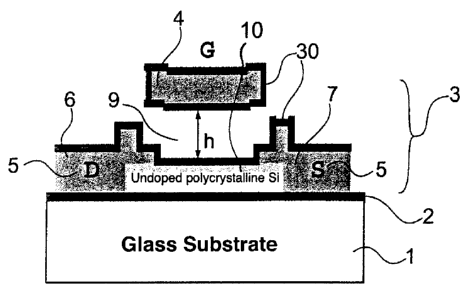
In this first embodiment, the sensor according to
the invention includes a typical field-effect
transistor structure 3, deposited on a glass substrate
covered with a silicon nitride film 2.
The field-effect transistor structure 3 includes a
suspended bridge 4 serving as a gate (G), made of
highly doped polycrystalline silicon.
In this example, the field-effect transistor is
actually a thin-film transistor (TFT). The
polycrystalline silicon bridge is produced by using
surface micro-technology techniques. The structure thus
made using the surface micro-technology techniques is,
CA 02572485 2006-12-29
, . , .
17
for example, called a "Suspended Gate Thin-Film
Transistor" (SGTFT).
However, it is clear that the invention relates to
all field-effect transistor structures for which the
electric field is sufficiently strong to influence the
distribution of the electrical charges present in the
environment.
The field-effect transistor structure 3 includes
an unintentionally doped polycrystalline silicon film
(active layer) 10, deposited on the glass substrate 1
covered with the silicon nitride layer 2. Any other
insulating substrate or substrate covered with any
electrical insulation can also be used. The
polycrystalline silicon layer, for example, is
deposited amorphously and is then crystallised. It can
also be deposited directly in the crystallised state.
Any other undoped or lightly doped semiconductor can
also be used.
A second polycrystalline silicon layer 5, which is
this time highly in-situ doped, is then deposited and
etched to form the source (S)7 and drain (D)6 regions.
It can also be deposited amorphously and then
crystallised or deposited directly in the crystallised
state. It can also be post-doped by any doping method.
Any other highly conductive material can also be used.
Optionally, a silicon dioxide/silicon nitride bi-
layer or a silicon nitride layer alone 8 is then
deposited and etched so as to cover the surface between
the source and drain regions. Any type of electrical
insulating layer can also be used.
CA 02572485 2006-12-29
18
A germanium layer (not shown) is then deposited
and used as a sacrificial layer. An Si02 layer or any
other material compatible with the other layers present
in the structure can also be used as a sacrificial
layer. The thickness h of the sacrificial layer
provides the final value for the height of the air gap
9 (the space under the bridge).
It is recalled that the electric field E created
in the air gap is defined as the ratio between the gate
voltage VGS and the height of the air gap. According to
the invention, this electric field created in the air
gap has a value greater than or equal to a specific
threshold value (50,000 V/cm, and preferably 100,000
V/cm, or even 200,000 V/cm) . The height h of the air
gap and the gate voltage VGs are selected so that this
condition involving the electric field E is met.
This air gap height h is low, for a given gate
voltage VGs, so that the electric field created in the
air gap is strong and thus so that the field effect
will be the predominant effect on sensitivity. In other
words, this height h must be sufficiently low so that a
gate voltage VGs applied to the bridge creates a
sufficiently strong electric field E to influence the
distribution of electrical charges contained in the
environment and present in the air gap. According to
the invention, this height is less than or equal to
1 pm, and preferably less than or equal to 0.5 pm.
Thus, for an air gap height h equal to 0.5 pm, the
electric field E is equal to at least 50,000 V/cm,
100,000 V/cm or 200,000 V/cm, depending on whether the
CA 02572485 2006-12-29
19
gate voltage VGS is equal to at least 2.5 V, 5 V or 10
V, respectively.
A highly in-situ doped polycrystalline silicon
layer 4 is then deposited and etched in order to form
the bridge that serves as a gate (G). Any other highly
conductive material can also be used, which is
compatible with the other layers present in the
structure, and which has sufficient mechanical strength
properties for maintaining the bridge.
A metallic layer (not shown) can then be deposited
and etched to form the electrical source, drain and
bridge (serving as a gate) contacts. The field-effect
transistor structure 3 can also be produced without
this metallic layer.
The sacrificial layer is etched (i.e., eliminated)
so as to free the space (air gap) 9 situated beneath
the bridge 4, either before or after depositing the
metallic contacts, depending on the compatibility
between the various materials used. In this way, the
gaseous environment can occupy this space 9.
The first embodiment of the sensor according to
the invention, which was described above, is sensitive
to various gases. Sensitivity to various environments
has been shown. The structure is not sensitive to
electrically neutral environments. The transistor
characteristic is similar under vacuum, in an 02
environment, or in an N2 environment, for example. In
all of these environments, the threshold voltage is
very high. This high threshold voltage value is normal
considering the usual MOS theory equations wherein the
dielectric constant is 1 and the gate insulator has a
CA 02572485 2006-12-29
thickness greater than or equal to 0.5 Pm. The
transistor characteristic varies in electrically
charged environments.
A theoretical explanation will now be given for
5 the effect characteristic of the invention (new
distribution of the charges in the air gap, owing to
the application of a strong electric field), as well as
for its possible combination with the adsorption effect.
The context here involves the case of a sensor of
10 the invention in which the shift in the threshold
voltage of the transistor is due to:
- the field effect (effect characteristic of this
invention) : a strong electric field is created in the
air gap region, which causes a new distribution of the
15 charges in the air gap; and
- the adsorption effect (well-known effect) at the
surface of a sensitive layer deposited on the active
layer of the transistor. However, as already indicated
above, it is clear that the invention also applies in
20 the case where only the field effect is used (without
being combined with the adsorption effect).
In this case, the threshold voltage VTH of the
sensor (i.e., the value of the gate voltage VGs for
which the drain-source current IDS saturates), is
written as:
VTx - (DMs+2cPF+ QSC _ 1 ejxp(x)dx (1)
C Ceox o
where (DMS is the difference between the work
functions of the gate and the semiconductor, cpF is the
position of the Fermi level in relation to the middle
CA 02572485 2006-12-29
21
of the forbidden band, Qsc is the space charge in the
semiconductor, C is the total capacity per surface unit
between the bridge and the semiconductor, eo,ç is the
total thickness of the insulator (sum of the air gap
height h and the thickness of the insulating layer 8,
e.g., a silicon dioxide (Si02)/silicon nitride (Si3N4)
bi-layer or a silicon nitride (Si3N4) alone), and p(x)
is the charge in the insulator at a distance x from the
bridge.
Any variation of the environment in the air gap
causes a variation in the total charge in the insulator
and a possible variation in its distribution.
Furthermore, chemical reactions on the internal surface
of the air gap (adsorption phenomenon) may occur,
thereby leading to a variation in the parameter (DMs.
In the case of prior techniques, only this latter
variation associated with the adsorption phenomenon is
considered.
However, as this invention proposes, when a strong
electric field is present in the air gap, the
distribution of the charge in the air gap varies, which
causes a variation in p(x). Furthermore, this strong
field can influence the adsorption by pushing the
charges onto the surface of the sensitive layer.
A11 of these effects lead to a variation in (DMs
but also to the last term of the above expression (1).
Consequently, the variation in the threshold voltage
VTH can be very large if, according to the invention,
the effects of a strong electric field are taken into
account.
CA 02572485 2006-12-29
22
Several examples of use of this first embodiment
of the sensor according to the invention will now be
presented in relation to figures 2a to 2h. In these
examples of use, the transistor is a thin-film
transistor with an N-type polycrystalline silicon
suspended gate. The air gap has a height of 0.5 pm. It
is clear that numerous other uses can be anticipated
without exceeding the scope of this invention.
Figures 2a and 2b show that in an NH3 environment
(Fig. 2a) or in an NOz environment (Fig. 2b), the
structure has a significant degree of sensitivity. NO2
and NH3 were selected as test gases for their opposite
effects on the characteristics of the transistors.
Figure 2a shows that when NH3 is introduced, the curve
IDS(VGS) shifts towards the weakest voltages (negative
shift in the threshold voltage). Figure 2b shows that
the introduction of NOz has the opposite effect. Thus,
a shift in the threshold voltage of 6 V is obtained
with 100 ppm of NH3 gas or 2 ppm of NO2.
It is also seen in figures 2a and 2b that, with
this sensor example according to the invention, the
gate voltage VGs must be greater than 10 V in order for
detection to be possible, and thus the electric field
must be greater than 200,000 V/cm (=10V/0.5pm).
Figures 2c and 2d shown that, when smoke is
introduced, the threshold voltage and the slope below
the threshold drop sharply, and the transfer
characteristic saturates. This is particularly visible
on the linear plot of figure 2e.
In the same way, figures 2f and 2g show that, when
humidity is introduced, the threshold voltage and the
CA 02572485 2006-12-29
23
slope below the threshold drop sharply, and the
transfer characteristic saturates. Thus, the threshold
voltage varies by more than 18 V when the humidity
ratio shifts from 25 to 70%.
Figure 2h shows that the sensitivity of the
structure is selective for smoke for low relative
humidity ratios (e.g. when the humidity ratio is held
constant and is lower than 25%).
A second particular embodiment of a sensor
according to the invention, which is suitable for use
in a liquid environment, will no be presented in
relation to figure 3.
This structure differs from that of figure la
(first embodiment suitable for use in a gaseous
environment) in that a silicon nitride layer 30 is
deposited at its surface (and thus in particular at the
surface of the drain 6 and source 5 regions, the active
layer 10 and the suspended bridge 4) . The structure
thus modified can be dipped into a liquid and enable
in-situ measurement in the liquid. Any other material
making it possible to insulate the structure from the
solution can also be used. Furthermore, the contact
regions are covered with resin or any other electrical
insulator.
This structure, for example, is used to measure
the quantity of charges contained in a liquid. It is
called, for example, an "Ion-Sensitive Thin-Film
Transistor" (ISTFT).
Figure 4a shows that a pH sensitivity of 285 mV/pH
is obtained with an air gap having a height equal to
0.5 }im. With an air gap height such as this, the
CA 02572485 2006-12-29
24
variation in the gate voltage, between approximately
6.5V and 9V, corresponds to a variation in the electric
field (in the air gap), between approximately 130,000
V/cm and 180,000 V/cm. Figure 4b shows that this
sensitivity drops to 90 mV/pH for an air gap having a
height equal to 0.8 pm. With an air gap height such as
this, the variation in the gate voltage, between
approximately 6.25V and 7.25V, corresponds to a
variation in the electric field (in the air gap),
between approximately 62,500 V/cm and 72,500 V/cm. This
reduction in sensitivity, in comparison with the case
of figure 4a, shows that the field effect is
predominant in obtaining high sensitivity. In other
words, in a liquid, the modified structure of the
invention provides high pH sensitivity, approximately 2
to 6 times stronger that that of the ordinary ISFET
structures, this sensitivity being dependent on the
thickness of the air gap.
In general, and as explained above in relation to
the formula (1), the high sensitivity to electrically
charged environments of the sensor according to the
invention is explained by the strong field effect that
is created (i.e., the creation of a strong electric
field in the air gap, greater than or equal to 50,000
V/cm, or even 200,000 V/cm) owing, in particular, to a
an air gap having a small thickness h (e.g., h<lpm if
VGS>10V, or h<0.5pm if VGS>5V, in order to obtain an
electric field E greater than or equal to 100,000 V/cm).
When the thickness of the air gap is large and the
electric field E in the air gap is less than 50,000
V/cm (the case of the prior techniques where E is much
CA 02572485 2006-12-29
less than 1,000 V/cm), the field effect is not
sufficient and the distribution of the electric charges
is uniform inside the air gap. This distribution is no
longer uniform when the electric field E becomes strong
5 (greater than or equal to 50,000 V/cm), due in
particular to the fact that the thickness of the air
gap decreases (the case of the technique according to
the invention). The sensitivity of the sensor according
to the invention is heightened because of the larger
10 accumulation of charges on one of the faces of the air
gap (unlike the case of the prior technique where the
distribution of charges is uniform). This accumulation
becomes increasingly larger when the gate-source
voltage and thus the field effect increase. The
15 saturation of the transfer characteristic is explained
by the saturation of the air gap surface when the
electrical charges accumulate as a result of the field
effect. This saturation appears for lower gate-source
voltages (weaker field effect) when the quantity of
20 charges contained in the environment increases. Finally,
the strength of the field effect is clearly
demonstrated because the pH sensitivity decreases when
the thickness of the air gap increases (see above
discussion of figures 4a and 4b).
25 The field effect characteristic of the invention
(new distribution of the electric charges in the air
gap owing to the application of a strong electric
field), as well as its possible combination with the
adsorption effect, will now be illustrated by way of an
example and in relation to figure 5.
CA 02572485 2006-12-29
26
Saline solutions of KC1 and NaCl and a basic
solution of KOH were prepared with exactly the same
concentration.
The pH does not change when saline solutions such
as KCl and NaCl are used. Consequently, when tracking
the transfer characteristics of a sensor according to
the invention, which is placed in these solutions, only
the effect of the electric field on the distribution of
the charges is observed.
On the other hand, in the presence of KOH, the pH
changes and, as a result, not only is the effect of the
new distribution of charges (under the effect of the
electric field) observed, but also the adsorption
effect.
Figure 5 shows the transfer characteristics
(drain-source current IDS - gate voltage VGS) of the
same particular embodiment of a sensor according to the
invention, obtained after the sensor was dipped into
the following liquid environments: deionised water ("DI
Water") and solutions of KOH, KCl and NaCl with the
same concentration.
In the presence of KC1 or NaCl with the same
concentration, the same shift in the transfer
characteristic is observed, in relation to the transfer
characteristic obtained with the deionised water. This
shift is due only to the new distribution of the
electrical charges in the air gap, which results from
the application of a strong electric field. The shift
in the threshold voltage VTH is induced by the
variation in the last term of the above equation (1).
The same distribution of the charges yields the same
CA 02572485 2006-12-29
27
shift. With the KOH solution having the same
concentration, an additional shift is observed. It is
due to the pH of KOH and thus to the charges that are
adsorbed at the surface of the insulating layer
(referenced as 30 in figure 3) consisting of silicon
nitride Si3N4 (first term of the above equation (1) ).
It shall be noted that, in this example, the insulating
layer also serves as a sensitive layer for the
adsorption process. Consequently, in the presence of
KOH, the shift in the transfer characteristic is due,
on the one hand, to the new distribution of charges
(under the effect of the electric field) and, on the
other hand, to the adsorbed charge. Thus, the two
effects combine and contribute to the good pH
sensitivity of this example of a sensor according to
the invention.
Although the invention has been described above in
relation to a limited number of embodiments, those
skilled in the art, upon reading this description, will
understand that other embodiments can be imagined
without exceeding the scope of this invention.
Consequently, the scope of the invention is limited
only by the appended claims.