Note: Descriptions are shown in the official language in which they were submitted.
CA 02572499 2007-O1-18
METHOD FOR ELECTROCHEMICAL FABRICATION INCLUDING USE OF
MULTIPLE STRUCTURAL AND/OR SACRIFICIAL MATERIALS
Background ofthe Tnvention
The invention relates to fom~ing structures by electrochemical deposition.
Microfabrication processes (also referred to as micromachining) ate being
developed and refined for eventual application to the manufacture of complex
devices including machines and instrumentation. These~processes are being
directed to the production of machines of miniaturized devices having
feattffes in
the range of a few microns and in some cases submicron, some of which
currently
exist on a macroscopic scale.
Microfabrication processes include: bulk micromachining, in which
~5 material is removed from regions of a substrate; surface micromachining, in
which
a thin confononal structural layer and one or more sacrificial layers are
deposited
onto a substrate; and LIGA;'~'which generates 2.5-D ex~n~ded shapes by molding
materials around metals elertiodeposited within openings in thick synchmtron-
pmcessed photoresists. These processes are used to produce'structures of
simple
. geometries (e.g., they can be defined by 1-4 different cross sections), and
are
usually customized for each application.
Solid freeform fabrication, which is also referred to as rapid prototyping, is
used to manufacture macroscopic parts from hundreds of layers by generating
one
layer at a time. These processes produce features typically greater than 50-
I00 ~m
in width using layers, typically greater than SO-150 l.im thick. These process
typically generate a layer serially. These processes employ structures for
supporting the part being manufactured. The support structures are often
customized to the part.
la
CA 02572499 2007-O1-18
In one aspect, the invention features an electroplating method that includes:
a)
contacting a first substrate with a first article, which includes a substrate
and a
conformable mask disposed in a pattern on the substrate; b) electroplating a
first
metal from a source of metal ions onto the first substrate in a first pattern,
the first
pattern corresponding to the complement of the conformable mask pattern; and
c)
removing the first article from the first substrate.
In preferred embodiments, the method further includes electroplating a second
metal from a second metal ion source onto the first substrate. In one
embodiment, the
step of electroplating the second metal includes: a) contacting the first
substrate with
a second article including a substrate and a conformable mask disposed in a
pattern
on the substrate; b) electroplating a second metal onto the first substrate in
a second
pattern, the second pattern corresponding to the complement of the conformable
mask
pattern of the second article; and c) removing the second article from the
first
substrate. The method can further include building additional layers.
In one embodiment, the invention features an electroplating method that
includes repeatedly contacting a substrate with a patterned conformable mask;
electroplating a first metal form a source of ions onto the substrate in a
pattern, the
2o pattern corresponding to the complement of the conformable mask pattern;
and
removing the mask from the substrate.
In another embodiment, the invention features a method for manufacturing an
element that includes forming a mufti-layer structure by repeatedly forming
layers
according to the above-described electroplating methods.
In another aspect, the invention features an electroplating article that
includes
a substrate having a first major surface and a conformable mask disposed in a
pattern
on the first major surface of the substrate. The article is capable of
electroplating a
pattern of metal complementary to the pattern of the conformable mask onto an
electrode when the article is placed in contact with the electrode in the
presence of a
3o metal ion source and subjected to an electric field.
2
CA 02572499 2007-O1-18
In other aspects, the invention features an electroplating apparatus that
includes an electrolyte, which includes ions of a first metal and ions of a
second
metal, an anode in contact with the electrolyte, a cathode in contact with the
electrolyte, and a first article (e.g., the above described electroplating
article) in
contact with the electrolyte.
In one embodiment, the electroplating apparatus includes a first
electroplating
reservoir that includes an electrolyte, which includes a first metal ion,
disposed within
the first reservoir, an anode in contact with the electrolyte, a cathode in
contact with
the electrolyte, and an article (e.g., an article described above) in contact
with the
t o electrolyte; a second electroplating reservoir that includes an
electrolyte, which
includes ions of a second meal, disposed within the second reservoir, and an
anode in
contact with the electrolyte.
In another aspect, the invention fa method for manufacturing an
electroplating article. The method includes: a) applying a conformable mask to
an
is article comprising a first substrate and a patterned resist disposed on the
fast
substrate; b) contacting a second substrate to said conformable mask such that
the
conformable mask obtains a pattern complementary to the resist pattern; c)
separating
the first substrate from the conformable mask (the conformable mask remaining
adhered to the article); and d) removing the resist.
2o In one embodiment, the method for manufacturing an electroplating article
includes providing a porous medium having a first surface; b) treating said
porous
medium to create one or more nonpomus regions; c) applying a film to said
first
surface of said porous medium; d) patterning the film to create a patterned
mask; and
e) removing at least a portion of the one or more nonporous regions.
25 In other aspects, the present invention is directed to the calculation,
storage
and retrieval of cross section geometry of a three dimensional object for
generation
of patterned masks reflecting that geometry and for use in an electroplating
method. The data and control processes of the invention can be implemented by
a
software application prograr executed in a general purpose computing system.
3o The data and control processes of the invention can be embodied in an
electroplating method implemented via the application prograr and also in an
CA 02572499 2007-O1-18
article of manufacture, in the form of a data storage medium, that stores
application
program code arranged to carry out that method upon execution by a processor.
The electroplating methods and articles allow fabrication of devices from thin
layers of materials such as, e.g., metals, polymers, ceramics, and
semiconductor
s materials. The electroplating methods produce relatively homogeneous,
isotropic
elements (e.g., devices) without interlayer junctions. The electroplating
methods can
be performed at low temperatures, thus allowing substrates such as integrated
circuits
and silicon wafers to be used as plating substrates.
The electroplating methods of the invention can be used to fabricate devices
of freeform geometry including high aspect ratio devices, hollow devices with
internal features, devices with cantilevered and "chandelier" geometries, and
functional assemblies of interconnected, stationary or moving parts (i.e.,
devices
fabricated in an assembled state). The electroplating articles, apparatus, and
methods
also are particularly useful in mass production of devices.
i5 Other features and advantages of the invention will be apparent from the
following description of the preferred embodiments thereof, and from the
claims.
Fig. 1 is view taken in cross section of an electroplating article according
to
2o one embodiment of the invention;
Fig. 2 is a view taken in cross section of an electroplating article according
to a second embodiment of the invention;
Fig. 3 is a diagram of a first embodiment of a method for forming an
electroplating article;
25 Fig. 4 is a diagram of a second embodiment of a method for forming an
electroplating article;
Fig. 5 is a diagram of a third embodiment of a method for forming an
electroplating article;
Fig. 6 is a diagram of a fourth embodiment of a method for forming as
3o electroplating article;
4
CA 02572499 2007-O1-18
Fig. 7 is a diagram of a fifth embodiment of a method for forming an
electroplating article;
Fig. 8 is a diagram of a sixth embodiment of a method for forming an
el~troplating article;
Fig. 9 is a diagram of a seventh embodiment of a method for forming an
electroplating article;
Fig. 10 is a diagram of a method for forming a deposit according to an
electroplating method of the invention;
Fig. 11 is a diagram of a method according to a first embodiment of the
to electroplating method of the invention;
Fig. 12 is a diagram of a method according to a second embodiment of the
electroplating method of the invention;
Fig. 13 is a diagram of a method for fabricating an element on an integrated
circuit;
15 Fig. 14 is a diagram of a method for assembling elements fabricated
together;
Fig. 15 is a diagram of an element manufactured according to one
embodiment of the el~troplating method of the invention;
Figs. I6a d are views taken in cross section of elements manufactured
20 according to one embodiment of the invention;
Fig, 17 is an electroplating apparatus according to one embodiment of the
present invention;
Fig. I 8 is a view taken in cross section of a substrate in contact with an
electroplating article;
25 Fig. 19 is a top view of a portion of as electroplating apparatus of the
invention;
Fig. 20 is a top view of a portion of an electroplating apparatus according to
a third embodiment of the electroplating apparatus of present invention;
Fig. 21 is a top view of a portion of an electroplating apparatus according to
3o a fourth embodiment of the electroplating apparatus of the present
invention;
CA 02572499 2007-O1-18
Fig. 22 is a view taken in cross section of one embodiment of an
electroplating article holder of the present invention;
Fig. 23 is a view taken in cross section of a second embodiment of an
electroplating apparatus of the present invention;
Fig. 24 is a highly enlarged view taken in cross section of a substrate in
position in the electroplating apparatus of Fig. 23;
Fig. 25 is a view taken in cross section of a third embodiment of a portion
of an electroplating apparatus of the invention;
Fig. 26 is a view taken in cross section of another portion of the
Io electroplating apparatus ofFig. 25;
Fig. 27 is a diagram of a three dimensional object (shown in two
dimensions) with cross section lines indicated;
Fig. 28 is a functional block diagram of a computing system configured for
calculation of cross sections of a three dimensional structure and for driving
an
electroplating apparatus of the present invention;
Fig. 29 is a flow diagram illustrating a method for generating mask pattern
files and apparatus control files;
Fig. 30 is a flow diagram illustrating a method for manufacturing a three
dimensional object;
2o Fig. 31 is a view taken in cross section of an electromagnetic motor;
Fig. 32 is a diagram of an electroplating method employing more than one
article according to a third embodiment of the electroplating article of the
invention.
The invention features electroplating methods, apparatus and articles that
enable the
manufacture of elements having complex structures. The electroplating methods
include selective electroplating of layers that may include both stnzctural
materials
{e.g., metals) and support (i.e., sacrificial) materials; and subsequent
removal (e.g., by
3o etching, melting, or electrolytically dissolving) of the support materials.
The
structural material remaining after removal of the support material defines an
element
6
CA 02572499 2007-O1-18
such as a microscopic or mesoscopic device. The electroplating methods employ
electroplating articles that include a patterned conformable mask, optionally
adhered
to a support such as an electrode or a porous medium.
In general, the invention features electroplating articles for use in
electroplating methods. The electroplating method occurs in an electroplating
apparatus that includes an electmpiating bath filled with electrolyte, an
anode, and
a cathode. The electrolyte contains metal ions and, optionally, other
additives. The
anode can be part of the electroplating article, as describai below, or can be
located at a distance from the article. Throughout this application, the
substrate to
o be plated functions as the cathode unless otherwise specified. To simplify
the
description, the materials are referred to as metals and similar features are
indicated with the same reference numerals.
CA 02572499 2007-O1-18
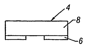
Referring to Fig. 1, electroplating articles 4, of the invention include a
patterned conformable mask 6 adhered to a support 8. The electroplating
article
can also be a patterned conformable mask. The support can be a porous medium
(e.g., a filter), an anode, and combinations thereof. The article can include
a
plurality of different mask patterns on a single support'. The different mask
patterns can be contacted by a substrate in a predetermined sequence to
sequentially plate a plurality of metal layers where each metal layer has a
pattern
corresponding to the complement of the mask pattern contacted, to form a multi-
layered element. Referring to Fig. 2, electroplating article 4 can include one
or
1 o more edge masks on the outer surface of the article, for confining the
metal being
plated.
Contact between the electroplating article and the substrate to be plated is
made by pressing the patterned mask against the substrate using a well-
controlled,
uniform pressure. The appropriate masking pressure will prevent flash (i.e.,
the
1 S deposition of metal in the area covered by the mask), and will prevent
distortion of
the features defined by the mask. When the electroplating article is removed
from
contact with the substrate, the mask remains adhered to the electroplating
article.
A variety of methods can be used to improve release of the mask from the
substrate to be plated so as to,prevent delamination of the mask from the
support; .
2o . gradually peeling the electroplating article (if flexible) off of the
substrate with the
aid of a dull blade; adding a non-stick/lubricating compound to the
electrolyte;
coating the mask surface with a non-stick composition (e.g., sputtered
polytetrafluoroethylene); and vibration (e.g., ultrasound).
25 The patterned. conformable mask is sufficiently deformable (e.g.,
elastically
deformable) to permit conformance of the mask to the surface of a substrate to
be
plated to maximize contact between the mask and the substrate, and to minimize
(preferably eliminate) the presence of gaps between the mask and: the
substrate.
Maximizing contact between the mask and the substrate minimizes the potential
3o for flash formation. The mask is also sufficiently durable to enable
repeated use
(i.e., contacting with and removing from a substrate). The mask is
sufficiently
CA 02572499 2007-O1-18
rigid and thin to prevent distortion of the mask features (i.e., the positive
and
negative features constituting the closed and open features of the mask
pattern
respectively) by the masking pressure. The mask preferably is relatively thick
compared to its peak and valley roughness and the curvature of the substrate
to be
plated.
The mask preferably exhibits very high volume electrical resistivity (e.g.,
10-~4 Ohm=cnp), has a very low permeability to ions in the electrolyte
solution, and
is chemically non-reactive with the plating electrolytes at the temperatures
at
which the plating operation is conducted. The mask can be hydrophilic or
t o hydrophobic, with hydrophilic being preferred. In the case of hydrophobic
materials, relatively higher amounts of wetting agents can be included in the
electrolyte to ensure wetting of the mask material.
The mask preferably is capable of forming a strong bond (e.g., a chemical
or mechanical bond) to the support, such that small (e.g., 15x15 pm) isolated
positive features are not delaminated by the mask fabrication process, normal
handling of the mask or by removal of the mask material from the substrate to
be
plated.
The patterned mask is preferably substantially planar and smooth to enable
conformance to the substrate to be plated. The mask is capable of being
patterned
with negative and positive features of.varying dimensions (e.g., 10-25 N.m or
smaller, such as submicron), preferably with no mask residue blocking the
negative
features of the mask pattern. The pattern of the mask includes apertures
(i.e.,
negative features) extending through the mask thickness and defined by one or
more side walls of the mask. The mask features preferably have a substantially
planar wall profile and may have a slight wall angle (e.g., slightly divergent
toward
the substrate to be plated) re-contacting the mask to the substrate in the
presence of
an existing deposit.
The mask can be compound so as to include one or more layers of material,
e.g., a relatively rigid layer (i.e., a high aspect ratio photoresist, e.g.,
SU-8
9
CA 02572499 2007-O1-18
commercially available from MicroChem Corporation and synchrotron processed
polymethylinethacrylate), and a conformable layer. Another example of a useful
rigid layer is a positive photoresist such as Clariant AZ4620, which can be
patterned by exposing it to ultraviolet light through the patterned
conformable
layer.
Examples of useful masking compositions include elastomers such as, e.g.,
polydimethylsiloxane (i.e., silicone rubber) commercially available, e.g.,
under the
trade designation Sylgard from Dow-Coming (e.g., Sylgard 182, and 184), and
under the trade designation RMS-033 from Gelest. The maslting compositions can
include other additives, e.g., photoinitiators, fillers, arid hydrogen
getters.
The porous medium has interconnected pores and is permeable to ions and
additives present in electrolyte compositions. The porous medium can have one
or
more layers of varying porosity. The porous medium preferably has a pore size
considerably finer than the minimum negative feature of the mask. The pores
are
preferably uniform in open area, e.g., the open area of any 20 pro square of
the
medium is consistent to 1 %. Particularly useful porous mediums, when used as
filters, have a particle retention rating of 0.3-3Eim. For those porous
mediums that
include multiple porous layers, each porous layer can vary in porosity and
pore
2o size, with the porous medium in closest proximity to the substrate to be
plated
exhibiting the above characteristics. The surfaces of the porous medium that
contact the mask should be sufficiently flat and smooth to ensure that the
surface
of the adhered mask that contacts the substrate to be plated is also flat and
smooth.
The porous medium is chemically non-reactive with the electrolyte solution
at the operating temperature of the electrolyte bath. Preferred porous mediums
are
hydrophilic. The porous medium preferably is permeable to gas to allow venting
of gas bubbles generated during the electroplating method.
Preferably the porous medium is free from shedding (i.e., does not release
portions of itself into surrounding fluid), and is sufficiently durable so as
to
3o v~rithstand multiple electroplating operations. Examples of suitable porous
medium
CA 02572499 2007-O1-18
materials include rigid, hydrophilic, slip cast cermnic disk porous mediums
(commercially available from Coors Ceramics) and hydraphiiized membrane
porous mediums made from, e.g., polypropylene (commercially available under
the
trade designation GH from Gelman), polyvinylidenefluoride (commercially
available under the trade designation Durapore from Millipore) and
polytetrafluoroethylene (commercially available under the trade designation
LCR
from Millipore). Rigid porous mediums can provide masking pressure when
supported by their edges alone.
Particularly useful highly permeable, porous mediums include relatively
thin, flexible, porous membranes. Porous membranes can be combined with a
more rigid porous m~ium, which serves as a backing to provide the requisite
pressure for masking applications. The porous membrane can be sandwiched
between the more rigid porous medium and the mask and the porous medium can
be used to supply the requisite masking pressure for the plating operation.
The
t 5 more rigid porous medium can have a relatively more coarse (i.e., larger)
porosity
than that useful for direct contact with the mask. Porous membranes can be
integrated with the mask composition (or transformed into a mask).
To assist handling, porous membranes can be installed in the drumhead
fixture described below, or temporarily adhered to a rigid fiat substrate
(e.g., a
2o silicone wafer, glass) with an adhesive composition (e.g., dry film
photoresist).
Porous membranes can be processed while adhered to the substrate and, after
processing, removed by dissolving the adhesive.
Masking pressure can be applied to the porous membrane by the
momentum of a stream or jet of electrolyte impinging on the membrane from
25 behind, optionally in combination with dense particles incorporated into
the
electrolyte, and increasing the viscosity of the electrolyte, for example, by
the
addition of a polymer. Masking pressure can also be applied to the membrane by
sealing the membrane against the wails of the tank of the electroplating
system and
then pressurizing the electrolyte, causing the membrane to be pushed against
the
30 substrate to be plated. A dummy substrate can be used when the substrate to
be
plated is smaller than the porous medium to prevent the membrane from bulging.
11
CA 02572499 2007-O1-18
One example of an electroplating method that employs a porous membrane
includes pressing a relatively more rigid porous medium against the mennbrane,
applying current, depositing a metal for a period, removing the current,
withdrawing the rigid porous medium from contact with the membrane, slightly
displacing the relatively more rigid porous medium in its own plane (e.g., in
an
orbital or linear fashion), and repeating the cycle. Displacing the relatively
more
rigid porous medium during each cycle allows a different portion of the rigid
porous medium to make contact with the membrane. Preferably the
masklmembrane separates from the substrate to be plated while the relatively
more
1o rigid porous medium is separated from the membrane so as to allow exchange
of
fluids between the microvolume and bulk electrolyte.
Another membrane plating method includes pressing a granular medium,
tiny spheres, or rollers against the membrane using, e.g., a rigid scre,~en.
The tiny
spheres and rollers can be rotated in a pattern (e.g., a linear pattern using
linear
movement or a circular pattern using an orbital movement) on the membrane
continuously or intermittently so as to average the local non-uniformities in
pore
structure of the rollers/spheres. Preferably the amplitude of movement is
equal to
(more preferably several times greater than) the diameter of the sphere or
cylinder.
Preferably the spheres/cylinders are relatively small and the membrane is
relatively
2o thick. The sphereslcylinders can be made of the metal being plated.
The electroplating article can consist of a patterned mask on an anode. The
anode can be soluble ar insoluble, rigid or flexible, porous or nonporous, and
can
include an erodable layer (e.g., a metal layer) supported by a conductive
material
that does not erode (e.g., platinized titanium). The anode can be of any
dimension
including a thin flexible sheet of metal.
A soluble anode will tend to erode during use. The anode can be
"redressed" periodically by reversing the polarity of the anode and plating
metal
back onto the anode through the negative features of the mask. The excess
metal is
3o supplied by the electrolyte in conjunction with another anode according to,
e.g.,
through-mask plating processes used in electronics manufacturing. For a system
in
12
CA 02572499 2007-O1-18
which the mask is physically supported by and attached to a porous medium, and
an anode is located directly behind the membrane, moving the anode will
prevent
localized erosion of the anode.
Forming Eiectro 1p atin_g Articles
In general, methods for forming electroplating articles include applying a
solid mask or liquid masking composition to a support, i.e., an anode, a
porous
medium and combinations thereof. The solid mask can be pa#erned prior or
subsequent to attachment to the support. Liquid masking compositions can be
1o patterned'on a non-porous substrate (e.g., inert material, or a material
that can be
dissolved or melted (e.g., substrates of plastic, lacquer, or low melting
point
alloy)), cured (i.e., crosslinked, polymerized, hardened, solidified, gelled,
and
combinations thereofj, and attached to a support or patterned and solidified
directly
on the support.
Pr~aration of the Support
It is preferable to planarize the surface of the support that will receive the
mask, so as to provide a smooth flat surface for receiving the mask. When
applying
the mask to an anode, it is preferable to first prepare the anode surface so
as to
maximize adhesion to the mask. Examples of useful anode surface preparation
2o methods include chemical microetching, lapping, sandblasting, and sintering
a thin
layer.of powder onto the surface. A chemical adhesion promoter (e.g., Sylgard
"~'
Prime Coat) can also be used.
A variety of methods can be used to maintain or improve adhesion of the
mask to a porous medium. These methods include meltiTig the mask while
pressing
it into the porous medium resulting in a mechanical interlocking of the mask
with
the porosity of the porous medium, and applying an adhesive.composition
between
the mask and the porous medium. Adhesion of the mask to the porous medium can
also be enhanced by employing an adhesive that is a meltable material (e.g.,
glass),
which can be dry deposited (e.g., sputtered) onto the surface of the patterned
mask.
3o When using an adhesive composition, it is preferable to employ methods that
13
CA 02572499 2007-O1-18
confine the adhesive composition to the areas located between the mask and the
support (i.e., preventing the adhesive from bridging a negative feature that
is only a
few microns wide).
Liquid masking composition has a tendency to soak into (i.e.,
uncontrollably absorb into) the pores of a porous medium. A variety of methods
can be employed to reduce "soak in" in regions of the porous medium that are
to
remain porous. Examples of suitable methods for preventing soak in include:
supplying pressurized air to one side of the porous medium; treating the
porous
medium with a temporary filler composition that soaks in and fills the pores
and
1o then solidifies to form a barrier to penetration of the liquid masking
composition;
and treating the porous medium with a temporary filler composition that is
immiscible with and denser than the liquid masking composition. The surface of
the porous medium can be abraded after infiltrating the pores with filler
composition to expose uncoated and unfilled surfaces allowing direct adhesion
of
15 the mask to the support. The filler composition can be dissolved or
otherwise
removed from the porous medium after the liquid masking composition has been
cured to a solid.
Examples of useful filler compositions include acetone-soluble waxes and
lacquers, soluble waxes used for investment casting cores, water soluble
salts, gels,
2o Crystal Bond 509, soluble thermoplastics, and phase-change materials (e.g.,
ice,
electrorheological fluids).
Referring to Fig. 3, one example of a method for rendering a porous
medium temporarily nonporous using a filler composition includes: spinning a
thin
layer of a liquid filler composition 132 onto a relatively flat surface 13I
(e.g., a
25 silicon wafer) (preferably the thickness of the filler composition layer is
adjusted
so as to fill the pores of the porous medium to a predetermined height);
contacting
a first surface I36 of porous medium 130 to the spun on filler composition 132
(Fig. 3a), allowing filler composition 132 to seep into the pores of the
porous
medium to a predetermined depth (Fig. 3b); solidifying the filler composition
132;
3o and applying (e.g., by spinning on) a sufficient amount of fiquid masking
composition 134 to a second surface 138 of the porous medium I30 opposite the
14
CA 02572499 2007-O1-18
first surface through which filler composition 132 entered the porous medium
130.
Liquid masking composition 134 is applied so as to produce a layer of masking
composition of desired thickness on the surface of the porous medium. The
remainder of the masking composition 134 can seep into the porous medium (for
purposes of adhesion) only to the surface of the solidified filler 132. The
method
fiuther includes curing the masking composition 134; removing solidified
filler
132; etching the negative features of the mask through the layer of porous
medium
130 that is saturated with masking composition 134 to at least a depth at
which the
solidified filler 132 existed (Fig. 3d).
1o Other methods for preventing or limiting soak in include restricting the
volume of liquid masking composition that is applied to the porous medium to
only
a fraction of the pore volume in the porous medium causing the liquid to only
partially fill the pores. One such method includes spraying a liquid masking
composition onto the porous medium, while carefully controlling the flow rate
and
speed of the spray pattern. Another method involves spin coating the liquid
masking composition onto a non-absorbing sheet to obtain a uniform thin layer,
and placing the porous medium in contact with the spun on liquid masking
composition. When the porous modium is peeled away from the sheet or the sheet
is dissolved or melted, a thin coating of masking composition is transferred
to the
2o porous medium (i.e., the masking composition remains adhered to the porous
medium). The liquid masking composition can be cured prior to or subsequent to
removal of the sheet.
Another method for preventing soak in involves applying the liquid
masking composition to a porous medium while the porous medium is spinning at
high speed; the centrifugal forces spread the masking composition into a thin
layer
before it has had time to soak in excessively.
Another approach to preventing soak in involves forming a barrier layer at
or near the surface of the porous medium. After processing, the barrier layer
(and
optionally, some of the porous medium) is removed from the negative features
of
the mask, so as to expose the porosity of the porous medium. Optionally, to
CA 02572499 2007-O1-18
improve adhesion of the mask to the support, the regions of the barrier layer
that
will correspond to the positive features of the mask can be removed prior to
application of the mask. The barrier layer can be removed using various
techniques
including, e.g., chemical etching, dry etching, ion milling, Laser machining,
and
melting (e.g., for thermoplastic based barriers). The barrier layer can also
be
formed by applying another material to the surface of the porous substrate,
e.g.,
laminating a film of a solid material, such as dry filin photoresist onto the
porous
medium; applying a liquid barrier layer, preferably of high viscosity, using
one of
the techniques discussed above that restrict soak-in volume; coating the
porous
to medium with a thin layer of powder and melting the powder layer so as to
form a
non-porous coating; depositing a barrier film by vacuum evaporation,
sputtering,
CVD, or other process; and combinations thereof.
In the case of a porous anode, soak in can be prevented using a variety of
methods which include, applying a nonporous Layer to the surface of the porous
is anode and, after patterning the mask, removing the nonporous layer in the
negative
areas of the mask to expose the anode; sintering a partly-compacted powder in
a
mold, patterning the mask, and immersing the structure in an etchant that
attacks
the metal of the anode, such that the outer non-porous layer of sintered anode
materiai is dissolved (in the unmasked regions); melting the surface of the
anode
20 (e.g., by flame, or contact with a hot surface); temporarily filling the
surface pores
with a material, e.g., metal electrodeposited onto the porous surface; and by
applying a nonporous barner layer between the mask and the anode.
Patterning a_n_d Fabricating the Electronlati~,g Article
A variety of methods can be used to pattern the electroplating article.
25 Referring to Fig. 4, a method for forming an electroplating article is
shown. The
method includes foaming a micromold 140 by coating (e.g., by spinning) a layer
of
resist 142 (e.g., photoresist commercially available under the trade
designation SU-
8 5 from MicroChem Corp.) onto a substrate 144 (e.g., a silicon wafer).
Preferably
the layer of photoresist has a thickness a few microns greater than that the
desired
3o thickness of the final mask. The photoresist can be patterned using a
photomask
and, in the case of photopattemable resist compositions, a light source (e.g.,
a LTV
16
CA 02572499 2007-O1-18
light source). A positive feature of the resist corresponds to a negative
feature of
the mask. Optionally, the micromold can be made from a non-stick material such
as, e.g., polytetrafluoroethylene or polypropylene, and can include a pattern
formed, e.g., by reactive ion etching or excimer ablation, or micromolded from
a
master mold according to processes similar to processes used in the
fabrication of
compact discs.
The micromold surface including the photoresist and the substrate can be
passivated by allowing the micromold to be exposed to vapors of, e.g.,
(tridecaffuoro-1,I,2,2-tetrahydrooctyl)-1-trichlorosilane (commercially
available
from United Chemical Technologies). A liquid masking composition 146 is then
poured over the raised pattern defined by the patterned photoresist. Support
148 is
then pressed against micromold 140. Uniform pressure is applied such that
liquid
masking composition 148 is forced out of the area 150 located between the
raised
portions (i.e., positive featuxes) of the resist pattern and the surface of
support 148.
Preferably, liquid masking composition 146 is completely squeezed out of the
areas 150 corresponding to the positive features of resist 142. The entire
assembly
152 remains in this mating relationship until the liquid masking composition
has
cured. For a heat-curable masking composition, the assembly can be transferred
to
an oven to cure.
2o After cure, excess mask material 154 surrounding support 148 is removed.
In the case of a mask that has been cured in the oven, the assembly is quickly
disassembled to minimize differential thermal contraction between support and
the
mold. The support and cured mask 156 is pulled away from mold 140 such that
cured mask 156 detaches from micromold 140, yet remains adhered to support
148. Mask i56 exhibits a pattern inverse to that of micromold 140. Micromold
140 can be reused. If necessary, micromold 140 can be cleaned to remove mask
residue. One example of a useful silicone cleaning composition is a silicone
stripper, e.g., Amtex CCR (commercially available from Amtex Chemical Corp.).
Any residual layer of masking composition remaining is negative features
158 of mask 156 can be removed using dry etching (e.g., RIE with a mixture of
02
and CF4 gas), which may also reduce the thickness of the positive features of
the
CA 02572499 2007-O1-18
mask. Uniform etching extending to the edge of the support can be accomplished
by surrounding the support with a "dummy" substrate preferably of similar
composition, such that non-uniformities due to edge effects are out of the
area of
interest.
When the mask is adhered to a porous medium, the etch may be continued
to remove any barrier layer present in the porous medium from the negative
features of the mask and may be continued until a porous portion of the porous
substrate is removed. If pores in a porous medium have been filled or are non-
existent, the pores are re-established or established , e.g., by reactive ion
etching.
1o Another method for forming an electroplating article is shown in Fig. 5.
The method includes patterning a photoresist 142 onto a support 148 {i.e., the
porous medium or the prepared anode) to the approximate thickness desired for
the
final mask. The areas of support 148 occupied by resist 142 correspond to
negative
features of the mask through which metal can be deposited. When patterning a
porous medium that includes a barrier, the porous medium can be etched to
remove
the barrier layer from those areas of the porous medium that are not covered
by
resist. The method further includes applying a liquid masking composition 146
to
support 148, and optionally vacuum degassing the masking composition. A flat,
smooth, non-stick {e.g., PTFE) sheet 160 is then pressed against resist 142,
and
2o liquid masking composition 146 parallel to support 148, and pressure is
applied to
squeeze the liquid masking composition 146 out from between resist 142 and
sheet
160. Masking composition 146 is then cured, sheet 160 is removed, and residual
masking composition overlaying the resist is removed, e.g., by etching {e.g.,
reactive ionization etching using a mixture of 02 and CF4 gas). Resist 142 is
then
removed to expose areas of the support previously occupied by the resist. When
patterning a porous medium, mask material that has seeped into the negative
features of the mask from neighboring positive features can be removed by
etching
both mask and porous medium to the required depth. If pores of the porous
medium have been filled or are non-existent, the pores can be established or
re-
3o established.
I8
CA 02572499 2007-O1-18
Referring to Fig. 6, another method for forming an electroplating article
includes applying (e.g., by spinning on) a layer of photopatternable liquid
masking
composition 146, e.g., RMS-033 (commercially available from Gelest) in
combination with a photoinitiator (e.g., 2,2-dimethoxy-2-phenyl acetophenone
(commercially available from Polysciences, Tnc.)), to support 148. Liquid
masking
composition 146 can be covered with a thin, oxygen-impermeable film (e.g.,
Mylai~'to protect the composition from contact with oxygen. Masking
composition 146 is then exposed to patterned light (e.g., LIV light
transmitted
through a photomask 162) to selectively cure the mask composition. The film is
Io removed and the photopatternable masking composition is developed (e.g., by
dissolving with xylene) removing uncured masking composition 146. If a
nonporous barrier layer exists, it is removed (e.g., by dry etching) from the
negative features of mask 156. Pores are established if necessary. For those
photopatternable masking compositions that are negative working the pomus
i5 medium can be completely saturated with masking composition until there is
a
surface layer of masking composition having the desired thickness. After
photopatteniing, the unexposed masking composition material (including that in
the pores) is dissolved in the developer.
When patterning a porous medium, the porous medium can be tinted a dark
2o shade or coated with an antireflection composition to reduce the amount of
light
scattered from the textured surface.
Referring to Fig. 7, another method for making an electroplating article is
shown. The method includes applying a liquid masking composition 146 (or a
solid mask) to support 148; curing liquid masking composition to form. a
solidified
25 mask 156; coating mask 156 with either a thick resist 164 or a thin resist
disposed
on a thin metal layer (not shown); patterning resist 164 and, in the case of a
metal
layer, using the patterned resist to pattern the metal layer (e.g., by etching
or lift-
of~; removing (e.g., wet etch, dry etch, or ion mill) mask 156 using thick
resist
164 (and metal layer if present) as a mask; and in the case where the
substrate is a
30 porous medium, preferably removing the top layer of the porous medium to
open
19
CA 02572499 2007-O1-18
pores; and removing, e.g., by stripping, the remaining resist 164 (and metal
layer if
used).
Referring to Fig. 8, a method for forming an electroplating article is shown
which includes: applying a liquid masking composition 146 (or a solid mask) to
support 148 to the desired thickness; curing (if liquid) the masking
composition to
form solidified mask 156; exposing solid mask 156 to patterned ultraviolet
light of
intensity and wavelength suitable for ablating the mask and support material,
e.g.,
a LTV excimer laser beam; ablating mask 156 until support 148 is exposed; and,
when patterning a porous medium, ablating barrier layer 170 (if present) and,
if
1o necessary, the top layer of the porous medium to open pores.
Methods similar to methods used in relief printing can also be used to
fabricate electroplating articles. One example of such a method includes:
applying
a liquid masking composition to a relief pattern, which might be produced by
pattenaing a high aspect ratio photoresist such as AZ4620 or SU-8; pressing
the
relief pattern/masking composition structure against a support such that the
masking composition adheres to the support; and removing the relief pattern.
The
formed electroplating article includes a support having a mask patterned with
the
inverse pattern of the relief pattern.
Another example of such a method includes: creating a relief pattern on the
2o support by etching of the support, or applying a durable photoresist, e.g.,
SU-8;
coating a flat, smooth sheet with a thin, uniform layer of liquid masking
composition; stamping the support/resist against the coated sheet (i.e., like
a stamp
and inkpad) to quickly mate and unmate the supportlresist and the masking
composition (preferably the support and the sheet are kept parallel); and
curing the
liquid masking composition.
Referring to Fig. 9, a method for forming an electroplating article is shown
in which a surface layer of porous medium 148 is saturated with a liquid
masking
composition to the thickness of the desired mask. Liquid masking composition
is
solidified producing a matrix 174 of solid mask 156 and porous medium 148.
3o Matrix 174 is then patterned, e.g., by etching or ablating selected areas
of the
matrix to a depth at least equal to the depth of the matrix "layer", to form
CA 02572499 2007-O1-18
electroplating article 176. Alternately, the method can include saturating the
entire
porous medium with liquid masking composition, pattern curing the liquid
masking composition, and removing the uncured masking composition.
Other methods of forming electroplating articles include, e.g., applying
s masking composition selectively to a support by such processes as screen
printing,
stencil printing and inkjet printing; and for porous mcdiums, melting a
surface
layer of the porous medium and forming negative features in the surface of the
porous medium by etchinglablating through the melted layer to expose the pores
of
the pomus medium and generate a relicf pattern. The methods for forming
to electroplating articles.can also include etching the negative features
(i.e., windows)
of the mask pattern to increase the amount of relief on the electroplating
article. In
the case of a porous medium and a printed silicone mask, etching can be
conducted
by an oxygen plasma.
The Electroplalj~~
15 In general, the invention features electroplating methods that include
contacting a substrate to be plated with an electroplating article of the
invention;
selectively electroplating a first metal, e.g., a support or sacrificial
metal; and
electroplating a second metal, e.g., a structural metal. The step of
electroplating a
second metal can include selectively electroplating the second metal using an
2o electroplating article of the present invention or blanket depositing the
second
metal. The electroplating method can be used to plate a single layer of metal
or the
method can be repeated such that additional metal is plated onto previously
plated
metal layers producing a mull-layered structure. After a predetermined number
of
layers) have been plat~i, at least a portion of the support metal can be
removed,
25 e.g., by etching. The structural metal that remains defines a microscopic
or
mesoscopic device.
The method can also employ two el~tropiating articles to plate a single
Layer of one metal. Referring to Fig. 10, a first metal is plated in a first
pattern
230, the same metal is then plated in second pattern 232, to form plated metal
layer
30 234. Second pattern 232 may overlap first pattern 230.
21
CA 02572499 2007-O1-18
One example of an electroplating method of the invention is shown in Fig.
I 1. The method includes contacting a substrate to be plated 2 with first
article 4,
which includes mask 6 and support 8, in the presence of a first metal ion
source
(i.e., electrolyte and anode IO), depositing a first metal 12, e.g., a
sacrificial metal,
contacting substrate 2 with a second article 14, which includes mask 16 and a
support 18, depositing a second metal 20, e.g., a structural metal, in the
presence of
a second metal ion source (i.e., electrolyte and anode 22), optionally
planarizing
the layer, and repeating this method using differently patterned
electroplating
articles 4a, 4b, 14a, 14b to produce mufti-layered structure 24, which, after
etching
aII of sacrificial metal 12, becomes element 26. The second article can
include a
mask that has oversized positive features such that the surface area of one or
more
positive features of the mask extends beyond the corresponding surface area of
the
first plated metal.
The element formed during the electroplating method can remain attached
to the substrate or can be removed from the substrate. One method for removing
the element includes plating a first layer of support material onto the
substrate such
that etching removes the source of attachment of the element to the substrate.
Another electroplating method is depicted in Fig. 12. The electroplating
method includes: contacting a substrate to be plated 2 with an electroplating
article
(not shown); selectively depositing a first metal 12 (i.e., either the
structural or the
support metal); blanket depositing a second metal 20 (Fig. 12a), and
mechanically
planarizing the deposited layer to achieve a flat, smooth layer of precise
thickness
(Fig. 12b). The planarized surface can be rinsed to remove abrasive particles
present on the surface. Preferably the support metal is selectively plated and
the
structural metal is blanket deposited.
Examples of useful planarization methods include mechanical (e.g.,
diamond lapping and silicon carbide lapping), chemical-mechanical, and non-
mechanical (e.g., electrical discharge machining), pIanarization processes.
Diamond lapping is a particularly preferred planarization process. Diamond
lapping can be performed using a single grade of diamond abrasive, e.g., about
1-6
micron, or diamond abrasives of various grades. Lapping with different grades
of
22
CA 02572499 2007-O1-18
abrasive can be performed using separate lapping plates, or in di~'erent
regions of a
single plate. Fox example, a coarse diamond abrasive can be appfied to the
outer
region of a spinning circular Lapping plate, and a fine diamond abrasive can
be
applied to the inner region. A removable circular wall can be provided between
s the inner and outer regions to increase segregation. The layer to be
planarized first
contacts the outer region of the plate, is optionally rinsed to remove coarse
abrasive, and then is moved to the inner region of the plate. The pLanarized
surface
can then be rinsed using a solution, e.g., water-based or electrolyte-based
solution,
to remove both abrasive and abraded particles from the planarized layer. The
1o abrasive slurry preferably is easily removable, e.g., water-soluble. Layer
thickness, planarity and smoothness can be monitored, e.g., using an optical
encoder, wear resistant stops, and by mating the layer under a known pressure
with
a precision flat metal plate and measuring the resistance across the plate-
layer
junction. Thickness of the plated metal can also be measured by contacting the
15 plated metal with a mask having a pattern that is complementary to the
plated
metal pattern and measuring the displacement.
One example of a preferred planarization process includes allowing the
work piece, i.e., the substrate having the layer to be planarized, to rotate
within a
"conditioning ring" on the lapping plate. Lapping can also be performed by
2o moving a workpiece around the surface of a lapping plate using the X/Y
motion
stages of the electroplating apparatus without rotating or releasing the
workpiece.
In this way, the tangential motion of the plate with respect to the substrate
rotates
through 360 degrees. The timing of slurry delivery may be synchronized to the
motion of the substrate such that the slurry is delivered to the plate.
Movement of
25 the workplace can occur in paths other than circular including a path
having a
sinusoidal orbit of the form r = ro + AsinB9.
The substrate to be plated can include a conductive surface or a
nonconductive surface provided with a conductive layer. The substrate to be
plated can be planar or nonplanar. The substrate to be plated can also be a
23
CA 02572499 2007-O1-18
previously electroplated or deposited metal or a layer that includes at least
one
metal(s).
The electroplating method can be performed, e.g., on an integrated circuit.
One example of an electroplating method performed on an integrated circuit is
shown in Fig. 13. To permit electrical contact during plating, the aluminum
pads
can be connected to conductors that terminate at distant contact pads, which
can be
temporarily tied together by a bus. Referring to Fig. 13, electroplating
method
includes: spin coating a layer of polyimide 34 onto thin copper disk 36;
adhering
copper disk 36 to bottom surface of silicon wafer 38, which includes aluminum
1o pad 40, narrow conductor 42, contact pad 41, and passivation layer 44;
partially
sawing through wafer 38 to assist separation of the die after processing; spin
coating photosensitive polyimide 35 on the top surface of wafer 38 to protect
aluminum pads 40 and 4I during subsequent etching and to fill saw line 46;
patterning polyimide to expose pads to be plated 40 and pads for electrical
contact
41; degreasing wafer, immersing the structure in zincate plating solution;
applying
photoresist and patterning to create a bus; joining contact pads 4i by
sputtering of
copper to form a bus 48 that is in contact with pads 41 for the electroplating
method; patterning resist over bus 48 to prevent nickel from depositing on bus
48;
plating enough nickel 50 on aluminum pad 40 to allow planarization; removing
the
2o resist 35; making electrical contact with the plated metal; sputtering a
planar base
51 and plating a sufficient amount of copper 52 over the entire wafer surface
to
allow planarization; planarizing surface to expose nickel 50; electroplating
the
layers of the microstructure; etching copper 51 and 52 including bus 48 and
copper
disk 36; and stripping polyimide 34 thereby defining microstructure device 54
attached to wafer 38 (i.e., the integrated circuit) (Fig. 13i).
The electroplating methods can employ cyclic plating to improve
uniformity of the deposited metal layer. Cyclic plating includes very briefly
interrupting the current applied to the electrode in synchronization with
removing
the mask from the substrate to be plated, which simultaneously replenishes the
electrolyte additives, vents any gases, and discharges particulates and broken-
down
additives from the microvolume defined by the support, the substrate to be
plated,
24
CA 02572499 2007-O1-18
and the mask. Current is then re-applied in synchronization with contacting,
i.e.,
remating, the mask with the substrate. This method can be repeated until the
desired thickness of metal has been deposited. The walls of the mask can be
given
a slight taper or draft (i.e., negative features defined by the mask are
slightly larger
on the side of the mask contacting the substrate), to facilitate repeated
contact of.a
mask with a substrate in the presence of a deposit of incomplete thiclaiess.
Uniformity of the plated metal layer can be improved by controlling current
density and adjusting current density on a feature-by-feature basis by
controlling
the local thickness, and optionally the local porosity, of the support of the
electroplating article. Uniform plating can also be achieved by use as support
an
insoluble anode having a thin Iayer of a soluble coating having a thickness
calculated to provide the desired thickness of plated metal on the substrate.
Once
the finite amount of ions in the volume of electrolyte within the area defined
by the
mask, the coating and the substrate are plated, plating ceases. As long as the
~5 coating is uniform in thickness, the plated metal will be uniform in
thickness.
Hydrogen bubble formation can also be minimized by employing a low
current density to increase current efficiency; decreasing temperature and/or
pressurizing the electrolyte in bulk to increase the solubility of hydrogen in
the
electrolyte; employing a mask material that is impermeable to the electrolyte
but
2o gas permeable (e.g., a hydrophobic microporous material); performing the
electroplating method under vacuum so that gas bubbles are pulled out of the
mask
features; employing antipitting agents (e.g., SNAP for nickel sulfamate
electrolytes) to minimize the formation of pits by reducing the attachment of
the
gas bubbles to the substrate; increasing the masking pressure, which
25 can locally increase electrolyte pressure due to reduced microvolume, which
will
establish large pressures on the electrolyte in localized areas keeping
hydrogen in
solution; and incorporating hydrogen gettering agent into the mask material
(e.g.,
by mixing a fine powder into the liquid masking composition)
Examples of useful etching compositions for selectively stripping copper
3o from nickel structures include: solutions of ammonium hydroxide and copper
sulfate, solutions of ammonium hydroxide and sodium chlorite, with ammonium
CA 02572499 2007-O1-18
hydroxide-copper sulfate solution being preferred for etching structures
attached to
CMOS devices, and Enstripe C38 commercially available from Enthone OMI.
Etching can also be performed in the presence of vibrations, e.g., ultrasound
applied to the electrolyte or the substrate being plated, pressurized jets of
etchant
contacting the metal to be etched, and surfactant. Flash present on the
structural
metal, e.g., in the form of thin projections extending from the surface of the
structural metal, can be removed, e.g., by acid etching or electropolishing.
The electroplating methods can be used to manufacture elements having
complex microstructure and close tolerances between parts. One example of a
method for manufacturing elements having parts that fit with close tolerances,
e.g.,
gaps between the parts are between about 1-5pm, involves electroplating the
parts'
of the device in an unassembled, preferably pre-aligned, state. Once
manufactured,
the individual parts can be moved into operational relation with each other.
Referring to Fig. 14, a method of manufacturing device 188 including gear 190
and
shaft 192 having retaining clips 200 includes the electroplating methods
disclosed
above. Assembly fixture 194 is plated in a pre-aligned location with gear 190.
Chuck 196 (e.g., electromagnetic or vacuum) secures the assembly fixture
pieces
194 as support material 198 is etched. During etching gear 190 may fall into
contact with shaft 192. Chuck 196 is then lowered, causing assembly fixture
194
2o to press gear 190 over retaining clips 200 on shaft 192 and into final
position, as
shown in Fig. 14c. Chuck 196 is then raised removing assembly fixture 194 from
the completed device 188, as shown in Figs. 14d-e.
The electroplating method can also be used to manufacture elements in
which at least a portion of the support metal is enclosed within the
structural
material such that the enclosed structural metal is not etched away during the
removal process. Referring to Fig. 15, a cross section of a plated element 236
is
shown in which support metal 238 remains encapsulated within structural metal
240 after support metal 238, that is accessible by etchant, is removed.
The electroplating processes can also be used to manufacture tooling for
molding (e.g., injection molding, metal injection molding, reaction injection
molding, thermoforming, blow molding, and die casting). Mold inserts can be
26
CA 02572499 2007-O1-18
manufactured by orienting the two mold inserts so that the ejection axis of
the part
is parallel to the stacking axis of the layers and the parting surface of the
part to be
molded is the last layer deposited. The electroplating methods can be used to
form
parts that include undercuts as shown in Fig. 16a, to form parts without draft
as
shown in Fig. 16b, and to form molds without undercuts and with draft by
depositing layers of structural material where each subsequently plated layer
of
structural metal lies entirely within the boundary of the previously deposited
layer
(e.g., layers 801-805) of structural metal, as shown in Figs. 16c and d,
optionally
without the use of support material. Referring to Fig. 16c, layer 800 is
deposited
o before layer 801, and so on.
The electroplating method can be performed in a variety of electroplating
apparatus. One particularly useful apparatus for carrying out an
electroplating
method is shown in Fig. 17. Apparatus 56 includes two baths 58, 60 (e.g., a
nickel
plating bath and a copper plating bath), and an inspection station 62. Each
bath 58,
60 is constructed to be capable of electroplating a different metal. Each bath
58,
60 includes an electrolyte, an anode 59, 6I, and an electroplating article 4,
14. As
shaven, apparatus 56 accommodates a single substrate to be plated 2. The
apparatus can be constructed to accommodate multiple substrates to be plated
and
2o multiple electroplating articles. Each article 4,14 includes at least one
patterned
conformable mask 6,16 and is capable of depositing a pattern of metal.
The mechanical and electrochemical control of the electroplating method
can be controlled by computers. Substrate to be plated 2 is transported by
precision
motion stages 64x, 64y, 64z, equipped with DC servo motors, stepper motors or
2s combinations thereof, and precision encoders, between plating baths 58, 60
and
rinsing station 66. Substrate 2 suspended on chuck 68 enters first bath 58,
positions itself over mask 6, contacts mask 6, and undergoes plating. After a
predetermined thickness of metal has been plated onto substrate 2, substrate 2
is
removed from bath 58, rinsed and transferred to second plating bath 60 where
it
3o contacts a second mask 16, undergoes plating to a predetermined thieirness
(preferably the same thickness of the first deposited metal), is rinsed, and
is
27
CA 02572499 2007-O1-18
returned to first bath 58. Inspection station 62, including a high-resolution
video
microscope system with PC frame grabber, can be used in conjunction with
control
software to automatically record images of the deposits layers to a hard disk.
Preferably apparatus 56 is enclosed in a sealed chamber and equipped with a
vacuum system to degas the mask.
Useful mechanisms for applying controlled, uniform pressure to the
substrate include applying a fluid pressure (e.g., through a pneumatic or
hydraulic
cylinder). One particularly preferred method for applying uniform pressure
across
a circular substrate includes applying pressure at the center of the substrate
through
1o a ball joint (e.g., a ball sandwiched between the cylinder or extension
thereof and
the substrate, possibly retained by a countersink in each). The ball allows
the
substrate to tilt as needed to conform to the mask surface and to find an
equilibrium position within which pressure is uniformly distributed. The
substrate
can be held against the ball by surrounding the substrate with a tight-fitting
flexible
tube that is anchored at one end to the moving member.
A very stiff, precision mechanical slide (e.g., a mechanical slide that
incorporates crossed roller bearings) can be used to provide repeatable
positioning
of the mated substrate. The stages that move in the plane of the deposited
layer,
X/Y stages, can be fixed in location by clamps (e.g., an electromagnetic
brake).
2o The device (e.g., the chuck) that carries the substrate to be plated can
include a sliding insulating tube that moves into position as metal layers are
added
to the substrate. Referring to Figs. 17 and 18, sliding insulating tube 67 is
shown
in cross section in contact with edge mask 244 on support 14 and surrounding
substrate 2 and plated metal layers 250.
The electroplating apparatus can be modified to include a device capable of
directing a spray of electrolyte into the volume defined by the negative
features of
the article just prior to contacting the article to the substrate to be
plated.
The electroplating apparatus can include a filtration system to control
particulate contamination within the apparatus. After the electroplating
articles
3o and substrates) are loaded into the electroplating apparatus, the apparatus
can
execute a self cleaning cycle that includes pressurized rising, ultrasonic
agitation,
28
CA 02572499 2007-O1-18
and filtration. The air within the apparatus can be cleaned by a filtration
system,
e.g., a HEPA filtration system. The air and electrolyte filtration processes
can
operate continuously throughout the electroplating. method. The electrolyte
filtration system can be incorporated into a heating and pumping system to
continuously circulate and warm the electrolyte to maintain homogeneous
concentration and constant temperature.
The thickness of the plated metal and plated metal layer can be controlled,
e.g., by measuring the deposition rates of the metals and plating for a
predetermined period; monitoring the integrated current, with adjustments for
to plaiing efficiency, normalizing for calculated mask area and calculating
plating
thickness; and through closed loop thickness control. The closed loop system
includes imputing an estimate, based upon measured metal plating rates, into
the
software that controls the eletroplating method; plating a first metal to less
than the
desired thickness, pressing the substrate against a second electroplating
article,
such that the mask of the electroplating article contacts the first plated
metal;
forcing the substrate to move away from the support by an amount equal to the
thickness of the plated layer, reading the thickness of the first plated metal
using a
high resolution (e.g., 0.1 Win) encoder, linked to the substrate chuck;
imputing this
data into the software to update the stored rate value for the first metal;
plating the
2o remaining thickness of the first metal layer. This process and its
complement for
measuring the plating thickness of the second plated metal can be repeated
every
few layers as a calibration.
The position and orientation of the mask of the electroplating article with
respect to the substrate and motion axes of the electroplating apparatus
(described
below) can be determined by an alignment procedure that uses reserved areas on
the substrate to be plated and at least two distantly separated masks, each
bearing
an alignment pattern. To align the mask to the substrate, a thin layer of
metal is
plated onto the alignment pattern of the substrate, the rotational and
translational
misalignment of the mask with respect to the substrate is measured, e.g.,
using a
3o video microscope, and corrections. Alignment accuracy can be verified by
29
CA 02572499 2007-O1-18
stripping the plated patterns and re-plating new patterns. Alignment can be .
repeated throughout the electroplating method as necessary.
Another example of a useful alignment method employs a veneer pattern in
which a pattern of fine lines having a first pitch is deposited over a second
pattern
of lines having a different pitch. The pitch spacing of the deposited pattern
compared to the existing pattern provides an indication of the alignment
error.
Referring to Fig.' 19; a portion of another electroplating apparatus 66 that
includes bath 68 containing ions of a first metal, e.g., a nickel plating
bath, bath 70
containing ions of a second metal, e.g., a copper plating bath, and multiple
electroplating articles 72a-f and 74a-e, is shown. Each substrate to be plated
2
(labeled 2a-e) enters apparatus 66 at the left end 76 of bath 68 contacts
article 74a,
becomes plated with first metal in the pattern of the mask of article 74a,
transfers
to bath 70 after rinse (not shown), contacts article , becomes plated with a
second metal in the pattern of the mask on article , transfers to article 74b
after
rinse (not shown), in bath 68 and so on. As depicted, substrate 2a has
received
deposits of the first metal and the, second metal for the first three layers
of the
microstructure and the first metal portion of the fourth layer. Substrate 2b
is one
layer behind substrate 2a, substrate 2c is two layers behind wafer 2a, etc.
For elements (e.g., devices) that~require dozens or hundreds of deposited
layers, the electroplating system can be arranged in an annular design in
which the
electroplating articles are arranged in rings and in which the individual
electroplating articles are replaced after having contacted each of the
substrates to
be plated. One example of an apparatus for mass producing electroplated
structures
is shown in Fig. 20. Apparatus 78~ is designed to process 24 eight-inch
diameter
substrates 2. Apparatus 78 is concentric in design and includes two outer
rings 80,
82 and a central disk 84. Outer ring 80 includes electrolyte bath 86 and
electroplating articles (not shown) for selectively plating a first metal.
Inner ring
82 includes.an electrolyte bath 86 for blanket-plating a second metal Inner
ring 82
can include electroplating articles for selectively plating the second metal.
3o Rotating lapping plate 85 (if required), for planarizing the plated metal
layers, is
located at the center of apparatus 78. All processes (selective plating,
blanket or
CA 02572499 2007-O1-18
selective plating and, optionally, planarization) occur during a single cycle,
but on
different substrates 2. At the end of the cycle; the substrates undergoing
plating
move in the pattern shown, in part, by arrows. Eight layers have been
deposited
after having completed all of the cycles in the system and arriving back at
the
starting point. Prior to the first substrate arriving back at the first
plating article,
the first plating article can be replaced by a new plating article. Likewise
after the
other plating articles have contacted each of the substrates they can be
replaced,
and substrates 2 can continue around apparatus 78, receiving as many layers as
are
required for the device being made. Rinsing stations are not shown but can be
to located in the spaces between the plating articles. Such an apparatus would
permit
the simultaneous manufacture about 2.5 million devices, each 500 microns
square
by 200 microns tall, in a 8 hour period.
The electroplating apparatus can also include a single bath containing ions
of at least two metals (e.g., a Watts bath with added copper sulphate). A
method
i5 for selectively depositing two metals from a common plating bath of their
ions is
described in H. Yahalom and O. Zadok, "Formation of Compositionally Modulated
Alloys by Electrodeposition," J. Material Sci., Vol. 22, p. 494 (l9fn. The
plating
bath includes at least two electroplating articles, each of which is dedicated
to
plating one of the metals. The articles can include a single mask pattern or
2o multiple mask patterns in a side by side arrangement on the surface of the
support.
In the case of an article having multiple mask patterns, the substrate can
contact the
different mask patterns in a predetermined sequence, alternating with the mask
patterns) on the second article, to build a three dimensional structure.
Referring to
Fig. 21, an electroplating apparatus 88 that includes a single bath 90
containing
25 ions of two metals, e.g., nickel and copper ions, articles for plating the
first metal
92, articles for plating the second metal 94, and substrates 2a-e, is shown.
Each substrate 2 enters apparatus 88 at the left end 96 of bath 90, contacts
electroplating article 92a becomes plated with the first metal in the pattern
of the
mask of electroplating article 92a, transfers to and contacts article 94a,
becomes
3o plated with the second metal in the pattern of the mask on electroplating
article
94a, transfers to electroplating article 92b, and so on. As depicted,
substrate 2a has
31
CA 02572499 2007-O1-18
received deposits of the first metal and the second metal for the first three
layers of
the microstructure and the first metal portion of the fourth layer. Substrate
2b is
one layer behind substrate 2a, substrate 2c is two layers behind substrate 2a,
and so
on.
A variety of methods can be used to improve the copper deposition rate in a
common bath electroplating system including, e.g., pulsing the plating
current,
increasing temperature (e.g., laser enhanced plating), pumping electrolyte
through
the support of the electroplating article, ultrasonic vibration, and
increasing the
copper content in the vicinity of the copper disk. One method for locally
1o increasing the concentration of copper includes galvanostatic dissolution
of the
copper anode while plating onto a dummy substrate. By applying a current pulse
at a density of, e.g., about 20-50 mA/cm2, both nickel and copper are
deposited
onto the dummy substrate until sufficient copper to form a layer (about 1-2um
thick) is generated in the electrolyte located between the anode and the
substrate.
~5 At this point the dummy substrate is substituted with the real substrate
and the
anode is replaced with a nickel anode. Copper is then deposited
potentionstatically.
Another method for locally increasing the concentration of copper includes
employing a electroplating article holder 98 as shown in Fig. 22. The volume
of
2o electroplating article holder 98 contains copper rich electrolyte and is
defined by
side walls 100 of a cylinder, a porous support 102 having a conformable mask
104,
and anode 106 (e.g., an insolubie platinized titanium anode). Electroplating
article
holder 98 includes inlet and outlet ports for transferring electrolyte. This
electroplating article holder can be immersed within a nickel plating bath,
25 optionally separated by a barrier through which the substrate can
intermittently
pass.
In general when there is a risk of spontaneous deposition onto a substrate
while not in contact with an electroplating article, the substrate preferably
is biased
at a more positive potential than that at which copper reduction would occur
until
3o the substrate has contacted the copper electroplating article and current
has been
applied. Similarly, when current is removed, the substrate preferably is again
32
CA 02572499 2007-O1-18
biased until the substrate is removed from the electrolyte, or applied to
another
article and current is again applied.
Another electroplating apparatus is shown in Fig. 23. Apparatus 260
includes baths 262, 264 (e.g., a nickel plating bath and a copper plating
bath), by
an inspection station 266, and lapping station 268. Each bath 262, 264 is
constructed to be capable of electroplating a different metal. Each bath 262,
264
includes an electrolyte and an anode 2'70, 272. Bath 264 also includes an
electroplating article 274 for selectively depositing a first metal. Bath 262
is used
for blanket depositing a second metal. Bath 262 includes a mask 276 for
insulating
1 o the sides of element being fabricated on substrate 2 to prevent metal from
plating
on the sides of either one, Referring to Fig. 24, a portion of electroplating
apparatus 260 in which substrate 2 is positioned within electroplating bath
262 and
is insulated, in part, by mask 276 is shown. Substrate 2 includes a
selectively
deposited layer 2?8 and a blanket deposited layer 280.
. Referring to Fig. 25, an example of an electroplating apparatus that
includes an electroplating article that includes a porous membrane is shown.
Electroplating article 108, which is in contact with substrate to be plated 2,
includes a relatively more rigid porous medium 110 having a relatively more
coarse porosity, and relatively more thin, flexible porous membrane 112 having
a
2o relatively more fine porosity, and patterned mask 114 adhered to membrane 1
I2.
Patterned mask 114 is in contact with substrate 2 and anode 116 is disposed
beyond porous medium 110. A metal deposit 118 is formed in the opening (i.e.,
a
negative feature) defined by mask 114.
Referring to Fig. 26, another example of an electroplating apparatus I20
that employs a porous membrane 112 is shown. Porous membrane 112 is mounted
on dnimhead 122 in a way that allows for handing and processing, maintains
position of membrane I 12 with respect to the substrate, and allows pressure
to be
exerted on porous membrane 1 I2 through rigid porous medium I 10 contacting
porous membrane I 12. Porous membrane 112 is clamped between concentric O-
3o rings 124, and pulled taut over a rigid porous medium, or, as shown, a
cylindrical,
33
CA 02572499 2007-O1-18
hollow "barrel" 126 by tightening screws 128. If a barrel is used, rigid
porous
medium 1 IO is placed within barrel 126 so as to make contact with one side of
membrane 112. Plating substrate 2 contacts the other side of porous membrane
112. An intermediate compliant material (not shown) e.g., an open pore foam,
may be disposed between porous membrane 112 and rigid porous medium 110 to
provide a more uniform contact pressure between the mask and plating substrate
2.
The invention also features a method for generating a mask patterns of very
thin cross section for a three dimensional structure and a method for
automated
1o electroplating that includes contacting electroplating articles having the
generated
mask patterns in a predetermined sequence to form the three dimensional
structure.
The method employs an automatic mask minimization algorithm for
optimizing the number of masks for a given geometry. Application of the method
to a valve like device 602, shown in Fig. 27, can be described with reference
to
perforated lines A-D which indicate cross sections of the device 602. Cross
sections B and C are identical and cross sections A and D are identical. A
single
mask can be used for cross sections B and C and another mask can be used for
cross sections A and D. The algorithm compares the newly calculated cross
sections with the previously calculated cross section for the same device or
2o possibly those used to make the other devices and same metal. A new mask is
generated if the difference between the two cross sections exceeds some
predetermined (e.g., user specified) tolerance, This allows the number of
masks to
be minimized, allowing a greater number of layers to be produced from fewer
electroplating articles. The pmgram also generates an apparatus control file
which
directs the software that controls the electroplating apparatus such that
masks are
selected in a predetermined sequence corresponding to mask location within the
electroplating apparatus and the layer being plated. The system can also
export a
layout file representing the first cross section of the part to be fabricated,
allowing
pad design for CMOS interfacing using a standard layout editor. The system can
3o also display calculated cross sections to the user to allow error checking.
34
CA 02572499 2007-O1-18
Fig. 28 is a functional block diagram of an exemplary computing system
for calculation of cmss sections of a three dimensional structure in
accordance with
an embodiment of the present invention. As shown in Fig.28, system 610 may
include a processor 612, a memory 6I4 (e.g., a random access memory (RAM),
and a program memory (for example, a writable read-only memory (ROM) such as
a flash ROM)), input devices 616, and output devices 618. Processor 612
includes
a central processing unit (CPtn that forms part of a general purpose computer,
such as a PC, Macintosh, or workstation. Memory 614 stores program code for
execution by processor 612 including operating system code and application
lo program~code, and generally represents a magnetic hard drive or other
storage
device in combination with a random access memory accessed by processor 612.
As one example, memory 614 could be realized in part by a storage drive
contacting removable storage media carrying the application program code.
Input
devices 616 include input media for entry of user input, such as a keyboard,
mouse,
and the like. Output devices 6 1 8 include display devices including a view
screen
that provides graphic output, e.g., a CRT or llat panel monitor, a printer
(e.g., a
desk top printer, an inkj et printer, a laser printer, a photoplotter, and the
like), the
electroplating apparatus of the present invention, a linotronic printer and
the like.
Fig. 29 is a flow diagram illustrating a method for generating mask
2o geometries and machine control parameters for fabrication of a three
dimensional
structure. When the user starts the application program, as indicated by
reference
numeral 620, processor 612 receives and processes input corresponding to the
three dimensional geometry of a structure to be cross sectioned from input
devices
616 as indicated by block 622. Processor 612 determines the extents in Iayer
plane
of the entire geometry of the three dimensional structure as indicated by
block 623.
Processor 612 sets M, the number of layers (including one or more cross
sections),
equal to 1 and generates cross sections for the Mth layer, as indicated by
block
624. Processor 612 reads inputs relevant to each mask geometry including,
e.g.,
scaling of the three dimensional geometry, layer thickness, mask dimensions,
3o number of copies and spacing, and tolerance for mask minimization, as
indicated
by block 625. Processor 612 creates the geometry of mask corresponding to the
CA 02572499 2007-O1-18
Mth layer, as indicated by block 616, writes the geometry of the cross section
to a
mask pattern file, indicated by blocks 628 and 630, and writes mask
identification
numbers for the Mth layer to a machine control file, as indicated by blocks
628 and
632. Memory 614 stores mask pattern in the mask pattern file, as indicated at
block 630. Memory 614 stores location information in machine control file, as
indicated at block 632. Processor 612 queries if additional cross sections are
needed to complete the geometry of the three dimensional structure, as
indicated at
block 634.
If so, processor 612 increments M by 1 and generates a cross section for
t o Mth layer as indicated at block 636. Processor 612 creates a geometry of
masks
for Mth layer and sets N to zero, as indicated by blocks 638 and 640.
Processor
612 queries whether the geometry of the mask for the Mth layer is the same as
or
similar within a predetermined tolerance value to that of masks for the M-Nth
layer, as indicated at blocks 642 and 646.
If so, processor 612 replaces the mask geometry of the Mth layer with that
of the M-Nth layer as indicated at block 648. Processor 612 writes a mask
identification number for the layer M to the machine control file (as
indicated by
blocks 650 and 652) and writes the mask geometry to the mask pattern file.
If not, processor 612 queries whether M N is greater than or equal to 1 as
2o indicated at block 654.
If so, processor 6I2 increments N by 1 and compares the geometry of mask
for Mth layer with that of mask for M-Nth layer, as indicated at block 642. If
processor 612 calculates that the geometry of the Mth layer has been compared
to
the geometry of each previous mask and no geometry matches, then processor 612
creates a geometry of the mask for the Mth layer, as indicated at block 656.
Processor 612 then writes the geometry for the Mth layer to the mask pattern
file
(as indicated by block 658), sends an output to mask pattern file, as
indicated by
block 660, and writes mask identification number for the Mth layer to the
machine
control file (as indicated by blocks 650 and 652).
3o Processor 612 queries whether additional cross sections are required to be
made of the three dimensional object (as indicated by block 634).
36
CA 02572499 2007-O1-18
If so, processor 612 increments M by I and continues the process again.
If not, the process ends.
Fig. 30 is a flow diagram illustrating a method for eIectmplating s metal
onto a substrate using patterned masks that represent a cross section slice of
a three
dimensional object. When the user starts the application program, as indicated
by
reference numeral 720, processor 612 signals to the electroplating apparatus
to
perform machine initialization and sets M, the number of the layers plated
equal to
zero, as indicated at block 722. Processor 612 increments M by I (as indicated
by
block 724), sets P (l.c., the number of different metals to be plated) equal
to 1 and
lo optionally biases the substrate to prevent spontaneous deposition of the
metal (as
indicated by block ?26). Processor 612 reads machine control file (indicated
by
block 730 to determine which layer is to be plated, and reads mask location
file
(indicated by block 732) to calculate the location of the mask pattern to be
plated
(indicated by block 728). Processor 6I2 directs the electroplating apparatus
to
is align the substrate to be plated with the mask for material P of layer M
and to
contact the substrate to the mask. Processor 612 optionally measures layer
thickness, if necessary, as indicated by block 734. Processor 612 receives
input
that the substrate is in contact with the mask and turns off substrate bias
(if turned
on), as indicated by block 736. Processor 612 instructs apparatus~to deposit
2o material P for layer M, as indicated by block 738. Processor 612 receives
input
that Layer has been deposited and applies a bias to the substrate, if
required, as
indicated at block 740. Processor 612 instructs apparatus to remove the
substrate
from contact with the mask (as indicated at block 740), and to planarize Layer
M to
predetermined thickness (if necessary), as indicated at block 744. Processor
25 queries whether P is greater than the number of metals of layer M, as
indicated by
block 746.
If so, processor 612 increments P by 1 (as indicated by block 748), and
drives the electroplating apparatus to align the substrate with a mask for P
(l.c., Pi
+1) metal of layer M, as indicated by block 728. Processor 612 drives
3o electroplating apparatus to contact the substrate with the mask, and the
above
process is repeated until P is equal to the number of metals on layer M.
37
CA 02572499 2007-O1-18
If not, processor 612 queries whether M is the final Iayer (as indicated by
block 750).
If so, processor 6I2 ends the electroplating process as indicated by numeral
7sz.
If not, processor 612 increments M by 1 as indicated by block 724, and
processor 612 drives the electroplating process until the final layer has been
plated.
The data process and control processes of the invention can be
implemented in digital electronic circuitry, or in computer hardware,
firmware,
software, or in combinations thereof. The data process and control process of
the
1 o invention can be implemented in a computer program product tangibly
embodied
in a machine-readable storage device for execution by a programmable
processor;
and method steps of the invention can be performed by a prog~ranunable
processor
executing a program of instructions to perform functions of the invention by
operating on input data and generating output. The data processes and control
15 processes of the invention can advantageously be implemented in one or more
.
computer programs that are executable on a programmable system including at
least one programmable processor coupled to receive data and instructions
from,
and to transmit data and instructions to, a data storage systean, at least one
input
device, and at least one output device. Each computer program can be
2o implemented in a high-level procedural or object-oriented programming
Language,
or in assembly or machine language if desired; and in any case, the language
can
be a compiled or interpreted language. Suitable processors include, by way of
example, both general and special purpose microprocessors. Generally, a
processor will receive instructions and data from a read-only memory andlor a
25 random access memory. Storage devices suitable for tangibly embodying
computer program instructions and data include all forms of non-volatile
memory,
including by way of example semiconductor memory devices, such as BPROM,
EEPROM, and flash memory devices; magnetic disks such as internal hard disks
and removable disks; magneto-optical disks; and CD ROM disks. Any of the
3o foregoing can be supplemented by, or incorporated in, ASICs (application-
specific
integrated circuits).
38
CA 02572499 2007-O1-18
To provide far interaction with a user, the data process and control
processes of the invention can be implemented on a computer system having a
display device such as a monitor or LCD screen for displaying information to
the
user and a keyboard and a pointing device such as a mouse or a trackball by
which
the user can provide input to the computer system. The computer system can be
programmed to provide a graphical user interface through which computer
programs interact with users.
Other embodiments are within the claims. Although the above description
is directed to planar substrates, the substrate could be non-planar. In such
l0 embodiments, the electroplating article can be sufficiently flexible to
conform to
the shage of the substrate surface, or shaped to match the surface. For
example, the
electroplating article could be wrapped around a cylindrical substrate.
Masking
pressure can be applied to nonpianar substrates through a powdered medium that
conforms to the mask.
In addition, although the electroplating methodes have been described
above with respect to two metals, a variety of materials, e.g., polymers,
ceramics
and semiconductor materials, and any number of metals can be deposited either
by
the electroplating methodes described above, or in separate processes that
occur
throughout the electroplating method. A thin plating base can be deposited,
e.g.,
2o by sputtering, over a deposit that is insufficiently conductive (e.g., an
insulating
layer) so as to enable continued electroplating. Multiple support materials
can be
included in the electroplated element allowing selective removal of the
support
materials.
The el~troplating methods of the invention can be used in combination
with other processes. Referring to Fig. 31, for example, electromagnetic motor
178 including armature windings 180 connected to an integrated circuit at
aluminum pads on substrate 182, can be formed by interrupting the
electroplating
method and etching a portion of the support metal (e.g., using a patterned
resist) to
produce cavity 184 (i.e., the rotor core of the motor) defined by structural
metal
186 serving as an etch stop. Cavity 184 is then filled with a magnetic powder
(e.g.,
Ne-Fe-B), which is subsequently sintered and magnetized. If necessary, metal
is
39
CA 02572499 2007-O1-18
sputtered onto the sintered magnetic powder to establish a plating base and
the
electroplating method can be resumed. Such cavities can be filled with solids,
fluids or evacuated to form a vacuum.
Where multiple metals are to be deposited, the metals can be selectively
deposited on the substrate by masking only the substrate. The metal being
selectively plated onto the substrate is also deposited onto the previously
deposited
metals. After each of the metals for a given layer has been deposited, or more
frequently, the layer is planarized to the desired thickness. Alternatively,
the mask
can cover all of the previously deposited metals. The mask can also be stepped
in
o thickness to accommodate the topography of a partially plated substrate.
Another embodiment of the electroplating method involves manufacturing
a structure well defined in shape and position according to the following
method:
preparing a piece of rigid, high strength material with an interconnected
porosity
(e.g., partly-sintered ceramic); shaping one surface of this piece such that
it has the
15 inverse (in the mold making sense) shape to that of the desired deposit;
positioning
the piece so that its surface Lies opposite the substrate to be plated, at the
desired
position of the final deposit surface, and place an anode on the other side of
it;
plating metal onto the substrate while moving the piece (continuously or
periodically) with sufficient force and in such a way that its surface still
remains
2o matched to that of the desired deposit (for a planar surface, move it
within the
plane, for a cylindrical surface, move it axially, etc.) (The movement can be
a
vibration sufficiently large to shear and remove any portion of the deposit
that
extends into the pores of the piece); continuing plating until the entire
volume
between the substrate and the piece is filled with the deposit, at which point
the
25 deposit will have molded itself to the shape of the piece. The piece can be
disposed of, or periodically reconditioned by chemically flushing the piece
with
fluid, dissolving the clogging material or placing the clogged surface in
contact
with an anode and deplating it onto a substrate in an electrolyte.
Referring to Fig. 32, another embodiment of an electroplating article is
3o shown. Electroplating article 200 includes a mask adhered to and
coextensive with
CA 02572499 2007-O1-18
a patterned, rigid substrate (e.g., polymethylmethacrylate). During the
electroplating method a deposit is formed in the windows) (i.e., negative mask
features) of the article. More specifically, substrate 204 is.contacted with a
first
patterned electroplating article 200, as shown in Fig. 32a; a first metal
deposit 206
is formed in a shape defined by the pattern 202 in first electroplating
article 200,
first article 200 is then removed (Fig. 32b); substrate 204 is then contacted
in
alignment with a second patterned electroplating article 208 (Fig. 32c),
deposit 210
is formed, and second article 208 is removed (Fig. 32d). The plated metal is
then
planarized and the method repeated until an element of sufficient thickness
and
1o dimension has been achieved. The electroplating articles can include a
region 210
of overlapping plated metal, which will have a corresponding greater
thickness.
The overlapping region can be planarized to create a planar layer of deposited
metal. Masking pressure can be applied by pressing an anode or porous medium
against the electroplating article. The mask. can be made stiffer by
increasing its
i5 thickness.
Although the electroplating methods have been described with respect to
contacting a cathode with an article and plating onto a cathode, it is
contemplated
that the electroplating article can be placed in contact with a substrate
functioning
as an anode such that metal is selectively removed from the anode in a pattern
2o corresponding to the pattern on the electroplating article. Such a process
can be
employed to selectively etch, engrave, and polish a substrate, e.g., a plaque.
a1