Note: Descriptions are shown in the official language in which they were submitted.
CA 02572553 2006-12-15
WO 2005/124821 PCT/GB2005/002444
- 1 -
RF POWER SUPPLY FOR A MASS SPECTROMETER
This invention relates to a mass spectrometer radio
frequency (RF) power supply for applying a RF field to an
ion storage device and to a method of operating an ion
storage device using a RF field. In particular, but not
exclusively, this invention relates to an ion storage device
that contains or traps ions using a RF field prior to
ejection to a pulsed mass analyser.
Such traps could be used in order to provide a buffer
for the incoming stream of ions and to prepare a packet with
spatial, angular and temporal characteristics adequate for
the specific mass analyser. Examples of pulsed mass
analysers include time-of-flight (TOF), Fourier transform
ion cyclotron resonance (FT TCR), Orbitrap types (i.e. those
using electrostatic only trapping), or a further ion trap. A
block diagram of a typical mass spectrometer with an ion
trap is shown in Figure 1. The mass spectrometer comprises
an ion source that generates and supplies ions to be
analysed to an ion trap where the ions are collected until a
desired quantity are available for subsequent analysis. A
first detector may be located adjacent to the ion trap so
that mass spectra may be taken, under the direction of the
controller. The pulsed mass analyser is also operated under
the direction of the controller. The mass spectrometer is
generally provided within a vacuum chamber provided with one
or more pumps to evacuate its interior.
Ion storage devices that use RF fields for transporting
or storing ions have become standard in mass spectrometers,
such as the one shown in Figure 1. Typically, they include
CA 02572553 2006-12-15
WO 2005/124821 PCT/GB2005/002444
2 -
a RF signal generator that provides a RF signal to the
primary winding of a transformer. A secondary winding of
the transformer is connected to the electrodes (typically
four) of the storage device. Figure 2a shows a typical
arrangement of four electrodes in a linear ion trap device.
The elongate electrodes extend along a z axis, the
electrodes being paired in the x and y axes. The electrodes
are shaped to create a quadrupolar RF field with hyperbolic
equi-potentials that contain ions entering or created in the
trapping device. Trapping within the storage device is
assisted by the use of a DC field. As can be seen from
Figure 2a, each of the four elongate electrodes is split
into three along the z axis. Elevated DC potentials are
applied to the front and back sections of each electrode
relative to the larger central section, thereby
superimposing a potential well on the trapping field of the
ion storage device that results from the superposition of RF.,
and DC field components. AC potentials may also be applied
to the electrodes to create an AC field component that
assists in ion selection.
Figures 2b and 2c show typical potentials applied to
the electrodes. Of most interest is Figure 2c that shows
the RF potentials which concern this invention. As can be
seen, like potentials are applied to opposed electrodes such
that the x-axis electrodes have a potential of opposite
polarity to that of the y-axis electrodes.
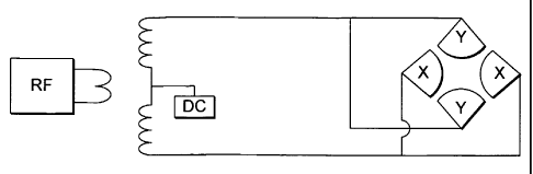
Figure 3 shows a power supply capable of providing the,
desired RF potentials. A RF generator supplies a RF signal
to a primary winding of a transformer, as mentioned above.
This signal is coupled to the secondary winding of the
transformer. One end of the secondary winding is connected
to the x-axis pair of opposed electrodes, the other end is
CA 02572553 2006-12-15
WO 2005/124821 PCT/GB2005/002444
- 3 -
connected to the other, y-axis pair of opposed electrodes.
A DC offset may be applied using a DC supply connected to a
central tap of the secondary winding. AC potentials can
also be applied to the electrodes, but this aspect of the
storage device need not be considered here.
Further details of this type of ion storage device can
be found in U.S. Patent Application Publication No.
2003/0173524.
The inductance in the coils comprising the winding of
the transformer and the capacitance between the electrodes
forms an LC circuit. The transformer corresponds to high
quality resonance coils, with a quality factor reaching many
tens or even hundreds. This produces RF amplitudes up to
thousands of Volts at working frequencies normally in the
range of 0.5-6 MHz.
Such storage devices are often used to store ions prior
to ejection to a subsequent mass analyser. Whenever such
storage devices are interfaced to other analysers,
especially pulsed ones (e.g. to a TOF mass analyser or an
electrostatic-only trapping mass analyser such as the
Orbitrap mass analyser), a problem of efficient transfer of
ions from the storage device to the analyser becomes a
stumbling block. When 3D quadrupole RF traps are used as
storage devices as the first stage of mass analysis, this
problem is traditionally solved by pulsing DC potentials on
end-cups of the ion trap in synchronisation with switching
off the RF signal generator (S.M. Michael, M. Chien, D.M.
Lubman, Rev. Sci. Instrum. 63(10) (1992) 4277-4284). This
normally allows extraction of ions from the ion trap, the
extraction being facilitated by the typically favourable
aspect ratio (i.e. length/width) of the 3D trap. However,
the same factor is also responsible for a limited storage
CA 02572553 2006-12-15
WO 2005/124821 PCT/GB2005/002444
4 -
volume and hence limited space charge capacity of the 3D
trap. Due to the relatively slow and voltage-dependent
switching off transition of RF signal generators, resolving
power (and, presumably, mass accuracy) of the storage device
is severely compromised.
The linear ion trap provides orders of magnitude
greater space charge capacity, but its aspect ratio makes
direct coupling to pulsed analysers very difficult.
Usually, this is caused by the vast incompatability of time
scales of ion extraction from the RF storage device (ms) and
peak width required for pulsed analysers (ns). This
incompatability can be reduced by compressing ions along the
axis and then ejecting ions out axially with high-voltage
pulses (W002/078046). However, space charge effects become
very important in this case.
The above devices use axial ejection, but an
alternative is to eject ions orthogonal to. the axis of the
storage device (see, for example, US5,420,425, US5,763,878,
US2002/0092980 and W002/078046). For this, DC voltages on
opposing rod electrodes are biased in such a way that ions
are accelerated through one electrode into the subsequent
mass analyser. It is also disclosed that the RF potential
on electrodes of the storage device should be switched off
in order to limit energy spread and mass-dependence of ion
energy. However, these disclosures only state the objective
of switching off the RF field at zero phases and do not
describe how this could be done. All of the above
disclosures (except W002/078046) relate only to ion storage
devices using straight electrodes and only in application to
TOFMS.
W000/38312 and W000/175935 describe switching off RF
potentials on the electrodes of a storage device in a 3D
CA 02572553 2006-12-15
WO 2005/124821 PCT/GB2005/002444
- 5 -
trap/TOFMS hybrid mass spectrometer. These documents
disclose switching resonance coils but this has the
disadvantage of requiring power supplies with opposite
polarities, as well as two high-voltage pulsers for each RF
voltage. Large discharge currents impose excessive loads on
these power supplies that can be only partly alleviated by
adding capacitance in parallel. Also, internal capacitance
of pulsers adds to that of the coil thus reducing its
resonant frequency. These disclosures do not show how to
switch RF off on more than one electrode or on multi-filar
coils, or how to combine RF switching with pulsed DC offsets
of electrodes of the RF device. The optimum use of this
scheme is the rapid start of RF voltage rather than rapid
switch-off. Unfortunately, ejection of ions into the
subsequent mass analyser requires high speed of switch-off,
while switch-on could be considerably slower for typically
used quasi-continuous ion sources.
W000/249067 and US2002/0162957 disclose switching RF
off for a 3D trap mass spectrometer (a leak detector) in
order to achieve ion ejection without the use of any DC
pulses. However, these documents do not disclose any viable
schemes of RF switching except conventional powering down of
the primary winding of the coil or use of slow mechanical
relays.
Another example of RF switching for a cylindrical
trap/TOFMS hybrid has been disclosed by M. Davenport et al,
in Proc. ASMS Conf., Portland, 1996, p. 790, and by Q. Ji,
M. Davenport, C. Enke, J. Holland, in J. American Soc. Mass
Spectrom, 7, 1996, 1009-1017. This scheme utilises two fast
break-before-make switches each consisting of two pairs of
MOSFETs (per each phase of RF). The circuit's rating is
limited by the rating of the MOSFETs (900 V), and the
CA 02572553 2006-12-15
WO 2005/124821 PCT/GB2005/002444
6 -
quality of the RF circuit is severely limited by the high
capacitance of the MOSFETs (ca. 100 pF each) that is also
aggravated by the large number of these elements.
Against this background, and from a first aspect, the
present invention resides in a mass spectrometer RF power
supply comprising a RF signal supply; a coil comprising at
least one winding, the coil being arranged to receive the
signal provided by the RF signal supply and to provide an
output RF signal for supply to electrodes of an ion storage
device of the mass spectrometer; and a shunt including a
switch, operative to switch between a first open position
and a second closed position in which the shunt shorts the
coil output.
Providing a shunt that short circuits the coil output
provides a convenient way of rapidly switching the RF signal
supplied to the electrodes of a storage device in a mass
spectrometer. The rapid diversion of current through the
shunt leads to a rapid collapse of the signal in the
secondary winding and, hence, to the RF field generated by
the electrodes. With the RF field in the ion storage device
switched off, the ions can for example be injected into a
mass analyser or the like. Once ions have been ejected, the
switch may be operated again to disconnect the shunt,
thereby removing the short circuit from the secondary
winding. As will be readily understood, this leads to rapid
establishment of a signal in the secondary winding and a RF
field generated by the electrodes, for example.
The coil may comprise a single winding with split
halves. A pump amplifier may be connected between the two
halves, this arrangement providing a RF output from the ends
of the winding that may be supplied to the electrodes.
However, it is currently preferred for the power supply to
CA 02572553 2009-05-21
20086-2302
- 7 -
comprise a transformer, the radio frequency signal supply
being connected to a primary winding of the transformer and
wherein the secondary winding corresponds to the coil. In
this context, the "coil being arranged to receive the signal
provided by the radio frequency signal supply" corresponds
to coupling of-the signal across the windings of the
transformer.
In some embodiments, the power supply further comprises a
full-wave rectifier placed across the soil output, and wherein
the switch is.located on an electrical path linking the coil
output to an output point of the full-wave rectifier. Put
another way, the electrical path including the switch may be
located across a diagonal of the full-wave rectifier. This
diagonal may provide the only return current path of the
rectifier circuit such that there is no complete current
path when the switch is open thereby stopping any current
flow through the shunt, but that. completes a current path
forming the shunt when the switch is closed. Alternatively,
the full-wave rectifier may be placed across the coil output
where the coil comprises a single winding, as-described
above.
Use of a full-wave rectifier circuit is particularly
beneficial as it is envisaged that the switch will be
implemented as a semiconductor switch that is designed to
receive unipolar signals: a rectifier circuit, be it full-
wave or half-wave, provides such a unipolar signal.
Optionally, the secondary winding comprises a
substantially central tap and the switch is located on the
electrical path that extends between the centre tap and the
output point of the full-wave rectifier. In some embodiments,
the secondary winding comprises two symmetrical coils with the
tap being made to the centre portion dividing the two coils,
CA 02572553 2009-05-21
20086-2302
- 8 -
although the exact position of the tap need not be exactly
central. Symmetrical coils are beneficial where the
electrodes receive two-phase voltages as they help to
provide signals of equal magnitude but opposite polarity,.
In some applications, such as in a 3D ion trap, only a
single phase supply may be required. In this case, only a
single secondary winding with no central tap may be used.
In some embodiments, the full-wave rectifier comprises a pair
of diodes. One of the diodes may be connected electrically to
one end of the secondary winding in a forward configuration
thereby conducting current from that end of the secondary
winding but not allowing current flow back to that end of
the secondary winding. The other diode may be connected to
the other end of the secondary winding, also in a forward
configuration such that it conducts electricity from the
other end of the secondary winding but does not allow
current flow back to the other end of the secondary winding.
The other sides of the diode are connected along an
electrical path that contains an output point to which the
electrical path containing the switch is connected. Thus,
this latter electrical path provides a return current path
for the full-wave rectifier.
Although the above description is of a full-wave
rectifier comprising diodes, other components such as
transistors or thyristors may be equally employable.
Due to the electrical currents and voltages used with
the power supply, the switch is preferably a unipolar high-
voltage switch.
Optionally, the power supply further comprises a buffer
capacitance connected to the switch, thereby allowing faster
recovery of RF signals in the secondary winding upon
disconnection of the shunt.
CA 02572553 2009-05-21
20086-2302
9 -
In some embodiments, the transformer is a radio frequency
tuned resonance transformer. Such an arrangement takes advantage
of the LC circuit that is formed by virtue of the inductance
of the coils and the capacitance within the circuit. For
example, the capacitance may be due to the gaps between
electrodes within an ion storage device of the mass
spectrometer.
Optionally, the power supply may further comprise a DC-,
supply connected to the secondary winding, in some embodiments,
connected at a central tap of the secondary winding, that
may provide a DC offset to the signal generated in the
secondary winding. For example, this DC offset could be
used to define ion energy during ion entrance into to the
trap or exit from it. Furthermore, variable DC offsets may
be used.
In some contemplated embodiments of the present
invention, the secondary windings comprise multi-filar
.windings. Such multi-filar == win-in ss -mar comprise two or
more separate coils that, in some embodiments, are located adjacent
one another, thereby forming a close coupling such that the
signal induced across the transformer is present in all
windings of the multi-filar winding. In this configuration,
the shunt need. not he connected to all of the filar windings
and, in some embodiments, is in fact only connected to one of the
filar windings. This is because when the shunt is connected
across one of the filar windings thereby shorting that filar
winding out, the signal collapses in all other coupled filar
windings. In order to form the close coupling, the filar
windings may be located adjacent one another through
juxtaposition (e.g. one beside the other on separate cores)
or they may be interposed (e.g. coils could be wound on a
CA 02572553 2009-05-21
20086-2302
- 10 -
common core such that the windings alternate), or in other
configurations.
In a further contemplated embodiment of the present
invention, a dual RF output may be provided by using a
primary winding comprising a pair of coils that are wound in
opposite senses.
Furthermore, variable and different DC offsets may be
used for different filars, to create a potential well or
potential gradient between electrodes. This potential well
may be advantageous in trapping ions within a storage device
or for their ejection.
from a second aspect, the present invention resides in,
a mass spectrometer comprising an ion source, an ion storage
device, a mass analyser and any of the power supplies
described above; wherein the ion storage device is
configured to receive ions from the ion source and comprises
electrodes operative to store ions therein and to eject ions
to the mass analyser; and the mass analyser is operative to
collect mass spectra from ions ejected by the ion storage
device.
The mass analyser may be of a variety of types,
including electrostatic-only types (such as an Orbitrap
analyser), time-of-flight, FTICR or a further ion trap.
Ions may be ejected from the ion storage device either in
the axial direction (i.e. along the longitudinal axis of the
storage device) or they may be ejected orthogonal to this
axial direction. The ion storage device may be curved so
that it has a curved,longitudinal axis.
From a third aspect, the present invention resides in a
method of operating a mass spectrometer comprising supplying
a RF signal to a coil comprising at least one winding
connected to electrodes of an ion storage device, thereby
CA 02572553 2009-05-21
20086-2302
- 11 -
creating a RF containing field in the ion storage device to
contain ions having a certain mass/charge ratio; and
operating a switch thereby to connect a shunt placed across
the coil output thereby to short out the secondary winding
and to switch off the RF containing field;'or operating a
switch thereby to disconnect the shunt and to switch on the
RF containing field.
Optionally, the coil is a secondary winding of a
transformer of the mass spectrometer and passing the radio
frequency signal to the coil comprises passing an antecedent
radio frequency signal through a primary winding of the
transformer, thereby causing the radio frequency signal to
appear across the secondary winding.
In some embodiments, the method further comprises operating
a switch such that the shunt is connected or disconnected in
synchrony with the phase of the RF signal. This may be
preferable in that the switch is connected and disconnected
controllably at the same time within the phase of the RF
signal. In some cases, it may be preferred to switch the shunt
when the RF signal substantially passes through its average
value. This average value may correspond to zero, although
this need not necessarily be so. For example, a DC bias may
be applied to the RF signal directly.
Optionally, the method further comprises stopping the
RF signal passing through the primary winding when the shunt
is connected across the secondary winding. This connection
and disconnection may be performed as soon as possible after
connection and as soon as possible before disconnection.
Stopping the RF signal may optionally comprise switching a
RF signal generator off, although other options such as
throwing a switch or even providing a further shunt may be
employed.
CA 02572553 2009-05-21
20086-2302
- 12 -
Optionally, the method may further comprise applying a
constant or variable DC offset to the electrodes.
Optionally, the DC offset applied has a fast rise time, i.e.
such that the rise time is'far shorter than the time for all
ions to be ejected from the ion storage device.
Advantageously, this causes the ejected ions to have
energies that are independent of their masses.
Alternatively, the DC offset may be time dependent such that
its magnitude varies to provide ejected ions with energies
related to their mass. For example, continuously ramping or
stepping the DC offset will result in light ions being
ejected with less energy than heavier ions.
The method may optionally comprise switching off the
radio frequency field and then applying the DC offset only
after a delay. Such a method provides beneficial focussing
when ejecting ions to a TOF mass spectrometer. The length
of the delay may be varied to find a value that achieves
optimal focussing.
In some embodiments, the DC offset may be applied to the
secondary windings, optionally to a central tap of the
secondary winding. Applying the DC offset may optionally be
performed to trap ions in the ion storage device or,
alternatively, the DC offset may optionally be used to eject
ions from the storage device. Ejection may be performed
either axially or orthogonally.
Optionally, the method may comprise operating the
switch to switch off the radio frequency containing field;
introducing ions into the ion storage device; and operating
the switch to switch on the radio frequency containing field
thereby to trap ions in the ion storage device. The switch
may be operated to turn on the radio frequency containing
field when the ions approach or arrive at the central axis
CA 02572553 2009-05-21
20086-2302
13 -
of the ion storage device. The ions may be injected
radially into the ion storage device.
In a currently contemplated application of the present
invention, the radio frequency containing field is switched
on to trap ions in the ion storage device, the method
comprising operating the switch to switch off the radio
frequency containing field and, after a short delay,
operating the switch to switch on the radio frequency
containing field; and, during the short delay, introducing
electrons into the ion storage device. The short delay is
chosen such that only minimal, if any, ion loss from the ion
storage device results. For example, the short delay be
chosen to be less than the time taken for ions to drift from
the ion storage device. The method may comprise injecting
low energy electrons into the ion storage device, in which
case the absence of an RF field is beneficial because it
would otherwise excite the electrons to high energy. The
low-energy electrons may be provided for electron-capture
dissociation (ECD).
. Where the ion storage device contains ions trapped by
the radio frequency containing field, the method may
optionally comprise operating the switch to switch off the
radio frequency containing field; and applying DC offsets
selectively to the electrodes thereby to cause ejection of
ions trapped in the ion storage device in a desired
direction. The desired direction may be so as to eject ions
through gaps provided between the electrodes or through
apertures provided in the electrodes.
From a-fourth-aspect.,__the present invention resides in
a method of collecting a mass spectrum comprising operating
an ion source to generate ions; introducing ions generated
by the ion source to an ion storage device; operating the
CA 02572553 2009-05-21
20086-2302
- 14 -
ion storage device according to any of the methods described
above thereby to contain ions in the storage device and to
eject ions to a mass analyser; and operating the mass
analyser to collect a mass spectrum from ions ejected by the
ion storage device.
From a fifth aspect the present invention resides in a
method of collecting a mass spectrum from a mass
spectrometer comprising operating an ion source to generate
ions; introducing ions generated by the ion source to an ion
trap having elongate electrodes shaped to form a central,
curved longitudinal axis; operating the ion trap according
to the method as described above thereby to trap ions and to
eject ions on paths substantially orthogonal to the
longitudinal axis such that the ion paths converge at the
entrance of an electrostatic-only type mass analyser; and
operating the mass analyser to collect a mass spectrum from
ions ejected from the ion trap.
Generally, ions will orbit around the longitudinal axis
following complex paths. These ions are thus ejected in a
direction substantially orthogonal to the longitudinal axis,
i.e. in a direction more or less at right angles to the
points on the longitudinal axis the ion is currently
passing. This direction is towards the concave side of the
ion trap to ensure the many possible ion paths converge.
The curvature of the ion trap and the position of the mass
analyser are such that the ion paths converge at the
entrance to the mass analyser, thereby focussing the ions.
From a sixth aspect, the present invention resides in a computer
readable medium storing a computer program comprising program
instructions that, when loaded into a computer, cause the computer to
control an ion storage device in accordance with any of the methods
described above. Furthermore, from a seventh aspect, the
CA 02572553 2009-05-21
20086-2302
-15-
invention resides in a controller programmed to control an ion storage device
in
accordance with any of the methods described above.
According to one aspect of the present invention, there is provided a
mass spectrometer radio frequency power supply comprising: a radio frequency
signal supply; a coil comprising at least one winding, the coil being arranged
to
receive the signal provided by the radio frequency signal supply and to
provide an
output radio frequency signal for supply to electrodes of an ion storage
device of
the mass spectrometer; and a shunt including a switch, operative to switch
between a first open position and a second closed position in which the shunt
shorts the coil output.
According to another aspect of the present invention, there is provided
a mass spectrometer comprising an ion source, an ion storage device, a mass
analyser and the power supply as described herein; wherein the ion storage
device is configured to receive ions from the ion source and comprises
electrodes
operative to store ions therein and to eject ions to the mass analyser; and
the
mass analyser is operative to collect mass spectra from ions ejected by the
ion
storage device.
According to still another aspect of the present invention, there is
provided a method of operating a mass spectrometer ion storage device,
comprising: supplying a radio frequency signal to a coil comprising at least
one
winding connected to electrodes of an ion storage device, thereby creating a
radio
frequency containing field in the ion storage device to contain ions having a
certain range or ranges of mass/charge ratios; and operating a switch thereby
to
connect a shunt placed across the coil output thereby to short out the coil
output
and to switch off the radio frequency containing field; or operating a switch
thereby
to disconnect the shunt and to switch on the radio frequency containing field.
Examples of embodiments of the present invention will now be
described with reference to the accompanying drawings, in which:
CA 02572553 2009-05-21
20086-2302
- 15a -
Figure 1 is a block diagram representation of a mass
spectrometer,
Figure 2a is-a representation of a linear quadrupole
ion trap and Figures 2b-2d illustrate the DC, AC and RF
voltages used for operation of the ion trap;
Figure 3 shows schematically a circuit for applying RF
and AC voltages to the electrodes of an ion trap;
Figure 4 shows a power supply according to a first
embodiment of the present invention for supplying RF and DC
potentials to electrodes of an ion trap;
Figures 5a and 5b show current flow around the full-
wave rectifier of the power supply of Figure 4;
Figure 6 shows voltage waveforms at present in the
secondary windings of a transformer of the power supply of
Figure 4;
Figures 7a and 7b show DC potentials applied to the
electrodes of Figure 4;
Figures 8a and 8b correspond to Figure 4 but show
second and third embodiments of the present invention;
Figure 9 corresponds to Figure 4 but shows a fourth
embodiment of the present invention;
Figure 10 corresponds to Figure 4 but shows a fifth
embodiment of the present invention; and
Figure lla corresponds to Figure 4 but shows a sixth
embodiment of the present invention, Figure llb shows the
power supply of Figure lla within the context of an Orbitrap
mass analyser, and Figure lic shows the power supply of.
CA 02572553 2006-12-15
WO 2005/124821 PCT/GB2005/002444
- 16 -
Figure lla within the context of time of flight analyser.
A power supply 410 for providing RF and DC potentials
to four electrodes 412, 414 of a linear ion trap is shown in
Figure 4. A RF amplifier 416 provides a RF signal to the
primary winding 418 of a RF-tuned resonance transformer 420.
The transformer 420 comprises a secondary 422 comprised of
two symmetrical windings 424, 426 provided with a central
tap 428 therebetween. The end of the secondary winding 424
remote from the central tap 428 is connected to opposed
electrodes 412 that comprise the upper and lower electrodes
of the ion trap. The end of secondary winding 426 remote
from the central tap 428 is connected to opposed electrodes
414 that form the left and right electrodes of the ion trap.
In addition, a full-wave rectifier circuit 430 is also
connected to the remote ends of secondary windings 424 and
426. The full-wave rectifier 430 comprises two electrical
paths 432 and 434 extending from the remote ends of the
secondary windings 424, 426 that meet at a junction 436.
Each of the paths 432 and 434 are provided with a diode 438
and 440 respectively so as to allow current flow from the
remote ends of the secondary windings 424, 426 but not to
allow current flow back to those remote ends. The junction
436 is connected by a further electrical path 442 to the
central tap 428 of the secondary 422 to form a shunt 442.
This electrical path 442 is provided with a RF-off switch
444 that operates in response to a trigger signal 445. The
switch itself is made using a transistor.
Figure 5a shows the full-wave rectifier 430 with the
switch 444 in an open position. With the switch 444 open,
there is no continuous current loop around the full-wave
rectifier 430 so that there is no current flow. This is
because any current flowing through diode 438 along
CA 02572553 2006-12-15
WO 2005/124821 PCT/GB2005/002444
- 17 -
electrical path 432 cannot flow through switch 444 as
indicated by arrow 446, nor can it flow through the other
reverse-biased diode 440 as indicated by arrow 448.
Similarly any current flowing through diode 440 along
current path 434 cannot flow through switch 444 as indicated
by arrow 450, nor can it flow through the other diode 438 as
indicated by arrow 452. Accordingly, when current flows
through the primary 418, the induced current in the
secondary 422 can only flow to the electrodes 412, 414.
Hence, the RF signal supplied to primary 418 results in a RF
potential on the electrodes 412, 414 thereby creating a RF
field within the ion trap.
Figure 5b shows the full-wave rectifier 430 when switch
444 is closed. In this instance, there is a complete
current path through the rectifier 430. In one phase of the
RF signal supplied to the primary 418, current will flow
through secondary winding 424 to diode 438 along current
path 432. Although this current cannot pass through diode
440, it can return along shunt 442 via switch 444 as
-indicated by the arrow 454. For the other phase of the RF
signal applied to primary 418, current will flow through
secondary winding 426 to diode 440 along electrical path
434. Although the current cannot flow through diode 438, it
returns via shunt 442 and switch 444 as indicated by arrow
456. Accordingly, whatever the phase of the RF signal
supplied to primary 418, a low resistance current path is
formed by the full-wave rectifier 430 that shorts out
current flow through either secondary winding 424 and
electrodes 412 or secondary winding 426 and electrodes 414.
Thus, no RF potential is seen by the electrodes 412, 414 and
the RF field within the ion trap collapses.
CA 02572553 2006-12-15
WO 2005/124821 PCT/GB2005/002444
- 18 -
Clearly, the switch 444 can be operated once more to
return the full-wave rectifier 430 to the configuration
shown in Figure 5a. When this is done, current.can now only
flow through secondary windings 424, 426 via the electrodes
412, 414. Of course, this re-establishes the RF field
within the ion trap.
This operation is reflected in Figure 6 where the
voltage waveform seen by the electrodes 412, 414 is shown.
Initially, the voltage waveform is shown at 610 and
terminates at t1 where switch 444 is closed, thereby
shorting out the secondary windings 412, 414. Switch 444 is
closed as the voltage waveform passes through the zero
value. After a delay, switch 444 is opened at t4 thereby
establishing once more the voltage waveform 612 seen by the
electrodes 412, 414. As will be readily appreciated, the
voltage waveforms 610, 612 may correspond to that seen by
either pair of electrodes 412 or 414. The other pair of
electrodes 412, 414 will see a corresponding but inverted
voltage waveform. As can be seen from Figure 6, switch 444
is opened relative to the phase of the signal being supplied
to the primary 418 such that voltage waveform 612 begins at
the zero crossing.
In addition to the RF potential applied to the
electrodes 412, 414 described above, a DC potential may also
be supplied to the electrodes 412, 414. The DC signal is
supplied by a DC offset supply 458 that is connected to the
central tap 428 of the secondary 422 such that this DC
offset is seen by all electrodes 412, 414. Accordingly, a
DC offset may be added to the RF potential applied to the
electrodes 412, 414 or may alternatively be supplied to the
electrodes 412, 414 when they are not receiving the RF
potential. For example, Figure 6 shows a situation where RF
CA 02572553 2006-12-15
WO 2005/124821 PCT/GB2005/002444
- 19 -
only is supplied to the electrodes 412, 414 such that they
see the voltage signal 610. This creates a RF field within
the ion trap that traps ions for subsequent analysis in a
mass analyser. When ejection of the ions from the ion trap
is desired, the switch 444 is closed at tl thereby shorting
out the secondary 422 and collapsing the RF field in the ion
trap. A short time later at t2, a DC pulse 614 is applied
to the electrodes 412, 414 to create a DC field that ejects
the ions from the ion trap. After sufficient time for all
ions to be ejected, at t3 the DC offset is switched off and
then a short time later at t4, the switch 444 is opened such
that a new RF field is established in the ion trap ready for
trapping further ions. Pulsing the DC waveform 614 will not
cause parasitic oscillations of radio frequency at the
resonant frequency as the secondary 422 is shorted via the
shunt operated by switch 444.
The DC pulse 614 may be used to extract ions
orthogonally from the ion trap. Conventionally, the ions
are extracted through one of the electrodes 412, 414 that
are used to define x and y axes within the ion trap. For
example, the ions may be ejected through one of the
electrodes 414 in the x-direction. Figure 7b shows a linear
DC field that may be created for this extraction, such that
its gradient follows the x-direction. Whilst the RF is
being applied to the electrodes 412, 414, no DC field is
present across electrodes of the ion trap such as that shown
in Figure 7a.
In view of the voltages and currents seen in operation
in the transformer 420, switch 444 corresponds to a unipolar
high voltage switch. The diodes 438 and 440 are selected to
have a low capacitance (typically, a few pF). Accordingly,
this has only minimal effect on the overall capacitance seen
CA 02572553 2006-12-15
WO 2005/124821 PCT/GB2005/002444
- 20 -
by the resonant circuit which is dominated by the
capacitance between electrodes 412, 414. The diodes 438 and
440 may either be individual diodes or a series of diodes
with appropriate current and voltage ratings could be used
instead as conditions dictate. Moreover, switch 444 may be
a single switching device but also could be formed by a
series of semiconductor devices such as MOSFET or bipolar
transistors or thyristors, etc. Examples of multi-
transistor switches are illustrated in the following
embodiments.
The power supply 410 of Figure 4 may be simplified
without departing from the scope of the present invention.
Two such examples are shown in Figures 8a and 8b. As the
embodiments presented in this description contain many
common elements, a numbering convention will be followed
where a number is assigned to a particular feature that is
prefixed by a leading digit that reflects the Figure number.
Hence, the power supply 410 of Figure 4 becomes power supply
810 of Figure 8.
Figure 8a shows a simple embodiment of the invention
that uses a rectifier 838. A power supply 810 for providing
RF potentials to electrode 812 of a quadrupole ion trap is
shown. A RF amplifier 816 provides a RF signal to the
winding of a RF-tuned resonance transformer 810. The end
822 of the transformer 820 remote from a central tap 828 is
connected to electrode 812 of the quadrupole ion trap. A
transistor-based RF-off switch 844 is connected to junction
822 via a diode 838. Though this circuit shorts the coil
only for half-wave, power dissipation could be high enough
to reduce RF amplitude sharply, especially if it is
accompanied with powering down of the RF amplifier 816.
CA 02572553 2006-12-15
WO 2005/124821 PCT/GB2005/002444
- 21 -
Figure 8b shows a simple embodiment of the invention
using a pair of switches 844. A power supply 810 for
providing RF potentials to ring electrode 812 of a
quadrupole ion trap is shown. A RF amplifier 816 provides a
RF signal to the winding of a RF-tuned resonance transformer
820. The end 822 of the transformer 820 remote from the tap
828 is connected to electrode 812 of the quadrupole ion
trap. A pair of transistor-based RF-off switches 844 in
reverse connection bridge across the RF coil 824. This
circuit shunts the coil without the need for any additional
diodes (because the diodes shown in switch 844 are parasitic
ones, being intrinsic to semiconductor switches of the
commonly-used type).
Figure 9 shows a power supply 910 according to a fourth
embodiment of the present invention that ensures more rapid
re-establishment of the RF field in the ion trap when switch
944 is opened to remove the shunt. Figure 9 shares many of
the features of Figure 4. Thus, as mentioned above, like
reference numerals.are used, merely replacing the leading
"4" by a leading "9" so that, for example, switch 444
becomes switch 944.
As can be seen from Figure 6, the voltage waveform 612
that arises on opening the switch 944 has an attenuated
amplitude that increases to reach the amplitude of the
previous voltage waveform 610. This recovery time does in
fact depend upon several parameters, for example the power
of the RF amplifier 916 and the internal capacitance of the
switch 944, among other things. This problem can be
addressed by the inclusion of a further electrical path 960
that runs from the shunt 942 that connects switch 944 to
central tap 928, the electrical path 960 also extending to
the switch 944 that now comprises a pair of semiconductor
CA 02572553 2006-12-15
WO 2005/124821 PCT/GB2005/002444
- 22 -
switches 964 and 966. Shunt 942 extends to semiconductor
switch 966 and electrical path 960 extends to semiconductor
switch 964. The junction 936 on the output side of the
diodes 938 and 940 is connected to both semiconductor
switches 964 and 966, such that switches 964 and 966 control
two return paths. The electrical path 960 is provided with
a buffer capacitance 962 which ensures more rapid recovery
of the RF field in the ion trap on opening the switch 944.
Figure 10 shows a power supply 1010 according to a
fifth embodiment of the present invention. As for Figures
4, 8 and 9, many features are shared and so will not be
described again. The same numbering convention is also
adopted where the leading "4" has now been replaced by a
leading 1110".
The transformer 1020 of Figure 10 comprises a multi-
filar secondary 1022 having a first pair of symmetrical,
connected windings 1024 and 1026, and a second pair of
symmetrical, connected windings 1070 and 1072, wherein the
first and second pair are not connected to each other. Both
the first and second pair of secondary windings are arranged
adjacent one another in juxtaposition such that the RF
signal passing through the primary 1018 induces a RF signal
in both pairs of secondary windings. The first pair of
secondary windings 1024 and 1026 are connected to the full-
wave rectifier 1030 in exactly the same fashion as shown in
Figure 9. That is to say, the full-wave rectifier 1030
includes a buffer capacitance 1062 and is connected to a
switch 1044 comprising two semiconductor switches 1064 and
1066. However, this arrangement need not be employed in
this multi-filar transformer design and instead the single
semiconductor switch 444 of Figure 4 may be employed.
CA 02572553 2006-12-15
WO 2005/124821 PCT/GB2005/002444
- 23 -
The second pair of secondary windings 1070 and 1072 are
connected to the electrodes 1012 and 1014 in a similar
fashion to Figure 4 and Figure 9, i.e. the ends of the
secondary windings 1070 and 1072 remote from a central tap
1074 of the secondary windings 1070 and 1072 are connected
to electrodes 1012 and 1014 respectively.
The DC offset 1058 is connected to the central tap 1074
of the second pair of secondary windings 1070 and 1072.
Moreover, the DC offset 1058 incorporates a more complicated
design in this embodiment, although it is possible to use
the simpler DC offset supply akin to that of Figure 4 or
Figure 9. The DC offset supply 1058 comprises two separate
offsets 1076, 1078 that supply a positive and a negative DC
offset respectively. Either of these offsets 1076 or 1078
can be selected using a pair of transistor switches 1080 and
1082, thereby allowing easy choice of connection of either a
positive or negative DC offset to the field created in the
ion trap.
Figure lla shows a power supply according to a sixth
embodiment of the present invention. This embodiment shows
in more detail an arrangement for providing orthogonal
extraction of ions stored in the ion trap in the x-axis
direction, also shown in Figure lla. To facilitate
extraction, a slot is provided in electrode 1114' as
indicated at 1188. A similar extraction arrangement of a
slot 1188 within an electrode 1114' can be used in any of
the other embodiments. Similar to Figure 9, the embodiment
of Figure lla uses a multi-filar secondary 1122, this time
comprising three pairs of symmetrical secondary windings. A
first pair of symmetrical windings 1124 and 1126 are
connected to the full-wave rectifier 1130. As before,
either the basic switch circuit of Figure 4 may be used or,
CA 02572553 2006-12-15
WO 2005/124821 PCT/GB2005/002444
- 24 -
as is shown in Figure lla, a more complicated switch 1144
including buffer capacitance 1162 may be employed instead.
In the embodiment of Figure lla, each of the four
electrodes are treated separately. Accordingly, they are
now labelled as 1112 and 1112', and 1114 and 1114'. A first
secondary winding 1184 of a second pair of secondary
windings supplies electrode 1112 whereas electrode 1112' is
supplied by a first winding 1170 of a third pair of
secondary windings. Electrode 1114 is supplied by a second
winding 1186 of the second pair of secondary windings
whereas electrode 1114' is supplied by a second winding 1172
of the third pair of secondary windings. As can be seen
from Figure lla, all of the first windings of the first,
second and third pair of secondary windings are connected
together at the central tap 1128 of the first pair of
windings. However, only the second winding 1126 of the
first pair is also connected to the central tap 1128. The
ends of the first of the windings 1172 and 1186 of the
second and third pairs of secondary windings close to the
central tap 1128 are instead connected to a DC offset
supply.
As with Figure 10, positive and negative offsets can be
set from 1176, 1178 that are selectable through a DC offset
switch 1158 comprising two transistors 1180 and 1182.
However, rather than supply these DC offset voltages direct
to secondary windings 1122, they are routed through further
high voltage supply switches 1190 and 1192. These switches
1190 and 1192 that preferably have low internal resistance
may be set such that the DC offsets are delivered direct to
the secondary windings 1122. However, in an alternative
configuration, the switches may be set so that independent
HV offsets can be applied to the two secondary windings 1172
CA 02572553 2006-12-15
WO 2005/124821 PCT/GB2005/002444
- 25 -
and 1186. A push HV supply 1194 supplies a large positive
voltage through push switch 1190 that can be set on
secondary winding 1186 thereby applying a large positive
potential to electrode 1114. This large positive potential
repels ions stored in the ion trap towards the aperture 1188
provided in opposite electrode 1114'. A corresponding pull
HV supply 1196 supplies a large negative potential through-
pull switch 1192 and onto secondary winding 1172, thereby
applying a large negative potential on electrode 1114' that
will attract ions towards its aperture 1188. Accordingly,
this arrangement allows either a small DC offset to be
applied to the electrodes 1112, 1112', 1114, 1114' that may
be used, for example, to provide a potential well for
trapping ions within the ion trap. This potential may even,
for example, be supplied at the same time as the RF
potential being supplied to the electrodes 1112, 1112',
1114, 1114'. When the RF potential is switched off using
switch 1144, ions may be ejected orthogonally from the ion
trap by applying the push 1194 and pull 1196 HV supplies to
the electrodes 1114 and 1114' respectively.
Of course, the circuit of Figure lla may be adapted,
for example, by using only two secondary windings 1122 in
the upper half of the transformer 1120 so that both
electrodes 1112 and 1112' are supplied from a single winding
1170 or 1184.
Also, this idea may be extended such that ions may be
ejected orthogonally from the ion trap, but in any arbitrary
radial direction. This is possible by virtue of the
separate control of each electrode 1112, 1112', 1114, 1114'.
Further push/pull DC offsets may be supplied to electrodes
1112, 1112', such that DC potentials may be set
independently on each electrode 1112, 1112', 1114, 1114' to
CA 02572553 2006-12-15
WO 2005/124821 PCT/GB2005/002444
- 26 -
control the direction of ejection. With suitable choices of
DC offsets, ions may be ejected through the gaps between
electrodes 1112, 1112', 1114, 1114', through aperture 1188
provided in electrode 1114' or through corresponding
apertures provided in the other electrodes 1112, 1112',
1114. A possible application of such an arrangement would
be for multiple ejections to multiple analysers or to other
processing. For example, a first ejection may send some of
the trapped ions along a first path to a mass analyser while
a second ejection may send some of the trapped ions along a
second path to a second analyser or a reaction cell.
Figure llb shows the embodiment of Figure lla applied
to provide compression of ion bunches both in space and in
time. Ions generated in ion source 1200 are introduced from
a linear trap 1201 according to Figure 2 of US5,420,425
through transmission optics (e.g. RF multipole or
electrostatic lenses or a collision cell) into curved
trapping device 1203 with electrodes 1112, 1114 of
essentially hyperbolic shape following the geometry of
Figure 3 of US5,420,425. Ions lose energy in collisions
with bath gas within this trap 1203 and get trapped along
its axis 1205. Voltages on the entrance 1202 and end 1206
apertures of the curved trap 1203 are elevated to provide a
potential well along the axis 1205. These voltages may be
later ramped up to squeeze ions into a shorter thread along
this axis 1205. While RF is switched off and extracting DC
voltages are applied to the electrodes 1112, 1114, these
voltages on the apertures 1202, 1206 stay unchanged. Because
of pulsing the DC offset of all hyperbolic electrodes to
high voltages, resulting potential distribution during the
orthogonal extraction favours divergence of the ion beam
towards apertures 1202, 1206. Nevertheless, extraction
CA 02572553 2006-12-15
WO 2005/124821 PCT/GB2005/002444
- 27 -
occurs so fast that this divergence is kept to minimum. Due
to initial curvature of the trap 1203 and subsequent ion
optics 1207, the ion beam converges on the entrance into the
mass analyser 1208, preferably of the Orbitrap type, similar
to the manner described in Figure 6 of W002/078046.
To improve temporal focusing of ions of the same mass-
to-charge ratio, a delay could be introduced between
switching RF off and pulsing extracting DC voltages. This
will allow ions with higher velocities to move away from the
axis 1205 and provide correlation between ion coordinate and
velocity. As shown in W.C. Wiley, L.H. McLaren, Rev. Sci.
Instrum. 26 (1955) 1150, choosing an appropriate delay
allows a reduction in the time width of the ion beam at a
focal plane at the entrance to the analyser 1208. For an
Orbitrap mass analyser, this improves coherence of ions,
while for TOFMS it improves resolving power directly.
Fast pulsing of DC voltages on the RF secondary 1120
allows all ions to be raised to the desired energy ("energy
lift"). If the rise-time is much smaller than the duration
of ion extraction from the trap 1203, then all ions with the
same m/z ratio will be accelerated approximately by the same
voltage. For injection into the Orbitrap mass analyser 1208,
however, it is preferable that ions with lower m/z values
enter the Orbitrap analyser 1208 at lower energies (as the
trapping voltage is still low) while ions with higher m/z
values enter the analyser 1208 with higher energies. This
could be achieved by reducing the rate of increase of DC
voltages, for example, by installing a resistor between the
switch 1158 and the corresponding RF secondary 1120. Then an
RC-chain is formed by this resistor and the capacitance of
the secondary 1120 (although additional capacitances could
be used if desired) that will determine the rise-time
CA 02572553 2006-12-15
WO 2005/124821 PCT/GB2005/002444
- 28 -
constant of the DC voltage. It could be tuned to provide the
optimum match to the ramp of the central electrode of the
Orbitrap analyser 1208. Also, these time-constants could
differ in order to provide mass-dependant focusing
conditions to compensate for mass-dependant effects of RF
fields.
Figure lic shows a further embodiment of the present
invention. The mass spectrometer of Figure llc largely
corresponds to the spectrometer of Figure lib, except that
the Orbitrap mass analyser 1208 has been replaced by a time
of flight (TOF) analyser 1209. Accordingly, ions exiting
the trap 1203 are focussed by ion optics 1207, formed into a
beam by ion optics 1210, deflected by ion mirror 1211 and
measured by detecting element 1212. The TOF detector 1209
may be of any design.
As will be readily appreciated by those skilled in the
art, the above embodiments are but merely examples and may
be readily varied without departing from the scope of the
present invention.
For example, some of the features of the various
embodiments shown in Figure 4, 8, 9, 10 and 11 may be used
interchangeably. For example, the buffer capacitance 62 is
optional and may be included or excluded from any of the
embodiments shown in those Figures. Furthermore, any of the
various DC offset arrangements may be used. In addition,
choices between single filar windings for the secondary 22
may be changed with the choice of the bi-filar arrangement
of Figure 10 and the tri-filar arrangement of Figure 11 or
any other multi-filar configuration for that matter, as
conditions dictate.
While switches 444; 844; 944; 1044, 1058; 1144, 1158
have been described as being unipolar in the embodiments
CA 02572553 2006-12-15
WO 2005/124821 PCT/GB2005/002444
- 29 -
above, bipolar switches may be used. This allows operation
of the power supply 410; 810; 910; 1010; 1110 with both
positive and negative ions.
The accompanying figures show single diodes 438, 440;
838; 938,=940; 1038, 1040; 1138. 1140. However, these
rectifying diodes may be realised as a group of several
diodes.
Whereas a single primary is shown in the Figures, this
may be changed to produce a dual RF output by using two
primary windings that are wound in opposite senses.
Further modifications could include pulsing ions along
the axis of a straight or curved linear trap; a combination
of the above circuits with additional elements to provide AC
excitation of ions; and so on. The mass analyser may be of
any pulsed type, including FT ICR, Orbitrap, TOFMS, another
trap, but also ions could be transferred into a collision
cell, or any other transmission or reflecting ion optics,
with or without RF fields. In general, any device with ion
manipulation by RF fields could benefit from this invention.
Pulsing of RF off and on could be also used for excitation
of ions, for example when collision-induced dissociation is
desired.
The above circuits may be varied, as will be
appreciated by those skilled in the art, in order to
accommodate multi-section electrodes such as those shown in
Figure 2. This may comprise providing separate power
supplies for each of the front, centre and back sections of
the electrodes or may merely comprise an arrangement that
allows different DC offsets to be applied to the front and
back sections as opposed to the centre section.
The present invention finds application beyond just the
quadrupole ion traps described above. It will be readily
CA 02572553 2006-12-15
WO 2005/124821 PCT/GB2005/002444
- 30 -
apparent to the person skilled in the art that the present
invention may be practised on ion traps with an arbitrary
number of electrodes, such as octapole traps that are well
known in the art.
As will be appreciated, provision of an AC signal to
the electrodes has not been discussed in the above
embodiments but incorporation of such provision will be
straightforward to those skilled in the art.
While the above describes using the shunt primarily to
collapse rapidly the RF field prior to ejection of ions from
the trap, there are also benefits to be gained from the
rapid creation of the field in the ion trap. An example is
the trapping of ions in the ion trap. The shunt may be
operated to short the transformer and switch the RF off
while ions arrive in the trap. Ions may be injected towards.
the central axis of the trap through an aperture in an
electrode (such as aperture 1188) or between electrodes. DC
voltages may be placed on the electrodes to favour
transmission of the ions and focusing towards the axis.
Preferably, the ions are decelerated significantly as they
travel towards the axis. Once the ions of interest have
reached the axis, the DC voltages are pulsed to favour
capture of ions (e.g. all DC voltages are equalised) and the
shunt is used to turn the RF field back on rapidly. Thus,
the ions of interest are captured by the RF field.
A further application for fast switching of the fields
is during electron injection into the ion trap. Ions may be
stored in the ion trap and slow electrons introduced to
cause electron capture dissociation (ECD). RF fields are
undesirable because they makethe injected electrons unstable
and the electrons are lost from the trap as a result. Thus,
the shunt may be used to kill the RF field, a short burst of
CA 02572553 2006-12-15
WO 2005/124821 PCT/GB2005/002444
- 31 -
electrons may then be introduced to react with the ions in
the trap, then the shunt may be used to re-establish the RF
field to trap the fragments. Ideally, the RF field is
collapsed only for a few cycles: this provides enough time
for ECD, but not long enough for ions that their fragments
to drift from the trap.