Note: Descriptions are shown in the official language in which they were submitted.
CA 02572798 2007-01-03
WO 2006/078281 PCT/US2005/014922
SYSTEMS AND METHODS FOR HARVESTING AND INTEGRATING
NANOWIRES
BACKGROUND OF THE INVENTION
Field of the Invention
[00011 The present invention relates to nanowires, and more particularly, to
nanowire harvesting and integration.
Background of the Invention
[0002] Nanomaterials, and in particular, nanowires have the potential to
facilitate a whole new generation of electronic devices. For example, In
certain cases, uses of nanomaterials have been proposed that exploit the
unique and interesting properties of these materials more as a bulk material
than as individual elements requiring individual assembly. For example, Duan
et al., Nature 425:274-278 (September 2003), describes a nanowire based
transistor for use in large area electronic substrates, such as, displays,
anteiuias, and the like that employ a bulk processed, oriented semiconductor
nanowire film or layer in place of a rigid semiconductor wafer. The result is
an electronic substrate that performs on par with a single crystal wafer
substrate that can be manufactured using conventional and less expensive
processes than those used to manufacture poorer performing amorphous
semiconductors, which is also more amenable to varied architectures, such as,
flexible and/or shaped materials.
[0003] In another example, bulk processed nanocrystals have been described
for use as a flexible and efficient active layer for photoelectric devices. In
particular, the ability to provide a quantum confined semiconductor crystal in
a hole conducting matrix (to provide a type-II bandgap offset), allows the
production of a photoactive layer that can be exploited either as a
photovoltaic
device or photoelectric detector. When disposed in an active composite, these
CA 02572798 2007-01-03
WO 2006/078281 PCT/US2005/014922
-2-
nanomaterials are simply processed using standard film coating processes.
See, e.g., U.S. Patent Application No. 10/656,802, filed September 4, 2003,
which is incorporated herein by reference in its entirety.
[0004] In accordance with these uses of nanowires and other nanomaterials,
the new process requirement is the ability to provide a film of nanowires that
are substantially oriented along a given axis. The technology for such
orientation has already been described in detail in, for example,
International
Publication Nos. WO 03/0S5700, WO 03/0S5701 and WO 2004/032191, as
well as U.S. Patent Application No. 10/673,092, filed September 25, 2003,
which all are incoiporated herein by reference in their entirety.
[0005] A major impediment to the emergence of this new generation of
electronic devices based on nanostiuctures is the ability to effectively grow
nanowires and other nanosti-uctures that have consistent characteristics.
Current approaches to harvest and integrate nanowires do not facilitate mass
production, do not yield consistent nanowire perforniance characteristics and
can be improved to generate better device performance based on nanowires.
[0006] What are needed are systems and methods for nanowire harvesting and
integration that facilitate mass production, yield consistent nanowire
perfonnance characteristics and generate improved device performance.
SUMMARY OF THE INVENTION
[0007] The present invention provides methods for harvesting and integrating
nanowires that facilitate mass production, yield consistent nanowire
performance characteristics and generate improved device performance in
devices based on nanowires.
[0008] In a first aspect of the invention, a method is provided for harvesting
nanowires. The method includes providing a first substrate having a first
sacrificial layer deposited thereon, the first sacrificial layer being
selectively
dissolvable relative to a first semiconductor material, growing a population
of
nanowires on the first sacrificial layer, the nanowires comprising the first
CA 02572798 2007-01-03
WO 2006/078281 PCT/US2005/014922
-3-
semiconductor material, and selectively dissolving the sacrificial layer
without
dissolving the nanowires, to release the population of nanowires from the
first
substrate.
[0009] In another aspect, the invention provides a method of harvesting
nanowires, including providing a population of semiconductor nanowires
attached to a surface of a growth substrate, exposing the population of
nanowires to an etchant to remove a sacrificial layer from the population of
nanowires; and harvesting the population of nanowires from the growth
substrate. The sacrificial layer may comprise, for example, an oxide layer,
silicon nitride layer, a layer of photoresist and the like deposited on the
substrate.
[00010] In another aspect of the invention, a method is provided for
depositing
nanowires onto a first surface in a substantially aligned orientation. This
method includes providing the first surface as an outer surface of a cylinder,
placing a portion of the outer surface of the cylinder into contact with a
fluid
suspension of nanowires, and rolling the cylinder to advance different
portions
of the first surface into and out of the fluid suspension of nanowires.
[00011] In a related aspect of the invention, a method for coating nanowires
onto a first surface of a substrate in a substantially aligned orientation is
disclosed. This method includes providing an applicator roller having an outer
surface and an axis, rotating the applicator roller about its axis to place at
least
a poi-tion of the outer surface of the roller into contact with a fluid
suspension
of nanowires, and translating the first surface of the substrate relative to
the
rotating applicator roller to coat the first surface of the substrate with the
fluid
suspension of nanowires.
[00012] The applicator roller can be a part of a standard direct or reverse
gravure coater, for example, or any other suitable coater known to those of
ordinary skill in the art. The applicator roller can be configured to rotate
in
the same or an opposite direction to the direction of movement of the
substrate. The relative motion between the applicator roller and the surface
of
the substrate helps to transfer a consistent amount of nanowire coating
CA 02572798 2007-01-03
WO 2006/078281 PCT/US2005/014922
-4-
material from the roller to the substrate to coat the substrate with
substantially
aligned nanowires. The coating material may consist of nanowires in an
appropriate solvent, or there may be additional stabilizers, binders,
surfactants
etc., which can be used to create a suitable nanowire coating. Metering of the
nanowire coating solution can be accomplished by the gravure roller in a
conventional mamier.
[00013] In a fui-ther aspect, the invention provides a method of depositing
nanowires onto a first surface of a substrate that includes providing a
plurality
of substantially aligned (or unaligned) nanowires iinmobilized within an
aperture disposed through a substrate. Next a second substrate is placed
adjacent to the first surface of the first substrate, and a force is applied
to the
nanowires disposed within the aperture to transfer the nanowires to the first
surface of the first substrate in a substantially aligned fashion.
[00014] In an additional aspect, the invention provides a method of preventing
gate shorts in a nanowire based transistor that includes providing at least a
population of nanowires, wherein a subset of the population of nanowires
spans a source and drain electrode, the population of nanowire comprising a
semiconductor core region extending a length of the nanowire, and a dielectric
shell region extending a length of the nanowire, providing ohmic contact
between the source and drain electrodes and any of the population of
nanowires in contact therewith, differentially etching away the core region of
the nanowire population that is not in olunic contact with the source or drain
electrode; and providing a gate electrode over the population of nanowires,
whereby the gate electrode is not in ohmic contact with the core region of the
population of nanowires.
[00015] Further embodiments, features, and advantages of the invention, as
well as the structure and operation of the various embodiments of the
invention are described in detail below with reference to accompanying
drawings.
CA 02572798 2007-01-03
WO 2006/078281 PCT/US2005/014922
-5-
BRIEF DESCRIPTION OF THE FIGURES
[00016] The invention is described with reference to the accompanying
drawings. In the drawings, like reference numbers indicate identical or
functionally similar elements. The drawing in which an element first appears
is indicated by the left-most digit in the corresponding reference number.
[00017] FIG. 1A is a diagrain of a single crystal semiconductor nanowire.
[00018] FIG. 1 B is a diagram of a nanowire doped according to a core-shell
stnicture.
[00019] FIG. 2A is a diagram of a nanowire based transistor device.
[00020] FIG. 2B is a diagram of a nanowire based transistor device having a
filn7 of oriented nanowires einployed as the conductive channel.
[00021] FIG. 3 schematically illustrates a process for harvesting nanowires
from a growth substrate using a combination of photoresist materials.
[00022] FIGs. 4A-D schematically illustrate a process for harvesting nanowires
(e.g., core-shell nanowire structures) from a growth substrate.
[00023] FIG. 5A illustrates a di-um based system for orienting films of
nanowires onto substrates in which the di-um is positioned horizontally.
[00024] FIG. 5B a diagram of a drum based system for orienting films of
nanowires onto substrates in which the di-um is positioned vertically.
[00025] Figure 6A is a diagram of a reverse gravure coater that can be used to
deposit and align nanowires on a surface of a substrate, e.g., for integration
into a functional device.
[00026] FIG. 6B is an SEM image showing a population of nanowires which
have been substantially aligned on a surface of a substrate using a reverse
gravure coater as shown in FIG. 6A.
[00027] FIG. 7A is a diagram of a gravure coater that includes a "striped"
pattern in which a thin filnz of nanowires is patterned in a series of stripes
on
the coater that are aligned in the direction of web motion of the coater.
[00028] FIG. 7B is a diagram of a substrate (e.g., a flexible, plastic
substrate)
that has been coated using the striped gravure coater of FIG. 7A.
CA 02572798 2007-01-03
WO 2006/078281 PCT/US2005/014922
-6-
[00029] FIG. 8 is a diagram of a slotted or apertured substrate used in the
oriented growth of nanowires for subsequent application.
[00030] FIG. 9 is a diagram of an aperture on a substrate as shown in FIG. 8
that includes substantially oriented nanowires spanning the aperture by having
been grown across the aperture.
[00031] FIG. 10 schematically shows a system and process for transfen-ing
substantially oriented nanowires fi=om an apertured growth substrate to a
receiving substrate, for example, for integration into a functional device.
[00032] FIGs. 11A-11C schematically illustrate processes for preventing gate
shorts in nanowire based transistor devices through the further processing of
nanowires and nanowire films.
DETAILED DESCRIPTION OF THE INVENTION
[00033] It should be appreciated that the particular implementations shown and
described herein are examples of the invention and are not intended to
otherwise limit the scope of the present invention in any way. Indeed, for the
sake of brevity, conventional electronics, manufacturing, semiconductor
devices, and nanowire (NW), nanorod, nanotube, and nanoribbon technologies
and other functional aspects of the systems (and components of the individual
operating components of the systenis) may not be described in detail herein.
Furthermore, for purposes of brevity, the invention is fi=equently described
herein as pertaining to nanowires.
[00034] It should be appreciated that although nanowires are frequently
referred to, the techniques described herein are also applicable to other
nanostructures, such as nanorods, nanotubes, nanotetrapods, nanoribbons
and/or combinations thereof. It should further be appreciated that the
manufacturing techniques described herein could be used to create any
CA 02572798 2007-01-03
WO 2006/078281 PCT/US2005/014922
-7-
semiconductor device type, and other electronic component types. Further,
the techniques would be suitable for application in electrical systems,
optical
systems, consumer electronics, industrial electronics, wireless systems, space
applications, or any other application.
[00035] As used herein, an "aspect ratio" is the length of a first axis of a
nanostiucture divided by the average of the lengths of the second and third
axes of the nanostructure, where the second and third axes are the two axes
whose lengths are most nearly equal to each other. For example, the aspect
ratio for a perfect rod would be the length of its long axis divided by the
diameter of a cross-section perpendicular to (normal to) the long axis.
[00036] The tei-m "heterosti-ucture" when used with reference to
nanostiuctures
refers to nanostructures characterized by at least two different and/or
distinguishable material types. Typically, one region of the nanostiucture
comprises a first material type, while a second region of the nanostnicture
comprises a second material type. In certain embodiments, the nanostnicture
comprises a core of a first material and at least one shell of a second (or
third
etc.) material, where the different material types are distributed radially
about
the long axis of a nanowire, a long axis of an arm of a branched nanocrystal,
or the center of a nanocrystal, for exainple. A shell need not completely
cover
the adjacent materials to be considered a shell or for the nanosti-ucture to
be
considered a heterostructure. For example, a nanocrystal characterized by a
core of one material covered with small islands of a second material is a
heterosti-ucture. In other embodiments, the different material types are
distributed at different locations within the nanostructure. For example,
material types can be distributed along the major (long) axis of a nanowire or
along a long axis of arm of a branched nanocrystal. Different regions within a
heterostructure can comprise entirely different materials, or the different
regions can comprise a base material.
[00037] As used herein, a"nanostructure" is a structure having at least one
region or characteristic dimension with a dimension of less than about 500
im1,
e.g., less than about 200 nm, less than about 100 nm, less than about 50 nni,
or
CA 02572798 2007-01-03
WO 2006/078281 PCT/US2005/014922
-8-
even less than about 20 mn. Typically, the region or characteristic dimension
will be along the smallest axis of the sti-ucture. Examples of such structures
include nanowires, nanorods, nanotubes, branched nanocrystals,
nanotetrapods, tripods, bipods, nanocrystals, nanodots, quantum dots,
nanoparticles, branched tetrapods (e.g., inorganic dendrimers), and the like.
Nanostructures can be substantially homogeneous in material properties, or in
certain embodiments can be heterogeneous (e.g., heterostructures).
Nanoshuctures can be, for example, substantially crystalline, substantially
monocrystalline, polycrystalline, amorphous, or a combination thereof. In one
aspect, eacli of the three dimensions of the nanostructure has a dimension of
less than about 500 nm, for example, less than about 200 mn, less than about
100 mn, less than about 50 nni, or even less than about 20 nm.
[00038] As used herein, the terni "nanowire" generally refers to any elongated
conductive or semiconductive material (or other material described herein)
that includes at least one cross sectional dimension that is less than 500nm,
and preferably, less than 100 nni, and has an aspect ratio (length:width) of
greater than 10, preferably greater than 50, and more preferably, greater than
100.
[00039] The nanowires of this invention can be substantially homogeneous in
material properties, or in certain embodiments can be heterogeneous (e.g.
nanowire heterostilictures). The nanowires can be fabricated from essentially
any convenient material or materials, and can be, e.g., substantially
crystalline,
substantially monocrystalline, polycrystalline, or amorphous. Nanowires can
have a variable diameter or can have a substantially unifoi-m diaineter, that
is,
a dianZeter that shows a variance less than about 20% (e.g., less than about
10%, less than about 5%, or less than about 1%) over the region of greatest
variability and over a linear dimension of at least 5 nm (e.g., at least 10
iun, at
least 20 nm, or at least 50 mn). Typically the diameter is evaluated away from
the ends of the nanowire (e.g. over the central 20%, 40%, 50%, or 80% of the
nanowire). A nanowire can be straight or can be e.g. curved or bent, over the
entire length of its long axis or a portion thereof. In certain embodiments, a
CA 02572798 2007-01-03
WO 2006/078281 PCT/US2005/014922
-9-
nanowire or a portion thereof can exhibit two- or three-dimensional quantum
confinement. Nanowires according to this invention can expressly exclude
carbon nanotubes, and, in certain embodiments, exclude "whiskers" or
"nanowhiskers", particularly whiskers having a diameter greater than 100 nni,
or greater than about 200 im1.
[00040] Examples of such nanowires include semiconductor nanowires as
described in Published International Patent Application Nos. WO 02/17362,
WO 02/48701, and WO 01/03208, carbon nanotubes, and other elongated
conductive or semiconductive sti-uctures of like dimensions, which are
incoiporated herein by reference.
[00041] As used herein, the teim "nanorod" generally refers to any elongated
conductive or semiconductive material (or other material described herein)
similar to a nanowire, but having an aspect ratio (length:width) less than
that
of a nanowire. Note that two or more nanorods can be coupled together along
their longitudinal axis so that the coupled nanorods span all the way between
electrodes. Alteniatively, two or more nanorods can be substantially aligned
along their longitudinal axis, but not coupled together, such that a small gap
exists between the ends of the two or more nanorods. In this case, electrons
can flow from one nanorod to another by hopping fiom one nanorod to
another to traverse the small gap. The two or more nanorods can be
substantially aligned, such that they forni a path by which electrons can
travel
between electrodes.
[00042] A wide range of types of materials for nanowires, nanorods, nanotubes
and nanor-ibbons can be used, including semiconductor material selected fi-om,
e.g., Si, Ge, Sn, Se, Te, B, C (including diamond), P, B-C, B-P(BP6), B-Si, Si-
C, Si-Ge, Si-Sn and Ge-Sn, SiC, BN/BP/BAs, A1N/A1P/AlAs/AlSb,
GaN/GaP/GaAs/GaSb, InN/InP/InAs/InSb, BN/BP/BAs, A1N/A1P/AIAs/AlSb,
GaN/GaP/GaAs/GaSb, InN/InP/InAs/InSb, ZnO/ZnS/ZnSe/ZnTe,
CdS/CdSe/CdTe, HgS/HgSe/HgTe, BeS/BeSeBeTe/MgS/MgSe, GeS, GeSe,
GeTe, SnS, SnSe, SnTe, PbO, PbS, PbSe, PbTe, CuF, CuCI, CuBr, CuI, AgF,
AgCI, AgBr, Agl, BeSiN2, CaCN2, ZnGeP2, CdSnAs2, ZnSnSb2, CuGeP3,
CA 02572798 2007-01-03
WO 2006/078281 PCT/US2005/014922
-10-
CuSi2P3, (Cu, Ag)(Al, Ga, In, TI, Fe)(S, Se, Te)2, Si3N4, Ge3N4, A1203, (Al,
Ga, In)2 (S, Se, Te)3, AIzCO, and an appropriate combination of two or more
such semiconductors.
[00043] The nanowires can also be formed from other materials such as metals
such as gold, nickel, palladium, iradium, cobalt, chromium, aluminum,
titanium, tin and the like, metal alloys, polynlers, conductive polymers,
cerainics, and/or combinations thereof Other now known or later developed
conducting or semiconductor materials can be employed.
[00044] In certain aspects, the semiconductor may comprise a dopant fi=om a
group consisting of: a p-type dopant from Group III of the periodic table; an
n-
type dopant from Group V of the periodic table; a p-type dopant selected from
a group consisting of: B, Al and In; an n-type dopant selected from a group
consisting of: P, As and Sb; a p-type dopant from Group II of the periodic
table; a p-type dopant selected fi=om a group consisting of: Mg, Zn, Cd and
Hg; a p-type dopant fi=om Group IV of the periodic table; a p-type dopant
selected fi=om a group consisting of: C and Si.; or an n-type dopant selected
from a group consisting of: Si, Ge, Sn, S, Se and Te. Other now known or
later developed dopant materials can be employed.
[00045] Additionally, the nanowires or nanoribbons can include carbon
nanotubes, or nanotubes fonned of conductive or semiconductive organic
polymer materials, (e.g., pentacene, and transition metal oxides).
[00046] Hence, although the term "nanowire" is referred to throughout the
description herein for illustrative purposes, it is intended that the
description
herein also encompass the use of nanotubes (e.g., nanowire-like structures
having a hollow tube foimed axially therethrough). Nanotubes can be formed
in combinations/thin fihns of nanotubes as is described herein for nanowires,
alone or in combination with nanowires, to provide the properties and
advantages described herein.
[00047] It should be understood that the spatial descriptions (e.g., "above",
"below", "up", "down", "top", "bottom", etc.) made herein are for purposes of
CA 02572798 2007-01-03
WO 2006/078281 PCT/US2005/014922
-11-
illustration only, and that devices of the present invention can be spatially
arranged in any orientation or mamier.
[00048] Nanomaterials have been produced in a wide variety of different ways.
For example, solution based, surfactant mediated crystal growth has been
described for producing spherical inorganic nanomaterials, e.g., quantum dots,
as well as elongated nanomaterials, e.g., nanorods and nanotetrapods. Other
methods have also been employed to produce nanomaterials, including vapor
phase methods. For example, silicon nanocrystals have been reported
produced by laser pyrolysis of silane gas.
[00049] Other methods employ substrate based synthesis methods including,
e.g., low temperature synthesis methods for producing, e.g., ZnO nanowires as
described by Greene et al. ("Low-temperature wafer scale production of ZnO
nanowire arrays", L. Greene, M. Law, J. Goldberger, F. Kim, J. Johnson, Y.
Zhang, R. Saykally, P. Yang, Angew. Chem. Int. Ed. 42, 3031-3034, 2003),
and higher temperature VLS methods that employ catalytic gold particles, e.g.,
that are deposited either as a colloid or as a thin film that fonns a particle
upon
heating. Such VLS methods of producing nanowires are described in, for
example, Published International Patent Application No. WO 02/017362, the
full disclosure of which is incorporated herein by reference in its entirety
for
all purposes.
Types of Nanowires aiacl Tlaeir Synthesis
[00050] FIG. 1A illustrates a single crystal semiconductor nanowire core
(hereafter "nanowire") 100. FIG. 1 A shows a nanowire 100 that is a uniformly
doped single crystal nanowire. Such single crystal nanowires can be doped
into either p- or n-type semiconductors in a fairly controlled way. Doped
nanowires such as nanowire 100 exhibit improved electronic properties. For
instance, such nanowires can be doped to have carrier mobility levels
comparable to bulk single crystal materials.
CA 02572798 2007-01-03
WO 2006/078281 PCT/US2005/014922
-12-
[00051] FIG. 1B shows a nanowire 110 doped according to a core-shell
structure. As shown in FIG. 1 B, nanowire 110 has a doped surface layer 112,
which can have varying thickness levels, including being only a molecular
monolayer on the surface of nanowire 110.
[00052] The valence band of the insulating shell can be lower than the valence
band of the core for p-type doped wires, or the conduction band of the shell
can be higher than the core for n-type doped wires. Generally, the core
nanostructure can be made from any metallic or semiconductor material, and
the shell can be made fi=om the same or a different material. For example, the
first core material can comprise a first semiconductor selected fi=om the
group
consisting of: a Group II-VI semiconductor, a Group III-V semiconductor, a
Group IV semiconductor, and an alloy thereof. Similarly, the second material
of the shell can comprise a second semiconductor, the same as or different
from the first semiconductor, e.g., selected from the group consisting of: a
Group II-VI semiconductor, a Group III-V semiconductor, a Group IV
semiconductor, and an alloy thereof. Example semiconductors include, but
are not limited to, CdSe, CdTe, InP, InAs, CdS, ZnS, ZnSe, ZnTe, HgTe,
GaN, GaP, GaAs, GaSb, InSb, Si, Ge, AlAs, AlSb, PbSe, PbS, and PbTe. As
noted above, metallic materials such as gold, clu=omium, tin, nickel, aluminum
etc. and alloys thereof can be used as the core material, and the metallic
core
can be overcoated with an appropriate shell material such as silicon dioxide
or
other insulating materials
[00053] Nanostilictures can be fabricated and their size can be controlled by
any of a number of convenient methods that can be adapted to different
materials. For example, synthesis of nanocrystals of various composition is
described in, e.g., Peng et al. (2000) "Shape Control of CdSe Nanocrystals"
Nature 404, 59-61; Puntes et al. (2001) "Colloidal nanocrystal shape and size
control: The case of cobalt" Science 291, 2115-2117; USPN 6,306,736 to
Alivisatos et al. (October 23, 2001) entitled "Process for forming shaped
group III-V semiconductor nanocrystals, and product fonned using process";
USPN 6,225,198 to Alivisatos et al. (May 1, 2001) entitled "Process for
CA 02572798 2007-01-03
WO 2006/078281 PCT/US2005/014922
-13-
foiming shaped group II-VI semiconductor nanocrystals, and product formed
using process"; USPN 5,505,928 to Alivisatos et al. (April 9, 1996) entitled
"Preparation of III-V semiconductor nanocrystals"; USPN 5,751,018 to
Alivisatos et al. (May 12, 1998) entitled "Semiconductor nanocrystals
covalently bound to solid inorganic surfaces using self-assembled
monolayers"; USPN 6,048,616 to Gallagher et al. (April 11, 2000) entitled
"Encapsulated quantum sized doped semiconductor particles and method of
manufacturing same"; and USPN 5,990,479 to Weiss et al. (November 23,
1999) entitled "Organo luminescent semiconductor nanocrystal probes for
biological applications and process for making and using such probes."
[00054] Growth of nanowires having various aspect ratios, including nanowires
with controlled dianieters, is described in, e.g., Gudiksen et al (2000)
"Diameter-selective synthesis of semiconductor nanowires" J. Am. Chem.
Soc. 122, 8801-8802; Cui et al. (2001) "Diameter-controlled synthesis of
single-crystal silicon nanowires" Appl. Phys. Lett. 78, 2214-2216; Gudiksen et
al. (2001) "Synthetic control of the diameter and length of single crystal
semiconductor nanowires" J. Phys. Chem. B 105,4062-4064; Morales et al.
(1998) "A laser ablation method for the synthesis of crystalline semiconductor
nanowires" Science 279, 208-211; Duan et al. (2000) "General synthesis of
compound semiconductor nanowires" Adv. Mater. 12, 298-302; Cui et al.
(2000) "Doping and electrical transport in silicon nanowires" J. Phys. Chem.
B 104, 5213-5216; Peng et al. (2000) "Shape control of CdSe nanocrystals"
Nature 404, 59-61; Puntes et al. (2001) "Colloidal nanocrystal shape and size
control: The case of cobalt" Science 291, 2115-2117; USPN 6,306,736 to
Alivisatos et al. (October 23, 2001) entitled "Process for forniing shaped
group III-V semiconductor nanocrystals, and product for-nied using process";
USPN 6,225,198 to Alivisatos et al. (May 1, 2001) entitled "Process for
forming shaped group II-VI semiconductor nanocrystals, and product formed
using process"; USPN 6,036,774 to Lieber et al. (March 14, 2000) entitled
"Method of producing metal oxide nanorods"; USPN 5,897,945 to Lieber et
al. (April 27, 1999) entitled "Metal oxide nanorods"; USPN 5,997,832 to
CA 02572798 2007-01-03
WO 2006/078281 PCT/US2005/014922
-14-
Lieber et al. (December 7, 1999) "Preparation of carbide nanorods"; Urbau et
al. (2002) "Synthesis of single-crystalline perovskite nanowires composed of
barium titanate and strontium titanate" J. Am. Chem. Soc., 124, 1186; and
Yun et al. (2002) "Ferroelectric Properties of Individual Barium Titanate
Nanowires Investigated by Scaiuled Probe Microscopy" Nanoletters 2, 447.
[00055] Growth of branched nanowires (e.g., nanotetrapods, tripods, bipods,
and branched tetrapods) is described in, e.g., Jun et al. (2001) "Controlled
synthesis of multi-armed CdS nanorod architectures using monosurfactant
system" J. Am. Chem. Soc. 123, 5150-5151; and Mamla et al. (2000)
"Synthesis of Soluble and Processable Rod-,Arrow-, Teardrop-, and Tetrapod-
Shaped CdSe Nanocrystals" J. Am. Chem. Soc. 122, 12700-12706.
[00056] Synthesis of nanoparticles is described in, e.g., USPN 5,690,807 to
Clark Jr. et al. (November 25, 1997) entitled "Method for producing
semiconductor particles"; USPN 6,136,156 to El-Shall, et al. (October 24,
2000) entitled "Nanoparticles of silicon oxide alloys"; USPN 6,413,489 to
Ying et al. (July 2, 2002) entitled "Synthesis of nanometer-sized particles by
reverse micelle mediated techniques"; and Liu et al. (2001) "Sol-Gel Synthesis
of Free-Standing Ferroelectric Lead Zirconate Titanate Nanoparticles" J. Am.
Chem. Soc. 123, 4344. Synthesis of nanoparticles is also described in the
above citations for growth of nanocrystals, nanowires, and branched
nanowires, where the resulting nanostructures have an aspect ratio less than
about 1.5.
[00057] Synthesis of core-shell nanostructure heterostructures, namely
nanocrystal and nanowire (e.g., nanorod) core-shell heterostructures, are
described in, e.g., Peng et al. (1997) "Epitaxial growth of highly luminescent
CdSe/CdS core/shell nanocrystals with photostability and electronic
accessibility" J. Am. Chem. Soc. 119, 7019-7029; Dabbousi et al. (1997)
"(CdSe)ZnS core-shell quantum dots: Synthesis and characterization of a size
series of highly luminescent nanocrysallites" J. Phys. Chem. B 101, 9463-
9475; Maima et al. (2002) "Epitaxial growth and photochemical annealing of
graded CdS/ZnS shells on colloidal CdSe nanorods" J. Ain. Chem. Soc. 124,
CA 02572798 2007-01-03
WO 2006/078281 PCT/US2005/014922
-15-
7136-7145; and Cao et al. (2000) "Growth and properties of semiconductor
core/shell nanocrystals with InAs cores" J. Am. Chem. Soc. 122, 9692-9702.
Similar approaches can be applied to growth of other core-shell
nanostructures.
[00058] Growth of nanowire heterostructures in which the different materials
are distributed at different locations along the long axis of the nanowire is
described in, e.g., Gudiksen et al. (2002) "Growth of nanowire superlattice
structures for nanoscale photonics and electronics" Nature 415, 617-620;
Bjork et al. (2002) "One-dimensional steeplechase for electrons realized"
Nano Letters 2, 86-90; Wu et al. (2002) "Block-by-block growth of single-
crystalline Si/SiGe superlattice nanowires" Nano Letters 2, 83-86; and US
patent application 60/370,095 (April 2, 2002) to Empedocles entitled "
Nanowire heterostructures for encoding information." Similar approaches
can be applied to growth of other heterostiuctures.
ExeinplaT:v Naiaowire Devices
[00059] Exemplary applications of semiconductor nanmvire materials include
simple electronic components, such as, transistors. For example, a simple
nanowire transistor device is shown in FIG. 2A. As showYl, the basic device
200 includes a source electrode 202 and a drain electrode 204 disposed upon a
substrate 206 and spaced apart from each other. A semiconductor nanowire
208 is provided spamling the two electrodes and is electrically connected to
the electrodes 202 and 204. The transistor typically includes an insulator or
dielectric layer over its surface that provides insulation between the
nanowire
208 and, for exaniple, gate electrode 210. As shown, the dielectric layer is
provided as an oxide shell 212 or coating on the nanowire 208. By
modulating the field applied to the gate electrode 210, one can vary the
conductivity of the nanowire 208 as in a conventional field effect transistor
(FET).
CA 02572798 2007-01-03
WO 2006/078281 PCT/US2005/014922
-16-
[00060] FIG. 2B schematically illustrates a variation of the simple device
shown in FIG. 2A. As shown, the transistor device 250 includes source 252,
drain 254 and gate 260 electrode provided upon a substrate 256. However, in
place of a single nanowire with a dielectric shell is a film or population of
substantially oriented nanowires 258 that span the source and drain electrodes
252 and 254, bridging the gate electrode 260. As compared to the device
illustrated in FIG. 2A, the nanowire film 258 provides a much higher current
density than a single nanowire based device, while retaining processibility
advantages of film-based processing and uniformity. In particular, the fact
that some of the nanowires in the nanowire population do not completely span
the source and drain electrodes does not substantively affect the operation of
the device as the overwhehning number of nanowires will provide this
functionality.
Sacrificial Layers and Othei- Methocls for Harvesting NalaOwires
[00061] Once synthesized, for many applications, it is necessary to separate
the
nanowires from the substrate from which they are grown. For exanlple, in
certain nanowire applications, it is desirable to provide nanowires deposited
as
a thin film of wires over a flat substrate surface (See, e.g., Published
International Patent Application No. 2004/032193, and Duan et al., Nature
425:274-278 (September 2003)). Accordingly, it is desirable to be able to
unifoimly remove nanowires from the growth substrate, e.g., without
randomly breaking the wires upon removal. In this respect, the invention
provides methods of incorporating a release layer in the growth substrate,
that
can be activated to release the wires from the surface unifonnly and without
any extraneous mechanical disruption that may cause uneven breakage or the
like.
[00062] In a particular aspect, a sacrificial layer is deposited upon or other
wise
provided upon the growth substrate. By sacrificial layer, is meant a layer
that
can be selectively removed or altered to allow facile removal of the nanowires
CA 02572798 2007-01-03
WO 2006/078281 PCT/US2005/014922
- 17-
that are attached thereto without the need for mechanical removal methods, for
example, scraping, shearing or the like. By way of example, a sacrificial
layer
may include a layer that is selectively etchable without damaging the wires
attached to it.
[00063] For example, where silicon nanowires are grown, the underlying
substrate may be provided with, e.g., a silicon nitride layer. The silicon
nitride
layer may be selectively etched using, e.g., orthophosphoric acid, which
etches
the nitride layer without attacking the silicon nanowires. Depending upon the
composition of the synthesized wires, a variety of different sacrificial
layers
may be employed, provided they can be differentially treated to release the
wires without damaging them. Such materials include, for example, oxide
layers, metal layers, or the like, which may react differently to various
etchants or other chemicals than semiconductor wires, for example, silicon.
[00064] Some exemplary wire/release layer pairs include, for example, Si
nanowires grown from an Si02 substrate having a tungsten or molybdemum
sacrificial layer over the Si02 substrate. This metal layer can generally be
differentially etched using buffered, mildly alkaline fei-ricyamiide-based
etchant fomiulations that are generally coinmercially available. Likewise, SiN
layers may be used between a Si02 substrate and Si nanowires. Such
sacrificial layers may generally be etched using phosphoric acid, e.g., 85% by
weight. The sacrificial layer may be crystalline (and/or teinplated on a
crystalline substrate) to generate templated vertical nanowire growth. For
example, atomic layer deposition (ALD) may be used to deposit a thin film of
a catalyst material over a sapphire substrate, where the thin film retains the
crystal periodicity of the sapphire, but is differentially etchable compared
to
sapphire and the nanowires.
[00065] In other embodiments of the invention for uniformly removing
nanowires from the growth substrate, for example, without randomly breaking
the wires upon removal, there are disclosed methods for releasing nanowires at
their base, for example, by selectively etching the base portion of the
nanowires. In this respect, the invention provides methods of selectively
CA 02572798 2007-01-03
WO 2006/078281 PCT/US2005/014922
- 18-
exposing the base portion of the nanowires, and chemically (or mechanically,
ultrasonically, etc.) releasing (e.g., by etching) the base portion to remove
the
wires from the surface uniformly and without any extraneous mechanical
disruption that may cause uneven breakage or the like.
[00066] For example, with reference first to FIG. 3, a first embodiment is
shown in which a conunonly used photoresist material 302 is first deposited
(e.g., spin coated) on the substrate (e.g., a Si substrate) to coat the end
portions
303 of the nanowires 304 proximate a surface of the substrate 300. Any
excess photoresist inadvertently deposited on the sidewalls of the nanowires
can be removed using, for example, one or more commercially available
photoresist solvents or chemicals and/or dry oxygen plasma etching.
[00067] A second layer of a different photoresist material 306, which can be
differentially etched fi=om the first photoresist material 302, may then be
patterned on the sidewalls of the nanowires. The surface of the nanowires
may optionally be functionalized, for example, with standard silane
chemistries or other chemical moieties to attract the second photoresist
material 306 (e.g., a hydrophobic polyiner such as polyvinylidene fluoride
(PVDF)) that would adhere to the nanowires, and not the photoresist 302 on
the substrate.
[00068] The photoresist 302 on the substrate may then be removed with
standard chemicals or solvents and/or by plasma etching to expose the end
poi-tions 303 of the nanowires.
[00069] The exposed end portions of the nanowires attached to the substrate
may then be etched with an etchant such as HF/HNO3, for example, for silicon
nanowires, to release and remove the nanowires resulting in fi=eestanding
nanowires of substantially uniform length.
[00070] The nanowires can be removed as grown (e.g., without an oxide and/or
metal shell coating), or can be removed after a post-growth oxidation (or
other
process step) to foi-m one or more shell layers (e.g., a dielectric or metal
gate
layer) on the nanowire core (as described further below). In the latter case,
a
separate HF etch or metal etch step may also be required to completely
CA 02572798 2007-01-03
WO 2006/078281 PCT/US2005/014922
-19-
remove one or more of the shell layers such as a dielectric or conductive
metal
(e.g., gate) layer.
[000711 The photoresists used in this process are relatively easy to coat and
easy to dissolve. The process is compatible with most of the materials and
processes used in existing microfabrication technology, such as doping the
wires directly on the growth substrate prior to release and deposition on a
device substrate.
[00072] In another embodiment for releasing nanowires fi=om the growth
substrate is shown in FIGs. 4A-D, a process flow is shown for growing and
releasing core-shell nanowire stiuctures from a growth substrate 401. This
process flow involves multi-layer core-shell nanowires containing, for
example, a semiconducting core chosen to provide the desired electronic
functionality (e.g., CMOS compatibility, RF signal processing capabilities,
light emission, etc.), a gate-dielectric inner-shell and a gate-electrode
conductive outer-shell.
[00073] The first shell is an insulating dielectric layer that acts as the
gate-
dielectric in the final device. When employed, the outer layer is a conductive
layer that acts as a conformal gate electrode around each individual wire in
the
final device. Such multi-layer (and single) core-shell nanowires are further
described, for example, in co-pending U.S. Patent Application Ser. No.
10/674,071 entitled "Applications of Nano-enabled Large Area
Macroelectronic Substrates," filed September 30, 2003, the entire contents of
which are incoiporated by reference herein.
[00074] In this embodiment, following growth of core nanowires 400 (e.g.,
using VLS epitaxial growth to grow core Si nanowires, for example, by
decoinposing SiC14 at around 900 degrees C in a CVD furnace on a<111> Si
wafer properly coated with Au or Pt colloids or thin film patterns), the
nanowires are exposed to an etchant (e.g., HF vapor) to remove the native
(amorphous) oxide layer. Removal of the native oxide layer is perfonned if
the thin native oxide layer is not of sufficient quality to withstand a high
CA 02572798 2007-01-03
WO 2006/078281 PCT/US2005/014922
-20-
electric field used in device applications such as macroelectronic
applications.
[00075] The native oxide layer can be replaced with a high quality dielectric
material layer 402 (e.g., a silicon oxide shell) generated by either
controlled
thennal oxidation or chemical vapor deposition, for example. Dielectric
material layer 402 can be chosen from a variety of dielectric materials, such
as
Si02 or Si3N4. The dielectric material layer 402 can be formed by oxidizing
the nanowire, coating the nanowire, or otherwise forming the dielectric layer.
Other non-oxided high dielectr-ic constant materials can be used, including
silicon nitride, Ta205, Ti02, Zr02, Hf02, A1203, and others. Nitridation of
nanowires can be accomplished with processes similar to those employed in
oxidation of nanowires. These materials can be applied to nanowires by
chemical vapor deposition (CVD), solution phase over-coating, or simply by
spin-coating the appropriate precursor onto the substrate. Other known
techniques can also be employed, as would be apparent to persons of skill in
the relevant arts.
[00076] Next, as shown in FIG. 4A, a gate electrode outer shell layer 404 of a
conductive material such as WN, W, Pt, highly doped silicon etc., which is
preferably able to withstand high processing temperatures (e.g., on the order
of
about 1000 degrees C), is deposited on the inner dielectric material layer
402,
for exaniple, by atomic layer deposition (ALD) or other confoimal deposition
process. The outer shell layer 404 is a conductive layer that acts as a
conformal gate electrode around each individual wire in the final device.
[00077] This deposition step is followed by a directional etch step to etch
portions of the outer shell layer 404 overlaying the substrate 401 as shown in
FIG. 4B. This can be accomplished, for example, by using physical etching
such as ion mill etching or reverse-sputtering, or by chemical etching with
appropriate wet chemical etchants such as phosphoric, hydrochloric, nitric,
and/or acetic acids or others known to those of ordinary skill in the art.
Subsequently, the substrate is exposed to a buffered oxide etch (BOE) vapor
or wet solution for approximately between about 10 seconds to 60 seconds, or
CA 02572798 2007-01-03
WO 2006/078281 PCT/US2005/014922
-21-
for example, between about 10 seconds to 30 seconds, to remove the exposed
oxide layer 402 from the substrate surface and fi=om the exposed end portions
on the nanowires as shown in FIG. 4C.
[00078] The exposed base portion 406 of the nanowire 400 may then be etched,
for example, by dipping the growth substrate into a wet Si etch bath, or by
suitable BOE etch (e.g., following selective oxidization after removal of the
dielectric layer from the growth substrate and the exposed end portions of the
nanowires in FIG. 4C).
[00079] The Si acid bath has the advantage of etching the Si core wire inside
the shell layers 402, 404 as shown in FIG. 4D which can help prevent shorts to
deposited metals or to the outer conductive shell layer 404 when the nanowires
are incoiporated into device structures such as FET's, diodes and the like.
Etching the exposed end portions of the nanowires releases them from the
growth substrate as shown in FIG. 4D. The growth substrate may then be
removed from the acid bath, or the acid bath neutralized with suitable alkali
chemicals to stop the etching process. The removed nanowires may then be
dispersed in solution and made available for deposition/coating onto a
suitable
device substrate as described further below.
[00080] It is to be appreciated that the above described process can be
applied
to other nanowire materials and other core-shell structures as well, including
simpler single core-shell structures as well as three layer, four layer, and
additional multi-layer core-shell structures. The doping and doping type of
the
core-shell structure can be flexibly changed and controlled during the growth
process as well to obtain desired properties.
In.tegration of Naizolvires iiato Devices
[00081] Following synthesis and release of nanowires from growth substrates,
many applications require the controlled deposition of the free nanowires onto
another substrate, for example, upon an electronic substrate, connecting
electrical contacts, etc. For example, in certain cases, it is desirable to
provide
CA 02572798 2007-01-03
WO 2006/078281 PCT/US2005/014922
-22-
filnis of nanowires deposited upon a substrate and positioned in particular
locations and/or oriented substantially along a one or more particular axes. A
number of methods have been previously described for depositing and
aligning or orienting nanowires on a substrate, including flow based alignment
where fluids carrying nanowires are flowed over the substrate. Alternatively
methods that utilize adhesive patches to stick and stretch the nanowires into
a
desired orientation have also been described. In accordance with the present
invention, a modification to a typical flow based alignment method, for
example, as described in published U.S. Patent Application No. 2003/186522,
which is incorporated herein by reference, is envisioned.
[00082] In particular, previously described flow-based orientation methods
applied a chaiuiel or other fluid conduit over the desired portion of the
substrate upon which oriented wires were to be deposited. The surface was
typically treated with a chemical moiety that facilitated wire adhesion or
association. When flowed tlirough the channel, the wires tend to align along
the streamlines of the flowing fluid, thus orienting in the direction of flow.
While veiy effective, this type of orientation method required the use of
fluid
channel blocks, etc., and was better suited for small scale.
[00083] The present invention, however, employs a process that is much better
suited to larger scale production of oriented nanowire films or substrates. h1
a
particular embodiment, a fluid suspension of nanowires is deposited into a
rolling drum. Typically, the drum is oriented sideways, so as to permit a much
smaller volume of fluid to be used, but still allow uniform coating of a
portion
of the drum or the entire drum. A substrate, for example, flexible substrate,
is
then wrapped around a smaller inner drum which is disposed within the larger
drum, so that a portion of the substrate's surface is in contact with the
fluid
suspension of wires. The drum is then turned so that the suspension flows
over the surface of the substrate. This flowing provides the same level of
orientation as previously described methods, but does so over a larger
substrate area of a flexible material. Although illustrated with a flexible
substrate, it will be appreciated that small rigid substrates may be used as
well,
CA 02572798 2007-01-03
WO 2006/078281 PCT/US2005/014922
- 23 -
provided their surfaces are in contact with the fluid in the rolling drum at
some
point during the rotation.
[00084] In alternative an=angements, the drums may be oriented in an upright
orientation, with the fluid suspension sandwiched between the substrate and
the outer wall of the larger drum. Both exemplary configurations are
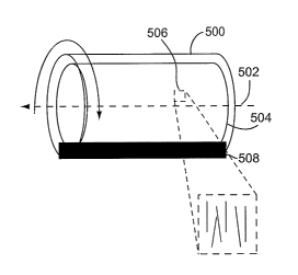
illustrated in FIGs. 5A and 5B. As shown in FIG 5A, a main drum 500 is
provided on a horizontal axis or axle 502 so as to permit rotation. A small
dnlm 504 is inserted into the larger drum 500. In some cases, the smaller
di-um 504 may be fixedly coupled to the same axle 502 as the larger drum 500,
or actually joined to the larger drum 500, so that both dnims rotate together.
However, as noted previously, in certain cases, it is desirable to permit
independent rotation of the two dnims. As such, the inner drum 504 may be
coupled to a separate axle or may simply be independent from and on separate
bearings fi=om the larger di-um 500, so that it can rotate freely. The
substrate
506 is placed on the outer surface of imler dntm 504 inside larger drum 500.
[00085] A small amount of a fluid nanowire suspension 508 is provided in the
larger drum, in sufficient amount to allow contact of the substrate 506 with
the
fluid 508.
[00086] FIG. 5B illustrates a similar embodiment, but where the imler and
outer drums 500 and 504 are placed upon a vertically oriented axle 502. In
this case, it may be desirable to provide a smaller amount of space between
the
two drums, so as to minimize the amount of fluid used.
[00087] Following rotation through the fluid suspension of nanowires 508, the
wires in solution will be deposited upon the surface of the substrate 506 in a
substantially oriented fashion, as a result of the flow based contact, as
shown
in the expanded view seginent of substrate 506. Flow based methods of
nanowire alignment and orientation on substrates are described in Published
U.S. Patent Application No. 2003/186522, previously incorporated herein by
reference.
[00088] In a related aspect of the invention, a gravure coater as shown in
FIG.
6A can be used to facilitate large scale production of oriented nanowire films
CA 02572798 2007-01-03
WO 2006/078281 PCT/US2005/014922
-24-
on substrates. In this embodiment, a main applicator roller or drum 600 is
provided on a horizontal axis or axle 602 so as to permit rotation through a
solution of nanowires 604. Second impression rollers or drums 606 are
located on opposite sides of main roller 600 and are configured to rotate in
either in the same or opposite direction as main roller 600 on horizontal axes
or axles 608. The substrate 610 to be coated passes around the impression
rollers 606, and is coated by the nanowire solution in a nip 612 formed
between roller 600 and substrate 610.
[00089] Following rotation of the main applicator roller 600 through the fluid
suspension of nanowires 604, the wires in solution will be deposited upon the
surface of the substrate 610 in a substantially oriented fashion as shown by
reference to FIG. 6B, as a result of the flow based contact and shearing
motion
between the substrate and gravure roller surfaces. The relative motion helps
to
transfer a consistent amount of nanowire coating material fi=om the gravure
applicator roller 600 to the substrate 610 to coat the substrate with
substantially aligned nanowires.
[00090] The coating material may consist of nanowires in an appropriate
solvent, or there may be additional stabilizers, binders, surfactants etc.
which
can be used to create a suitable nanowire coating. Metering of the nanowire
coating solution can be accomplished by the gravure roller in a conventional
mamier.
[00091] It is to be appreciated that other types of coaters other than direct
or
reverse gravure coaters can be used for applying roll coatings of nanowires to
a surface of a substrate including without limitation rod coaters,
differential
offset gravure coaters, micro gravure coaters, reverse roll coaters, 3-roll
coaters, saturation coaters, hot melt coaters, split film coaters, knife
coaters,
dip coaters, slot die coaters, slide coaters, doctor blade coaters, Meyer rod
and
Meyer rod related coaters, and other roll coaters which are well know to those
of ordinary skill in the art. A variety of coating processes may also be used
such as, for example, hot melt coating, pressure sensitive coating, PVC resin,
doctor blade hand drawdown or Meyer rod coating, and other coating
CA 02572798 2007-01-03
WO 2006/078281 PCT/US2005/014922
- 25 -
techniques or machines by which a liquid flow can be generated during the
coating to achieve proper nanowire alignnient.
[00092] In macroelectronic and other applications, electronic components may
be sparsely arrayed over select portions of a substrate surface. For example,
co-pending and commonly assigned U.S. patent application Serial No.
10/674,060, titled "Large-Area Nanoenabled Macroelectronic Substrates And
Uses Therefor", filed September 30, 2003 describes methods and systems for
high-performance large-area thin-film electronics that provide the electronic
perfoimance of a silicon wafer, but can be processed over large areas, at low-
temperature, on flexible plastic substrates. The substrates described therein
incoiporate thin films of semiconducting nanowires deposited therein and
configured to operate as transistors (or other electronic devices such as
diodes
and the like). hl such applications, nanowires are only needed at certain
locations where the semiconductor devices (e.g., transistors, diodes etc.) are
to
be formed. Nanowires used for fabrication of these electronic components can
be unifoi7nly deposited on the surface of the substrate, but any nanowires not
actually incoiporated into the electronic devices are "wasted." It is possible
that these extraneous wires could be removed and recycled to reduce cost, but
a more direct cost savings could be realized with a patterned deposition
process, in which the extraneous nanowires are not deposited at all.
[00093] In web-based (e.g., roll-to-roll) processing applications, a thin film
of
nanowires can be patterned on a device substrate, for exaniple, by using a
gravure coater 700 having a "striped" pattern in which a film of nanowires is
patterned in a series of stripes 702 that are aligned in the direction of web
motion as shown in FIGs 7A and 7B. The use of such a striped gravure coater
700 provides a striped pattern of nanowires 712, corresponding to series of
stripes 702, on a device substrate 704 used in a nanowire-based device, as
shown in Figure 7B. The savings in nanowires is governed by the stripe pitch
and width, for example, a stripe width of 100 microns with a pitch of 1 mm
may allow a 75% to 90% (or more) reduction in nanowire usage.
CA 02572798 2007-01-03
WO 2006/078281 PCT/US2005/014922
-26-
[00094] Striping with a web coater such as a gravure coater can be realized in
a
number of ways to provide alternating smooth and textured regions (e.g.,
con=esponding to non-deposition and deposition regions, respectively) to
deposit aligned nanowires in stripes where they are needed. If a gravure
coater (e.g., a direct or reverse gravtue coater as described above) is used,
which has the advantage of aligning the nanowires, the striping can be
accomplished by, for example, texturing only the part of the gravure roller
700
where stripes are to be located, or by lyophobic treatment of the gravtire
roller
in the area between stripes. With slot coating, the slot can be closed between
the stripes. Alternatively, the nanowire deposition can be uniforni, but
striping
occurs with a patterned doctor-blade or Meyer rod down-web of the
deposition.
[00095] Furthermore, according to other aspects of the present invention,
nanowires can be deposited from solution in specific, patterned locations on
large area substrates using low-cost, low-temperature processes including
micro-contact, offset or ink jet printing technology, for example. In one
embodiment, for example, ink jet printing technology can be used to both
pattern nanowires on a substrate surface and to further deposit a metallic ink
which foims electrode structures around isolated areas of deposited nanowires.
The metallic ink electrodes can be used, for exaniple, to electrostatically
align
the nanowires on the surface of the substrate.
[00096] To do so, an ink j et printer can be used to print two materials on
the
substrate surface: a nanowire containing "ink" or film that is patterned onto
the substrate at specific locations where nanowires are desired, and a
conductive metallic ink that will fonii electrodes proximate to or in contact
with isolated areas of deposited nanowires. The substrate onto which the
nanowires are printed may be flexible or rigid, and can be in the form of a
web
or sheet (e.g., for roll-to-roll processing applications) or any other
suitable
substrate structure. Preferably, the printed nanowire solution comprises a
water-inuniscible, hydrophobic liquid containing suspended nanowires and the
conductive liquid may comprise water (or other solution) which includes ions,
CA 02572798 2007-01-03
WO 2006/078281 PCT/US2005/014922
-27-
conductive polyiners etc. to render it conductive, or other hydrophilic
conductive liquid.
[00097] Alternatively, the nanowire ink could be an acqueous solution, and the
metallic ink could be a hydrophobic liquid. In any event, the nanowire and
conductive inks are preferentially mutually iininiscible so that there is no
appreciable mixing or diffusion of one into the other. The conductive liquid
can be deposited in a pattern such that an electric field can be created
across
each deposited nanowire inked area. An electrical potential between two or
more electrodes can then be applied to substantially align the nanowires on
the
substrate surface. Adhesion promoters like APTES ((3-Aminopropyl)
triethoxysilane) or deprotectable adhesion promoters may be employed to
enhance deposition and/or association of nanowires with the substrate surface,
or other chemical moieties or binders may be used to secure the nanowires in
place. If desired, the electrodes may be removed by rinsing or evaporation
and the patterned, aligned nanowires are then ready for further processing.
[00098] In other embodiments, offset lithography can be used to pattern
nanowires onto a surface using a similar process as described above. For
example, nanowires suspended in a hydrophobic (or hydrophilic) ink may be
applied to a substrate surface that has been pre-patterned with hydrophobic
and hydrophilic areas. The nanowire solution wets the hydrophilic (or
hydrophobic) regions, and then the plate is coated witli a hydrophilic (or
hydrophobic) conductive metallic ink (or water) which coats the un-wetted
areas. Again, an electric field applied across conductive ink areas can be
used -
to align the nanowires on the substrate surface.
[00099] Alternatively, alignment of the nanowires may be accomplished using
water (or other conductive medium such as silicone rubber) as the "electrodes"
as long as there is adequate isolation between wetted areas to form electrode
pairs across which an electric field may be applied. Advantageously, where
the nanowires are applied/patterned as stripes on the substrate surface as
described above, for example, the stripes inherently isolate the water
electrodes from each other to allow an electric field to be applied between
CA 02572798 2007-01-03
WO 2006/078281 PCT/US2005/014922
- 28 -
striped areas of nanowires to align them on the surface. The water may then
be evaporated fiom the surface, leaving aligned, patterned nanowires which
are available for further processing.
[000100] Also provided herein is an alternative method for the deposition of
pre-
oriented nanowires on a receiving substrate. In particular, the invention
provides for the oriented growth of nanowires in apertures disposed tlu=ough a
growth substrate, followed by the extrusion or "punching" of the oriented
nanowires onto a receiving substrate using, for example, a punching or typing
mechanism.
[000101] As noted, the methods of the invention employ a nanowire carrying
substrate that provides a population of oriented nanowires disposed in a
matrix
that is, in turn, disposed within an apei-ture that is disposed tlu=ough the
substrate. The substrate aperture is placed adjacent to a receiving substrate,
for exaniple, an electronic substrate where it is desired to fabricate
nanowire
based devices, and a punch or stamp is applied to the opposing side of the
matrix, through the aperture to affix the oriented nanowire film onto the
receiving substrate. To the extent necessary, subsequent processing may be
used to remove any of the matrix material that remains on the oriented
nanowires on the receiving substrate.
[000102] Particularly novel aspects of this portion of the invention relate
not
only to the stamping method of transferring oriented nanowires from the first
substrate to the receiving substrate, but also to the methods of providing
oriented nanowires in the apertures of the first substrate. In particular, by
growing nanowires on the opposing interior walls of elongated aperhu=es or
slots disposed through the growth substrate, one can provide a population of
nanowires that is substantially oriented and/or aligned across the width of
the
aperture.
[000103] The overall process of this aspect of the invention is schematically
illustrated in FIGs. 8-10. In accordance with the present invention, and as
shown in FIG. 8, a first substrate 800 is provided having one or more
apertures
802 disposed through it. In preferred aspects, and as shown, the apertures 802
CA 02572798 2007-01-03
WO 2006/078281 PCT/US2005/014922
-29-
are provided as elongated openings or slots disposed through the first
substrate
800, so as to maximize the amount of interior wall surface area 804 in the
apertures that is oriented parallel to a given axis, for example, the major
axis
of elongated apei-tures 802.
[000104] As shown in FIG. 9, a population of nanowires 906 is provided on at
least the interior wall surfaces 904 of the aperture 902. Interior wall
surface
904 nins parallel to axis 910, which extends along the length of apei-ture 902
(see dashed line in FIG. 9). Interior wall surface 904A runs peipendicular to
axis 910 at each end of aperture 902. As shown, the population of nanowires
typically extends in a direction normal to the plane of the interior wall
surfaces
904 and 904A. Because the apertures are elongated, the majority of the
interior wall space is oriented parallel to one axis, while the majority of
nanowires extending fi=om those wall spaces are oriented across or noimal to
that axis.
[000105] Providing the population of nanowires in an orientation that extends
fi=om the interior wall surfaces typically involves the in situ growth of the
nanowires on those surfaces. In particular, nanowires are grown using a
catalyst driven VLS process, where gold colloids (or thin gold films) are
deposited onto the surface upon which wire growth is desired. In the case of
gold colloids, using a high temperature VLS process, the gold colloids form a
eutectic with the gas phase semiconductor precursor for the nanowire and
initiate crystal formation that coi7=esponds with the diameter of the gold
colloid. In the case of thin gold films, the high temperature process
typically
causes the melting and coalescence of the gold filnl into discrete droplets,
which, in turn, form a eutectic with the gas phase semiconductor, and initiate
crystal formation (and wire growth).
[000106] Wire growth may be preferentially provided on those interior walls,
or
it may be uniformly provided over the entire surface of the growth substrate.
In order to preferentially provide the catalyst on the interior wall portions,
one
may apply an adhesion promoter, for example, as described elsewhere herein,
only to the interior portions. Alternatively, one may simply contact a
CA 02572798 2007-01-03
WO 2006/078281 PCT/US2005/014922
-30-
suspension of catalyst particles only with the interior wall portions, e.g.,
through the use of a fluidic manifold that directs the suspension only through
the apertures. Alternatively, one may coat the entire substrate, and then
selectively remove the catalyst that is not within the apertures. This
selective
removal may be accomplished mechanically, e.g., tlirough scraping, or it may
be perfonned lithographically, for example, by filling the apertures with a
resist and chemically or through use of an appropriate solvent, removing the
catalysts that remain exposed. As will be noted, a photoresist might be used
to
coat all surfaces of the substrate, followed by photolithographic removal of
the
resist on the other surfaces of the growth substrate.
[000107] Once the growth substrate is produced having the substantially
oriented nanowires within an aperti.ire, for example, as shown in FIG. 9, it
may
be fiirther processed to remove any nanowires or other debris from other parts
of its surface. For example, where wire growth was not limited to the interior
walls of the aperture, it may be desirable to remove wires from other surfaces
of the substrate.
[000108] In order to facilitate transfer of oriented nanowires from the growth
substrate to the receiving substrate in a coherent fashion, for exainple, with
less breaking or separation, it may be desirable to encase the nanowires
within
the aperture in a film or other composite matrix. For example, one may
introduce a polyineric material into the aperh.ire to surround and encase the
nanowires within the aperture. A wide variety of polymer materials may be
employed, including preferably, resists, like photoresists which may provide
processing benefits as well. For example, by encasing the nanowires in a
photoresist, one can readily remove resist from all other surfaces by
developing the resist elsewhere on the substrate, by photo-exposing those
other regions. A wide variety of different positive and negative photoresists
may be obtained commercially.
[000109] In addition to permitting selective further processing of other
portions
of the substrate, the resist also functions to encapsulate the nanowires
within
the aperture for the transfer process, for example, transferring the wires
form
CA 02572798 2007-01-03
WO 2006/078281 PCT/US2005/014922
-31 -
the growth substrate to the receiving substrate. A schematic of the process
used to affect this transfer is shown in FIG. 10. As shown, the growth
substrate 1000 having the nanowires iinmobilized within apertures 1002, for
example, in a polymer matrix or otheitivise attached to the interior wall
surfaces of the substrate, is provided adjacent to and mated with receiving
substrate 1012. A stamp or punch 1014 is then brought into contact with the
wire matrix such that an amount of pressure is applied to separate the
nanowires fi=om the substrate 1002, as well as separate a portion of the
overall
matrix fi=om the remainder of the matrix, if any. This effectively punches a
quantity of the wire containing matrix from the aperture 1004, onto the
receiving substrate 1012, which yields a population of oriented nanowires on
the receiving substrate, shown in the expanded view as wire population 1016.
[000110] The punch or stainp may be configured with a variety of different
shapes to confoim to the desired end application. For example, it may provide
a circular tip to punch circular patterns of oriented nanowires onto the
receiving substrate. Altei7iatively, it may be rectangular, square or other
polygonal shape depending upon the ultimate application. The configuration
of the tip of the punch may also be varied to provide optimal transfer of
material from the growth substrate to the receiving substrate. For exaniple,
the
tip may have a cupped confoimation to provide optimal pressure around the
edges of the stamped film of nanowires, without damaging the internally
included nanowires. Those of skill in the art in film transfer techniques will
recognize that a number of conventional variations may be practiced upon this
basic transfer method.
[000111] Typically, in ensuring that contact between nanowires and a substrate
results in actual deposition, for example, adhesion, coupling or other semi-
fixed association, there are a nuniber of methods for adhering nanowires to a
substrate surface, including dry methods where wires are pressed against an
adhesive surface on the substrate. In the case of flow based deposition, a
chemical binding moiety is typically employed to ensure that nanowires that
contact the substrate surface have an opportunity to adhere to that surface.
CA 02572798 2007-01-03
WO 2006/078281 PCT/US2005/014922
-32-
Examples of such chemical moieties include, for example, highly charged
compounds, such as polylysine, polyarginine or the like, which associate both
with solid substrates, e.g., glass or silicon, as well as semiconductor
nanowires
of, for example, silicon.
[000112] In mechanical deposition methods, for example, non-flow based
deposition, like shear based or scrape placement deposition of wires, in at
least
one particular embodiment, adhesion promoters like APTES ((3-
Aminopropyl) triethoxysilane) may be employed to effliance deposition and/or
association of nanowires with a substrate surface. Other adhesion promoters
include, for example, polylysine, polyarginine or other highly charged
molecules.
[000113] In some cases, deprotectable adhesion promoters may be employed to
allow for pattemed deprotection, and thus localization of nanowires, using,
for
exainple, photodeprotectable groups on the chemistry, that are known in the
art. Examples of such deprotectable groups include, ortho nitropiperonyl (or
veratryl) oxycarbonyl groups, including NPOC, NVOC, MeNPOC, and
MeNVOC, which are described in U.S. Patent No. 6,310,189. In addition to
using an adhesion promoter, for example, APTES, one may also ei-Aiance the
association efficiency of the nanowires in solution with the treated substrate
surface by providing the nanowires in an appropriately polar solvent, in order
to drive the nanowires onto the treated substrate.
[000114] By way of example, silicon nanowires disposed in a relatively polar
solvent, that is, ethylene glycol or other alcohols, or the like, will show a
greater affinity for, for example, an APTES treated silicon surface. The
result
will be a higher density nanowire film deposited upon the substrate surface.
[000115] Nanowires deposited on the surface of substrates, for example, in
accordance with the above-described methods, have uses in a variety of
applications in electronic and other applications. In a number of
applications,
however, some compositional issues may cause difficulties in the ultimate
utility of the ultimate device. In particular, in at least one particularly
valuable
application, nanowires are deposited as a population of oriented nanowires,
for
CA 02572798 2007-01-03
WO 2006/078281 PCT/US2005/014922
-33-
example, in a film, over an electrical substrate. The wires will substantially
span source and drain electrodes in typical electrical devices, for example,
transistors, diodes, etc.
[000116] A schematic illustration of a typical nanowire film based transistor
was
described above with reference to FIG. 2A. As shown, a population of
nanowires 208 is provided spaiuling source and drain electrodes 202 and 204,
respectively, with a gate electrode provided across a poi-tion of the chamiel
region of nanowires 208, of the nanowire population that affects the
conductivity of the channel tlu=ough depletion or accumulation. The transistor
device includes a dielectric layer between the conductive channel poi-tion of
the population of nanowires and the gate electrode, to prevent shorting
between the gate and the channel. One advantage of the use of nanowires as
the conductive chamiel of the device is the ability to incoiporate the
dielectric
layer directly on the nanowires during synthesis.
[000117] In at least one aspect, the conformal insulator layer is provided
following wire synthesis while the nanowires are still attached to their
growth
substrate, for example, prior to removal and/or deposition onto a receiving
substrate. While a variety of conventional oxidation processes or deposition
processes like atomic layer deposition may be employed in building an
insulating layer for example, thermal oxidation, ambient oxidation, and the
like, in particularly preferred processes, rapid theimal oxidation is used to
generate the oxide layer. Rapid thermal oxidation ("RTO") typically employs
higher temperatures for much shorter periods than conventional thermal
oxidation.
[000118] Typically, in accordance with the present invention, prior to a RTO
process, any native oxide present on the nanowires on their growth substrate
or on the ultimate device, are removed. This is typically accomplished by
performing a brief etch step, for example, exposing the nanowires to
hych=ofluoric acid (HF) for a period long enough to remove the native oxide
layer, as well as any surface defects or contamination. While innnersion based
etching to remove the native oxide can be used, it has been seen that far
better
CA 02572798 2007-01-03
WO 2006/078281 PCT/US2005/014922
-34-
device perfonnance results when the native oxide is removed using a vapor
based etching step, e.g., using HF vapor or plasma etching. Without being
bound to a particular theory, it is believed that immersion based etching of
the
nanowire substrate causes the nanowires upon the substrate to clump, flatten
or otherwise group in a way that prevents production of high density nanowire
films on the receiving substrate.
[000119] Following the etclung step, the nanowires are rapidly thernially
oxidized by placing the nanowire bearing wafers into a RTO chamber which
typically ramps the temperature of the chamber up to about 500 C in a N2
atmosphere. The oxidation step is used to provide an insulator layer over the
core conducting wire that provides the dielectric layer between the wire and
any subsequently provided gate electrode or gate electrode layer. In the RTO
chamber, the temperature is then elevated rapidly, e.g., 100 C/sec, to the
desired temperature, e.g., >S50 C (typically between 900 and 1100 C) in 02,
and allowed to sit in 02 saturated atmosphere for several minutes. The
temperattire is then brought back down to ambient temperatures in N2.
Typically, at temperatures between 900 and 1100 C for 1 to 5 minutes yields
oxide layers of fi=om about 50 to about 100 angstroms. Similar processes may
be employed to provide a nitride or oxynitride shell on the core nanowire,
using different reactive gases in addition to 02, including, e.g., NH3, N20 or
NO.
[000120] Alternatively, nitridation can be done over the oxide layer, e.g., by
introducing such gases into the RTO chainber after oxidation. Likewise, RTO
processes can be combined with alternating etch steps in a"grow-etch-grow"
process, in order to provide a relatively defect free interface between the
core
nanowire and its surrounding oxide layer, by removing surface contamination
and defects in the silicon nanowire (see, e.g., U.S. Patent No. 6,380,103).
While the etching step may be performed within the RTO chamber, it is
generally less desirable as it may impact oxide formation steps. Typically,
and
as described elsewhere herein, a vapor etch step is performed before oxide
formation.
CA 02572798 2007-01-03
WO 2006/078281 PCT/US2005/014922
-35-
[000121] The usefiilness of the thin film or oriented nanowire film
application of
nanowires relies, in part, upon the ability to bulk process the nanowires onto
the substrates, without being especially mindful of the positioning of the
nanowires thereon. As a result, while a substantial number of nanowires will
span source and drain electrodes, in some cases, individual nanowires may
only contact one electrode or the other, and in still other cases, may only
span
between the gate region and the source or drain. The potential electrical
comiection or shorting between source or drain and gate electrodes provides a
substantial problem in manufacturing high perfot-niance electronic devices.
[000122] By way of example, because nanowires are often synthesized using
metal catalysts, the residual metal at one end of the nanowire may provide a
current path that may cause shorting, for example, gate shorts in FETs, or the
like. Similarly, open ends of oxide coated nanowires may provide a short path
for a nanowire based device. Accordingly, in many cases, it is desirable to
fitrther process deposited nanowires on the substrate to remove any potential
current paths other than through the nanowire itself, for example, which may
cause gate shorting.
[000123] In general, the present invention provides for the covering of any
potential conductive short path. In the cases of metal catalytic particles
still
attached to nanowires, this also typically entails removal of the metal before
covering the resultant exposed conductive path.
[000124] Accordingly, metallic portions of nanowires, for example, gold ends,
can be differentially and selectively removed from the nanowires by
differentially etching them away. For example, in the case of silicon
nanowires having gold tips, the tips may be etched using K12 or bromine prior
to any oxidation steps. This selectively etches away the gold tips without
etching the underlying semiconductor nanowire. Other types of metal
catalysts may be selectively removed using similar techniques, as will be
appreciated by those of skill in the art.
[000125] Once a metal portion is removed exposing the underlying
semiconductor, or in the case of a semiconductor that is exposed due to
CA 02572798 2007-01-03
WO 2006/078281 PCT/US2005/014922
-36-
breakage during harvesting or deposition, the semiconductor portion needs to
be covered or insulated in order to avoid providing a potential short route.
Oxidation and/or nitridation are typically employed in covering exposed
semiconductor, as the oxide coating is an effective insulator and also
generates
from the underlying surface, e.g., SiO fi=om a Si wire. Accordingly, after
removal of a metal portion of a nanowire, the nanowires deposited upon a
substrate are subject to oxidation and/or nitridation using known techniques,
e.g., ambient oxidation, thennal or plasma oxidation. By way of example, it is
expected that nitridation of open ends of nanowires, followed by oxidation,
will result in relatively small amount of radial growth of the shell oxide as
compared to growth of the end cap oxide. A dopant anneal step is then
optionally applied to ensure complete insulation of the previously exposed
region.
[000126] Alternate methods may also be employed to prevent shorting between
nanowire ends and the gate electrodes in addition to or in place of oxidation
where some wires in a population do not completely span the gate electrode to
bridge the source and drain, for exainple, they tenninate under the gate
electrode. For example, in some cases, after fonnation of an oxide coating on
a nanowire that terminates at a region that is over or will be covered by a
gate
electrode (and potentially shorting to that electrode through the uncovered
end) one can isotropically and selectively etch any exposed core wire to
provide a recessed end, and thus avoid direct electrical contact between the
gate electrode and the conductive core of the nanowire component. Example
etchants include KOH, TMAH or XeF2. Additionally, the catalyst etch and
silicon core etch can be coinbined if an etchant that etches both materials is
used.
[000127] This aspect of the invention is illustrated in FIGs. 1 1A and 11B,
which
shows a nanowire 1100 that includes a semiconductor core 1102 and an oxide
shell 1104. As shown, end 1106 is not capped with an oxide layer, and thus
potentially provides an electrical short to a conformal gate electrode 1110.
In
accordance with the instant aspect of the present invention, however, an
CA 02572798 2007-01-03
WO 2006/078281 PCT/US2005/014922
-37-
isotropic etching step is applied to the nanowires deposited on the substrate
prior to deposition of a conforming electrode 1110. By applying this etch
step, the core 1102 is provided recessed within the outer oxide shell 1104 (as
shown in FIG. 11B). As a result, a conformal gate electrode 1110 is unlikely
to short to the core 1102 of nanowire 1100 as shown at etched region 1111.
This selective etch step can also be used to prevent gate oxide shorts to
nanowires that have a defective oxide layer. For example, it has been found
that by selectively etching nanowires in the region of the gate electrode,
that
one can isotropically and selectively etch away the core wire at the location
of
a defective oxide region. Thereby direct electiical contact between the gate
electrode and the conductive core of the nanowire through the defective oxide
layer can be avoided.
[000128] Interestingly, it has also been found that the use of a dry etchant
such
as XeF2 can substantially remove the silicon core from shorter nanowires
(e.g.,
nanowires having a length of less than about 3 to 5 microns, for example)
without structurally damaging longer nanowires (e.g., nanowires with a length
greater than about 5 microns) that are useful for devices. Thus, for example,
nanowires that are less than about 80% of the average length of the wires in a
given nanowire population, for example, less than about 50% of the average
length of the wires in a given nanowire population, for example, less than
about 20% of the average length of the wires in the nanowire population, for
example, less than about 10% of the average length of the wires in the
nanowire population, can be removed to improve overall performance. The
dry etching also removes unwanted silicon particles that can containinate the
device substrate. In this way, for example, some shorter nanowires in a thin
film population of wires deposited on a device substrate that are not
electrically coupled to the metal contacts such as the gate electrode and/or
the
source and drain contacts can be faciley removed without damaging other,
longer wires. Additionally, etching the silicon core of such unwanted, smaller
nanowires can eliminate the capacitance associated with their presence and
thereby improve device perfonnance.
CA 02572798 2007-01-03
WO 2006/078281 PCT/US2005/014922
-38-
[000129] Alternatively, nanowires deposited upon a substrate (and having an
oxide layer) may be subject to doping that is opposite to that of the core
nanowire, to provide an effective insulator at the exposed ends of the core
nanowire, preventing shorting of the core to a gate electrode. This aspect of
the invention is schematically illustrated in FIG. 11C. As shown, a core shell
nanowire 1100 is provided upon a substrate, and terininating at a point that
would be covered by or would cover a gate electrode. A conformal gate
electrode 1110 is applied over the nanowire 1100. In accordance with the
instant aspect of the present invention, however, end region 1112 is doped
oppositely to the remainder of the core nanowire region 1114. This opposite
doping prevents conduction through wire end 1112, which would result in
shorting. Different compositional elements that are provided to avoid shorting
or other problems may be incoiporated into the nanowires either during
synthesis or following deposition upon a substrate. For exaniple, in some
cases, doped end regions may be doped during wire synthesis. Further, by
incorporating a sacrificial layer beneath the wires, for example, as described
elsewhere herein, or by incorporating a release portion of a wire during
growth, one can position such regions relatively accurately with respect to
the
ends of the nanowire, e.g., it can be positioned a set distance away fi=om the
release or parting zone of a grown wire (See, e.g., Published hiternational
Patent Application No. WO 03/085700, incoiporated herein by reference in its
entirety for all purposes.
Improved Gf=aiia Quality Polysilicora 11~Iade Using Nanowires
[000130] In other aspects, the inventions described herein include the use of
nanowire populations as a semiconductor channel element of electronics
applications. Although described above as providing the semiconductive
coniponent in toto, in other aspects, the nanowire films may be employed as
the basis for a modified material that can, in turn be used as a conductive
chamlel element. In particular, a nanowire film may form the basis for
CA 02572798 2007-01-03
WO 2006/078281 PCT/US2005/014922
-39-
producing high grain quality poly-silicon (or other semiconductor material)
films, by incorporating the nanowires as a seeding element upon which
anlorphous silicon may be deposited and subsequently annealed.
[000131] By way of example, currently, polysilicon is made by depositing a
filni
of amorphous silicon onto a substrate, which is then re-crystallized by
heating
the film. This heating is either carried out using conventional heating, e.g.,
in
an oven, or in a localized fashion using laser heating methods, which allow
precision localized heating. The resulting grains that are formed with this
process are crystalline. However, as crystal sizes are increased, film
unifoimity decreases, as the position of the grains is ui-dulown relative to
any
devices that are made therefrom. The present invention addresses this issue by
using semiconductor nanowires as a seeding component for crystal formation
in a polysilicon process, allowing for the production of highly elongated
crystalline grains, for exainple, that easily span source and drain
electrodes.
Further, by seeding such films in an oriented fashion would fiirther improve
film uniformity as it would apply to device fabrication. Although described in
terms of silicon nanowires, and amorphous silicon, it will be appreciated that
a
variety of different semiconductor materials might be used in accordance with
the present invention, e.g., Ge, InP, InAs, CdSe, CdTe, or the like.
Altei7iatively, a dense fihn of nanowires may be used solely to form the
polysilicon film, e.g., tluough amiealing of the wire film without the use of
amorphous silicon.
Use of Nafaowires of the Preseiit Mverttioiz in Exemplaty Devices aiad
Applicatioias
[000132] Numerous electronic devices and systems can incorporate
semiconductor or other type devices with thin films of nanowires produced by
the methods of the present invention. Some example applications for the
present invention are described below or elsewhere herein for illustrative
purposes, and are not limiting. The applications described herein can include
CA 02572798 2007-01-03
WO 2006/078281 PCT/US2005/014922
-40-
aligned or non-aligned thin films of nanowires, and can include composite or
non-composite thin films of nanowires.
[000133] Semiconductor devices (or other type devices) can be coupled to
signals of other electronic circuits, and/or can be integrated with other
electronic circuits. Semiconductor devices can be fonned on large substrates,
which can be subsequently separated or diced into smaller substrates.
Furthermore, on large substrates (i.e., substrates substantially larger than
conventional semiconductor wafers), semiconductor devices foimed thereon
can be interconnected.
[000134] The nanowires produced by the processes of the present invention can
also be incorporated in applications requiring a single semiconductor device,
and to multiple semiconductor devices. For example, the nanowires produced
by the processes of the present invention are particularly applicable to large
area, macro electronic substrates on which a plurality of semiconductor
devices are formed. Such electronic devices can include display driving
circuits for active inatrix liquid ciystal displays (LCDs), organic LED
displays, field emission displays. Other active displays can be formed from a
nanowire-polymer, quantum dots-polyiner composite (the composite can
function both as the emitter and active driving matrix). The nanowires
produced by the processes of the present invention are also applicable to
smart
libraries, credit cards, large area array sensors, and radio-frequency
identification (RFID) tags, including smart cards, smart inventory tags, and
the
like.
[000135] The nanowires produced by the processes of the present invention are
also applicable to digital and analog circuit applications. In particular, the
nanowires produced by the processes of the present invention are useful in
applications that require ultra large-scale integration on a large area
substrate.
For example, a thin film of nanowires produced by the processes of the present
invention can be implemented in logic circuits, memory circuits, processors,
amplifiers, and other digital and analog circuits.
CA 02572798 2007-01-03
WO 2006/078281 PCT/US2005/014922
-41-
[000136] The nanowires produced by the processes of the present invention can
be applied to photovoltaic applications. In such applications, a clear
conducting substrate is used to eiihance the photovoltaic properties of the
pai-ticular photovoltaic device. For example, such a clear conducting
substrate
can be used as a flexible, large-area replacement for indium tin oxide (ITO)
or
the like. A substrate can be coated with a thin fihn of nanowires that is
formed to have a large bandgap, i.e., greater than visible light so that it
would
be non-absorbing, but would be formed to have either the HOMO or LUMO
bands aligned with the active material of a photovoltaic device that would be
formed on top of it. Clear conductors can be located on two sides of the
absorbing photovoltaic material to can=y away current from the photovoltaic
device. Two different nanowire materials can be chosen, one having the
HOMO aligned with that of the photovoltaic inaterial HOMO band, and the
other having the LUMO aligned with the LUMO band of the photovoltaic
material. The bandgaps of the two nanowires materials can be chosen to be
much larger than that of the photovoltaic material. The nanowires, according
to this einbodiment, can be lightly doped to decrease the resistance of the
thin
films of nanowires, while pennitting the substrate to remain mostly non-
absorbing.
[000137] Hence, a wide range of militaiy and consumer goods can incorporate
the nanowires produced by the processes of the present invention. For
example, such goods can include personal computers, workstations, servers,
networking devices, handheld electronic devices such as PDAs and palm
pilots, telephones (e.g., cellular and standard), radios, televisions,
electronic
games and game systems, home security systems, automobiles, aircraft, boats,
other household and commercial appliances, and the like.
Conclusion
[000138] Exemplary embodiments of the present invention have been presented.
The invention is not limited to these examples. These examples are presented
CA 02572798 2007-01-03
WO 2006/078281 PCT/US2005/014922
-42-
herein for purposes of illustration, and not limitation. Alternatives
(including
equivalents, extensions, variations, deviations, etc., of those described
herein)
will be apparent to persons skilled in the relevant art(s) based on the
teachings
contained herein. Such altei7iatives fall within the scope and spirit of the
invention.
[000139] All publications, patents and patent applications mentioned in this
specification are indicative of the level of skill of those skilled in the art
to
which this invention pertains, and are herein incorporated by reference to the
same extent as if each individual publication, patent or patent application
was
specifically and individually indicated to be incorporated by reference.