Note: Descriptions are shown in the official language in which they were submitted.
CA 02573406 2007-01-10
WO 2006/010258 PCT/CA2005/001167
TUNABLE MAGNETIC SWITCH
[00011 The present invention claims the benefit of U.S. Provisional Patent
Application numbers
60/591,079 filed on July 27, 2004, and 60/647,809, filed January 31, 2005,
both of which are
hereby incorporated by reference.
BACKGROUND OF THE INVENTION
FIELD OF THE INVENTION
[0002] The present invention relates to a memory device, and more
particularly, to a memory
device using magnetic memory elements.
DISCLiSSIO:tiT OF THE RELATED ART
[0003] The rapid growth in the portable consumer product market (including the
products for
portable computing and communications) is driving the need for low power
consumption non-
volatile memory devices, with their inherent ability to retain stored
information without power.
[00041 The principal technology currently available in the marketplace for
these applications is
EEPROM (Electrically Eraseable Programmable Read-Only Memory) technology,
relying on
charging (writing) or discharging (erasing) the floating-gate of a Metal-Oxide-
Semiconductor
(N-type) type transistor using so-called Fowler-Nordheim tunneling through the
ultra-thin oxide
layer of these structures. The charging of the gate creates results in an
electron inversion channel
in the device rendering it conductive (constituting a memory state 1).
Discharging the floating
gate (i.e., applying -a- negative bias).remaves-the-elestron-from-the channel
and-returns the device
to its initial non-conductive state (i.e., memory state 0). One serious
limitation to this technology
is related to tunneling that limits the erase/write cycle endurance and can
induce catastrophic
breakdown (after a maximum of about 106 cycles). Moreover, the required
charging time -
which is of the order of I ms - is relatively long.
I-WA/2427117.1
CA 02573406 2007-01-10
WO 2006/010258 PCT/CA2005/001167
[0005) In order to improve performance, so-called FeRAM (Ferroelectric Random
Access
Memory) has been technology has.been developed. The FeRAM memory cell consists
of a bi-
stable capacitor, and is comprised of a ferroelectric thin film that contains
polarizable electric
dipoles: These dipoles, analogous to the magnetic moments in a ferroemagnetic
material,
respond to an applied electric field to create a net polarization in the
direction of the applied
field. A hysteresis loop for sweeping the applied field from positive to
negative field defines the
characteristics of the material. On removing the applied field, the
ferroelectric material can
retain a polarization known as the remnant polarization, serving as the basis
for storing
information in a non-volatile fashion. FeRAM would appear to be a promising
technology with
good future potential since relatively low, voltages (typically about 5V) are
required for
switching as compared with about 12 to 15V for EEPROM. Moreover, FeRAM devices
show
108 to 1010 cycle write endurance compared with about 106 for EEPROM, and the
switching of
the electrical polarization requires as little as about 100 ns compared with
about 1 ms for
charging an EEPROM. However, the need for an additional cycle to return a
given bit to its
original state for reading purposes aggravates the problems of dielectric
fatigue. This, in tutn, is
characterized by degradation in the ability to polarize the material. In
addition, owing to the
behavior of these materials about their Curie temperature, as well as
compositional stability (and
associated changes in Curie temperature), even moderate thermal cycling
promotes accelerated
fatigue. Finally, fabrication process uniformity_and control still remains a
challenge. ... [0006]. Today, MRAM (Magnetoresistance Random Access Memory) -
whose development
began some 20 years ago - appears to hold the greatest promise existing
technologies in terms of
readlwrite endurance cycle and speed. The technology relies on a writing
process that uses the
hysteresis loop of a ferromagnetic strip, while the reading process involves
the anisotropic
1-wA/2427117. 1 2
CA 02573406 2007-01-10
WO 2006/010258 PCT/CA2005/001167
magnetoresistance effect. Basically, this effect (based on spin-orbit
interaction) relates to the
variation of the resistance of a magnetic conductor, dependent on an extemal
applied magnetic
field. The bit consists of a strip of two ferromagnetic films (e.g., NiFe)
sandwiching a poor
conductor (e.g., TaN), placed undemeath an orthogonal conductive strip line
(i.e., known as the
word line). For writing, a current passes through the sandwich strip and when
aided by a current
in the orthogonal strip-line, the uppermost ferromagnetic layer of the
sandwich strip is
magnetized either clockwise, or counterclockwise. Reading is performed by
measuring the
magneto-resistance of the sandwich structure (i.e., by passing a current).
Magneto-resistance
ratios of only about 0.5% are typical, but have allowed the fabrication of a
16Kb MRAM chip
operating with write times of 100 ns (and read times of 250 ns). A 250Kb chip
was also later
produced by Honeywell.
[0007J The discovery of so-called Giant Magneto-resistance (GMR) in 1989,
implemented by
sandwiching a copper layer with a magnetic thin film permitted further
improvement in memory
device performance. The GMR structures showed a magneto-resistance of about
6%, but the
exchange between the magnetic layers limited how quickly the magnetization
could change
direction. Moreover magnetization curling from the edge of the strip imposed a
limitation on the
reduction in the cell size, or scaling.
[0008] Promising results were then obtained with the so called Pseudo-Spin
Valve (PSV) cell
made of a sandwich structure with two magnetic lay-ers_mismatched so that one
layer tends-to
switch magnetization at a lower field than the other. The soft film is used to
sense (by the
magnetoresistance effect) the magnetization of the hard film -this latter film
constitutes the
storage media, having magnetization of either up or down (i.e., states 0 or
1). PSV structures are
amenable to scaling but the reported fields required to switch the hard
magnetic layer are still too
I -WAl2427117. t 3
CA 02573406 2007-01-10
WO 2006/010258 PCT/CA2005/001167
high for high density integrated circuits. These devices appear to potentially
represent a
replacement for EEPROMs.
[0009] Further improvements in magnetoresistance (i.e., up to 40%) are
obtained with spin-
dependent tunneling devices (SDT). These devices are made of an insulating
layer (i.e., the
tunneling barrier) sandwiched between two magnetic layers. Device 6peration
relies on the fact
that the tunneling resistance, in the direction perpendicular to the stack,
depends on the
magnetization of the magnetic layers. The highest resistance is obtained when
the magnetization
of the layers is anti-parallel, and the parallel case provides the lowest
resistance. The variation of
spin (i.e., up or down) state density bet=veen the two magnetic layers
explains this behavior. One
of the layers is pinned while the second magnetic layer is free and used as
the infonnation
storage media. SDT show promise for high performance non-volatile
applications. Indeed there
have been some reported values for write times as small as 14 ns with this
approach. However,
controlling the resistance uniformity (i.e., the tunneling barrier thickness
and quality), and hence
controlling the switching behavior from bit to bit remains a real challenge
that has yet to be
overcome in practical implementation. What is needed is a non-volatile memory
device that is
fast, reliable, relatively simple in design, inexpensive, and robust.
SUMMARY OF THE INVENTION
[0010] Accordingly, the present invention is directed to a magnetic memory
device that
substantially obviates one or more of the problems due -to limitations-and-
disadvantages-of the
related art.
[0011] An object of the present invention is to provide a magnetic switch to
be used with a
magnetic memory device.
[0012] Another object of the present invention is to provide a tunable
magnetic switch to be used
I-WA/2427117.1 4
CA 02573406 2007-01-10
WO 2006/010258 PCT/CA2005/001167
with a magnetic memory device.
[0013] Additional features and advantages of the invention will be set forth
in the description
that follows and, in part, will be apparent from the description, or may be
learned by practice of
the invention. The objectives and other advantages of the invention will be
realized and attained
by the structure particularly pointed out in.the written description and
claims herein as well as
the appended drawings.
[0014] To achieve these and other advantages and in accordance with the
purpose of the present
invention, as embodied and broadly described, the tunable magnetic switch of
the present
invention includes a magnetic source to provide a magnetic bias field, a
magnetic component
located in the bias field, and a coil coaxially disposed around the magnetic
component to set a
magnetization level in the magnetic component in accordance with a magnetic
recoil effect.
[0015] In another aspect of the invention, a memory device includes at least
one biasing
magnetic source to provide a magnetic bias field, at least one magnetic switch
located in the
magnetic bias field to store a magnetization level, and at least one Hall
Effect sensor disposed in
close proximity to the magnetic switch to sense the magnetization level stored
in the magnetic
unit and the bias field.
[0016] It is to be understood that both the foregoing general description and
the following
detailed description are exemplary and explanatory and are intended to provide
further
explanation of the invention as claimed. -
BRIEF DESCRIPTION OF THE DR.AWINGS
[0017) The accompanying drawings, which are included to provide a further
understanding of
the invention and are incorporated in and constitute a part of this
specification, illustrate
embodiments of the invention and together with the description serve to
explain the principles of
t-wA/2427117.1 5
CA 02573406 2007-01-10
WO 2006/010258 PCT/CA2005/001167
the invention. In the drawings:
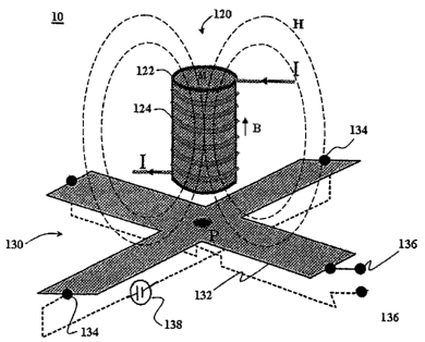
[0018] FIG. 1 shows a plan view of an exemplary embodiment of a memory cell in
accordance
with the present invention;
[0019] FIG. 2A shows a top view of an exemplary embodiment of a magnetic
switch in
accordance with the presentinvention;
[0020] FIGS. 2B-2C show a side view of the exemplary embodiment of the
magnetic switch
shown in FIG. 2A; and
[0021.] FIGS. 3A-3B show conceptual views of an exemplary embodiment of a
tunable magnetic
switch in accordance with the present invention.
[00221 FIG. 4 shows a graph illustrating the hysteresis loop for determining
the recoil
magnetization of the magnetic switch of the present invention.
[0023] FIGS. 5A-5H show various exemplary stages of fabrication for an
exemplary sensor in
accordance with the present invention.
[0024] FIG. 6 shows a scanning electron microscope (SEM) image of a fabricated
exemplary
sensor in accordance with the present invention.
[0025] FIGS. 7A-7D show various exemplary stages of fabrication for insulating
an exemplary
sensor in accordance with the present invention.
[0026] FIG. 8 shows an exemplary embodiment of an electroplating system in
accordance with
the present invention.
[0027] FIGS. 9A-9D show various exemplary stages of a fabrication process
(i.e., lift-off) for an
exemplary coil and magnet spot in accordance with the present invention.
[0028] FIG. 9E shows an SEM image of a fabricated exemplary sensor in
accordance with the
fabrication process of the present invention.
I-wA/2427 I 1 7.1 6
i.
~.
CA 02573406 2007-01-10
WO 2006/010258 PCT/CA2005/001167
[0029] FIGS. 10A-10D show various exemplary stages of fabrication for
depositing a magnetic
material on a magnet spot in accordance with the present invention.
[0030] FIG. 11 shows an SEM image of a fabricated magnetic switch in
accordance with the
present invention.
[0031] FIGS. 12A-12E show various exemplary stages of an altemative
fabrication process (i.e.,
direct etching) for an exemplary coil and magnet spot in accordance with the
present invention.
[0032] FIG. 12F shows an SEM image of a fabricated exemplary sensor in
accordance with the
alternate fabricating process of the present invention..
DETAILED DESCRIPTION OF THE PREFERRED EMBODIMENTS
[0033] Reference will now be made in detail to the preferred embodiments of
the present
invention, examples of which are illustrated in the accompanying drawings.
[0034] The present invention is directed to a magnetic memory device. In
particular, FIG. I
illustrates an exemplary embodiment of a memory cell of a magnetic memory
device according
to the present invention. Memory cell 10 according to an exemplary embodiment
of the present
invention includes a magnetic switch 120 and a sensor 130. The magnetic switch
120 includes a
magnetic component or material 122 and coil 124 to hold data. The sensor 130
includes a Hall
Effect sensor 132 and output terminals 136 connected to a voltage detector
(not shown) to detect
the stored data in magnetic switch 120.. ..
[0035] In particular, the magnetic switch 120 includes a magnetic component
122. The
magnetic component 122 may be a permanent magnet or a ferromagnetic material
(e.g., nickel or
nickel-iron magnet). A coaxial coil 124 (connected to a current source, not
shown) is disposed
about the magnetic component 122. The coaxial coil 124 is made of a conductive
material, such
I -wA/24271 17. l 7
CA 02573406 2007-01-10
WO 2006/010258 PCT/CA2005/001167
as the metal Ti/Au. However, any other suitable conductive material (e.g.,
Ti/Cu/Ti) may be
used without departing from the scope of the present invention. Although
magnetic component
122 is shown as having a generally cylindrical shape for purposes of
illustration, any suitable
sliape (e.g., square, rectangle, horseshoe) may be used without departing from
the scope of the
present invention. Furthermore, coaxial coil 124 is shown for purposes of
illustration as having
six (6) turns around magnetic component 122. However, any suitable number of
turns may be
used without departing from the scope of the present invention.
[0036] The Hall Effect sensor 132 includes a geometrically defined
semiconductor structure with
input terminals 134 connected to power supply 138 and output tenninals 136
positioned
perpendicularly to the direction of current flow. Although the Hall Effect
sensor 132 is shown as
having a "Greek cross" shape for purposes of illustration, any suitable shape
(e.g., rectangle)
may be used without departing from the scope of the present invention.
[0037] In general, the Hall Effect sensor responds to a physical quantity to
be sensed (i.e.,
magnetic induction) through an input interface and, in turn, outputs the
sensed signal to an output
interface that converts the electrical signal from the Hall Effect sensor into
a designated
indicator. In the present case, when the Hall Effect sensor 132 is subjected
to a magnetic field
(H) from a magnetic component 122, a potential difference appears across the
output terminals
136 in proportion to the field strength. When the Hall Effect sensor 132 is
subjected to an equal
and opposite magnetic field, an equal and opposite potential-di-fference-
appears across the same
output terminals 136. The Hall Effect sensor 132 thus acts as a sensor of both
the magnitude and
direction of an externally applied magnetic field.
[0038] In general, the shape and material used for magnetic switch 120
determines the strength
of magnetization (M) responsible for generating a magnetic field (H) around
sensor 130. The
I -wA/24271 17. t 8
CA 02573406 2007-01-10
WO 2006/010258 PCT/CA2005/001167
number of turns of the coil 124 around magnetic component 122, in conjunction
with the current
(D applied to the coil 124, determines the strength of the induced
magnetization (H) generated
around magnetic component 122 to set the direction and intensity of the
magnetization (M). The
dixection of the magnetization (M) of magnetic component 122 determines the
value of the
m.agnetic stored data (i.e., "0" or "1") in magnetic switch 120. The Hall
Effect sensor 132 is
characterized by voltage signal V}lail that is generated in response to the
magnetic field (H)
emanating from magnetic switch 120 detected at point P.
[0039) A current (1) (e.g., current pulse) is sent through the coil 124 in
such a way as to generate
a magnetic field H. The magnitude of the current is cuosen to be sufficient to
change (i.e.,
flip) the magnetization of the magnetic component 122. The magnetic field
generated by the
magnetic component 122 needs to be sufficient for the sensor 130 to detect it
at detection point
P. After detection, sensor 130 needs to generate a response (VHa ) greater
than an offset voltage
signal Voff. An offset voltage Vorf is the threshold that must be overcome
before any useful
signals are generated. More specifically, the magnetic field (H) generated by
the magnetization
(M) of magnetic switch 120 must be strong enough at point P to generate an
induced voltage in
sensor 130 greater than Voff before the stored data can be accurately
detected. A magnetic field
that generates a voltage signal less than the offset voltage cannot be
detected by the sensor 130 in
the present DC bias conditions.
[00401 FIG. 2A shows atop view of an.exemplary embodiment-of a magnetic
component -
surrounded by a coil. For purposes of illustration only, FIG. 2B shows a side
view of a magnetic
component 222 having an initial direction of magnetization (M) oriented
downward. FIG. 2C
shows that after a sufficiently high current (1) is sent through the coi1224,
the magnetic
component 222 retains an induced magnetization whose direction is oriented
upward. In.this
1-wn/24271 17.1 9
CA 02573406 2007-01-10
WO 2006/010258 PCT/CA2005/001167
case, the magnetic induction proxi.mate to the surface of the magnetic
component 222, at
detection point P, is the field generated by the magnetic component 222. This
field causes the
sensor.130 to generate a voltage signal that should have a magnitude greater
than the voltage
signal Vorr and a sign indicating the direction of magnetization (e.g., a
positive voltage for
"upward"). If an upward magnetization is designated as "1," then the sensor
130 detects the
stored data as being "1: "
[00411 To then attain a downward magnetization (i.e., "0"), a suitable current
(e.g., current pulse
in the opposite direction) is again sent through the coi1224 to generate a
magnetic field -H;j
(i.e., with the opposite orientation than H,o;j) sufficient to change (i.e.,
flip) the magnetization' of
the magnetic component 222. After the pulse, the magnetic component 222
retains a
magnetization that may have smaller magnitude or whose direction is oriented
downward. In
this case, the magnetic field at detection point P is the magnetic field
generated by the magnetic
component 222. The detected induction at point P causes the sensor 130 to
generate a voltage
signal that has a smaller magnitude or opposite sign indicating the direction
of magnetization
(e.g., a negative voltage for "downward"). If a downward or smaller
magnetization is designated
as "0," then the sensor 130 detects the stored data as being "0."
[00421 In another embodiment of the invention, a tunable magnetic switch
according to the
present invention ensures operational reliability of the fabricated magnetic
memory device. In
particular, the offset voltage threshold. Vaff as discussed above may-be
larger than expected: The
offset of the sensor are caused by such things as non-uniformity of the device
and misalignments
that occur during fabrication. The magnetic induction (B) generated by the
magnetization (M) of
magnetic switch 120 must be strong enough at point P to generate an induced
voltage in sensor
130 before the stored data can be accurately detected. Once the memory device
containing an
I-wA/2427 117.1 . 10
CA 02573406 2007-01-10
WO 2006/010258 PCT/CA2005/001167
array of memory cells 10 is fabricated, the internal components cannot be
rearranged to reduce
the operating offset threshold Voff. To address this problem, a tunable
magnetic switch according
to the present invention ensures operational reliability of the fabricated
magnetic memory device
by allowing the detected magnetic field to be tuned after the fabrication
process, as presented
below.
[0043] FIGS. 3A and 3B illustrate an exemplary embodiment of a tunable
magnetic switch
according to the present invention. For purposes of illustration, FIG. 3A
shows a tunable
magnetic switch 320 including two magnetic component 322 and 330. The magnetic
component
322 is coupled to a three (3) turn coil. However, any suitable number of turns
may be used
without departing from the scope of the present invention. The magnetic
component 322 may be
a soft cylindrical bar magnet made of ferromagnetic material (e.g., nickel-
iron magnet). The
magnetic component 330 may be a hard permanent magnet made of ferromagnetic
material (e.g.,
nickel, cobalt, and other related alloy magnets). Although magnetic components
322 and 330 are
shown as having a particular shape for purposes of illustration, any suitable
shape may be used
without departing from the scope of the present invention.
[0044] As shown in FIG. 3B (i.e., side view), magnetic switch 320 is exposed
to an external
magnetic bias field Hbi. provided by the magnetic component 330. Once a
biasing field Hbi,,s is
established over magnetic switch 320, a current (I) (e.g., current pulse) is
sent through the coil in
such a way as to generate a magnetic field (H). having the samedirection and
orientation as the -
bias field H b;~,,. The magnitude of the current pulse is chosen to be
sufficient to drive magnetic
component 322 to its saturation magnetization value.
[0045) For purposes of illustration only, the direction of magnetization (M)
of the magnetic
component 322 is shown as initially being oriented downward, in the same
direction as the
I-wnn4271i7.- 11 i
[
CA 02573406 2007-01-10
WO 2006/010258 PCT/CA2005/001167
constant bias field Hbiu. After the current (I) is sent through the coil 324,
the magnetic
component 322 retains a high magnetization. In this case, the magnetic f e1d
proximate to the
starface of the magnetic component 322, at detection point P, is the
combination of the bias field
He,i~ and the field generated by the magnetic component 322. This combined
field results in a
very high magnetization state, generating a voltage signal much greater than
the offset voltage
Vprr. Hence, the sensor 130 easily detects the stored data as being "1," for
example, assuming
that the downward direction of magnetization (M) is designated as a high state
(i.e., "1 ").
[0046] To attain a low state (i.e., "0"), a suitable current (I) (i.e.,
current pulse) is sent through
the coil 324 to generate a magnetic field -H,o;, in the opposite direction to
the bias field Hy;,,,
sufficient to generate a total magnetic field (i.e., H,,ii + Hbias) that
demagnetizes the magnetic
cornponent 322. After the current is sent through the coi1324, the
magnetization (M) will recoil
following the recoil line, explained further below in reference to FIG. 4,
providing a magnetic
component 322 with a very low magnetization. If the current is strong enough,
the
magnetization (M) may even be oriented in the opposite direction. In this
case, the magnetic
field at detection point P will be that of the bias field Hbial combined with
the magnetic field
generated by the magnetic component 322, which is either very low or in the
opposite direction
of the bias field Hb;as. In either instance, the total magnetic induction at
point P will be
significantly lower than that corresponding to the high level case, non-
existent, or even in the
opposite direction. Accordingly,a definitive low level state (i:e:, "a") may
be detected-by the
sensor 130.
[00471 The switching behaviour shown schematically in FIGS. 3A and 3B may be
explained
using the hysteresis loops of the magnetic component 322 as shown in FIG. 4.
First, the
intersection of the induction load line and the induction hysteresis loop
define a point "a" with
t -wrv242711 7.1 12
CA 02573406 2007-01-10
WO 2006/010258 PCT/CA2005/001167
irnduction B1. Point "a" may then be used to determine the corresponding point
"b" on the
rnagnetization loop. The magnetization load line can then be drawn. This load
line is then
translated by Hc~;l along the magnetic field axis to establish a new
intersection at point "e" on the
magnetization hysteresis loop. The corresponding point 'f' on the induction
loop may then be
established. After H,oil is removed (i.e., current pulse is removed), the
magnetic component 322
will recoil. Using point "fl' and the recoil permeability, the recoil line can
then be drawn.
Finally, the intersection point "g" of the recoil line and the magnetization
load, line can be
determined, providing the induction B2. Induction B2 is then set as the
induced magnetization
(M) that is stored in magnetic component 322 once the current (I) is removed
in establishing the
low state (i.e., "0").
[00481 The fabrication process will now be explained with reference to FIGS. 5-
10. The
fabrication process of the memory cell 10 (as shown in FIG. 1) may be divided
into 2 parts: (1)
fabrication of the sensor 130, and (2) fabrication of the magnetic switch 120.
For the tunable
magnetic switch, an additional process for fabricating the bias magnetic is
included.
[00491 The Hall Effect sensor 132 is fabricated with high mobility materials,
such as III-V
materials (i.e., compounds formed from groups III and V elements of the
periodic table). III-IV
materials include, but are not limited to, GaAs, InAs, InSb, and related two-
dimensional electron
gas (2DEG) structures. A 2DEG structure based on a GaAs/AIGaAs hetero-
structure may be
formed at the hetero junction.interface of a modulation-doped hetero=structure
between a doped
wide band-gap AlGaAs material (i.e., barrier) and an undoped narrow band-gap
GaAs material
(i.e., well). Ionized carriers (from the dopant) transfer into the well,
forming the 2DEG. These
carriers are spatially separated from their ionized parent impurities and,
therefore, allow for high
carrier mobility and a large Hall Effect. Although only III-IV materials are
discussed here, other
I-wrV2427117.t 13
CA 02573406 2007-01-10
WO 2006/010258 PCT/CA2005/001167
materials (e.g., silicon) may be used to fabricate the Hall Effect sensor 132.
[0050] FIGS. 5A-5D illustrate the various fabrication stages of the Hall
Effect sensor 132 in
accordance with an exemplary embodiment of the present invention. A suitable
wafer 538, such
as a semi-insulating GaAs wafer with a thin n-type active GaAs film 539 (about
0.5-0.6 m), is
used. A layer of resist 540 (e.g., 950K PMMA 4%) is spun onto the wafer 538.
The following
spin conditions may be used: spin rate = about 4000 rpm (thickness=0.5-2 m);
bake
temperature =160 C; soft-bake time = 7 minute; exposure energy = 25kV;
exposure dose = 150
C/cm2; developer = MBIK/IPA mixture (1:3); development time = 25 seconds. The
resist layer
540 is patterned through EBL (i.e., electron beam lithography); however, any
suitable patterning
technique (e.g., photolithography with standard AZ resist type) may be used. A
mesa etch
process is then carried outfor insulating the sensor. The etch process
involves wet etching with,
for example, a standard H202/H3P04/H20 solution.
[00511 Following the etching process, the input terminals 134 and output
terminals 136 (FIG. 1)
are deposited through a lift-off process. As shown in FIGS. 5E-5H, the lift-
off process involves
spinning a layer 542 made of double layer copolymer/PMMA (at 4000 rmp). The
lift-off profile
(i.e., under-etching) provided by the difference of sensitivity between the
copolymer and the
PMMA during the development process and after the exposition to an electron
beam. A contact
layer 544 of suitable material, such as gold-germanium (AuGe), is evaporated
onto the wafer 538
to a thickness of about 400 nm to form ohmic contacts 134 and 136-to be used
as input and
output terminals of sensor 130. A layer of nickel may be added to the AuGe
layer 544 to
improve contact performance.
[00521 Following the evaporation step, the lift-off process is completed by
placing the wafer 538
in acetone in order to remove any unnecessary portions of the AuGe layer 544.
After appropriate
t-WA/24271i7.t 14
CA 02573406 2007-01-10
WO 2006/010258 PCT/CA2005/001167
cleaning, the contacts (i.e., AuGe layer 544) undergo rapid thermal annealing
(RTA). The
annealing is carried out at about 340 C for about 40 seconds in an RTA chamber
filled in
nitrogen (N2) flow. The lift-off process is completed by placing the wafer 538
in acetone in
order to remove any unnecessary portions of the AuGe layer 544. FIG. 6
illustrates the GaAs
Greek cross Hall Effect sensor with AuGe contacts. Also shown are alignment
marks 546
included in the pattern.
[0053] Although the resist PMMA 4% is used in the example above, any suitable
resist, such as
PMMA 2% may be used. Moreover, HMDS, an adhesion promoter, may be used as
needed.
When using P1VI!vIA 2% as the resist, the following lithography processing
parameters may be
used: PMMA (2%); exposure energy = 15kV; exposure dose = 150 C/cmZ; developer
=
MBIK/IPA mixture (1:3); development time = 25 seconds.
[0054] Once the Hall Effect sensor 132 is fabricated, an insulating layer 748
is spun onto the
Hall Effect sensor 532. The insulating layer 748 is made of a suitable
material, such as a
dielectric polyimide, which may be processed as typical resists (i.e., spun
onto a wafer and baked
in an oven or on a hot plate). An example of a dielectric polyimide is HD
Microsystem's P12545
(an inter-metallic, high-temperature polyimide used in various microelectronic
applications). It
has a high glass transition temperature (i.e., about 400 C) and may be
patterned with positive
resist. Moreover, the cured film is ductile and flexible with a low CTE, and
is resistant to
com.mon wet and dry processing chemicals. Other suitable.materials include
silicon oxide and
silicon nitride, which may be deposited through Plasma Enhanced Chemical Vapor
Deposition
(PECVD) at low temperatures.
[0055] For illustrative purposes only, FIGS. 7A-7D show an insulating layer
748 of P12545 spun
onto the Hall Effect sensor 532 at a rate of about 6000 rpm and then soft-
baked on a hot plate.
1-WA/2427117.1 15
CA 02573406 2007-01-10
WO 2006/010258 PCT/CA2005/001167
The temperature is ramped from 25 C to 170 C at 240 C/li. Once an oven or hot
plate
te-inperature of 170 C is reached, the temperature is kept constant for 9
minutes (i.e., soak
period). After the soak period, the hot plate cools down to room temperature
by natural
co:nvection. When the insulating layer 748 is baked at an oven or hot plate
temperature of about
140 C or 170 C, it develops a good chemical resistance to boiling acetone,
which is later used to
rer~nove a resist layer.
[0056] Once the insulating layer 748 is deposited, a positive resist layer 750
(e.g., PMMA 4% or
AZ5206) is spun onto the insulating layer 748. For purposes of explanation,
PMMA 4% is used.
The resist layer 750 is then baked in an oven or hot plate at a temperature of
160 C for two (2)
minutes, with a ramp rate of 6 C/minute and a soak period of 6 minutes. A
baking temperature
of 160 C is the minimum safe bake temperature for PMMA (e.g., PMMA baked at
120 C may
exhibit some adhesion failure).
[00571 Then, the wafer is placed into an EBL chamber, where it is exposed to
25 kV of electron
beam. The resist layer 750 is patterned in such a way as to make openings over
the Hall Effect
sensor's ohmic contacts and alignment marks (if any). For a pattern of the
size 9 X 10 mZ, an
appropriate dose may be in the range of 165 - 182 C/cm2; for a pattern of the
size 17 X 17 m2,
an appropriate dose may be in the range of 149 - 163 C/cm2; and.for a pattem
of the size 100 X
112 gmz, an appropriate dose may be in the range of 132 - 145 C/cm2.
[0058] After exposure, the resist layer 750 is developed-in a suitable
solution, such as -
MIBK/alcohol (1:3), for a suitable amount of time (e.g., about 40 - 55
seconds). The wafer is
then rinsed in alcohol and de-ionized water. Once the wafer is cleaned, a
diluted PPD450 (1:5)
solution is used for etching the insulating layer for a suitable amount of
time (e.g., about 6-14
minutes or even longer). The degrees of dilution and agitation and the
development and etching
I -wA/24271 t 7.1 16
CA 02573406 2007-01-10
WO 2006/010258 PCT/CA2005/001167
times may be changed as needed. Boiling acetone is used to remove the resist
layer 750 (i.e.,
PMMA). Finally, to complete fabrication of the insulating layer 748, the
insulating layer 748 is
hard-baked at about 200 C using a temperature ramp as described above. The
insulating layer
may be hard-baked at a temperature as high as 400 C. However, such high
temperature may
create unwanted diffusion in the Hall Effect sensor.
[0059] Once the sensor 130 is fabricated, the magnetic switch 120 is
fabricated over the
insulating layer 748. The general approach to fabricating the magnetic switch
120 is to first
fabricate the coil 124, and then to fabricate the magnetic component 122.
Traditional methods
fnr fabricating :nagnetic materials (e.g., Alnico and Martensitic steel)
involve synthesis rouies
that include, for example, melting different components, casting, and high
temperature (typically,
above 800 C) thermal processing (e.g., quenching). Other synthesis routes
include sintering and
extrusion. These methods are incompatible with micro-technology or wafer-scale
processing due
to the extremely small sizes of the components.
[0060] Electroplating, on the other hand, allows for relatively good
definition of element shapes
with fewer defects on element walls. It is also an inexpensive and relatively
simple process to
implement. Three-electrode systems can be used to monitor the stoichiometry of
deposited
alloys.
(00611 Electroplating will be used in explaining the fabrication process of
the magnetic switch
120; however, any suitable synthesis routemay be utilized. As shown in FIG. 8,
an
electroplating system 800 includes an electroplating.ce11810, a computer 820,
and a computer-
driven potentiostat/galvanostat 830. The computer 820 is connected to
electroplating cell 810
through the potentiostat/galvanostat 830 to control the electroplating
process. The
potentiostat/galvanostat 830 can function as either a potentiostat or a
galvanostat.
t=wAl2427117.1 17
CA 02573406 2007-01-10
WO 2006/010258 PCT/CA2005/001167
[0062] First, the coil and a magnet spot or area within the coil where the
magnetic component is
to be deposited are formed over the sensor 130. A first exemplary process for
forming the coil
and the magnet spot involves a titanium/gold lift-off process. FIGS. 9A-9D
illustrate various
stages of fabrication of according to the gold lift-off process according to
the present invention.
[0063] The insulating layer'748 (from FIG. 7D) is first covered with a double
resist layer 954
(e. g., copolymer/PMMA). For that, a layer of the copolymer E11 is first spun
onto the wafer.
Then, the copolymer layer is baked at 160 C for 5 minutes on a hot plate with
a temperature
rarnp as described above. The hot plate is left to cool to room temperature by
natural convection.
Then, a layer of PMMA 4% in anisole is spun onto the wafer and baked at 160 C
for 5 minutes
using the defined temperature ramp. The hot plate again is left to cool to
room temperature by
natural convection.
[0064] The wafer is placed into the EBL chamber, where the double resist layer
954 is exposed
to an electron beam so as to pattern the coil 924 and magnet spot 923, with an
exposure of 25kV
and various doses: for a fine coil pattern, an appropriate dose is 150 C/em2;
for the magnet spot,
an appropriate dose is 120 C/cm2; for alignment marks (if any), an
appropriate dose is 195
C/cm2. The alignment marks can be included in the pattern to aid in the
location of the magnet
spot. The double resist layer 954 is then developed into a suitable solution,
such as
MIBK/alcohol, for about twenty (20) seconds.
-[0065] After the patterning step, the wafer is placed into an electron bearim
evaporator, where
titanium layer 952a and gold layer 952b of 25 nm and 150 nm, respectively, are
deposited onto
the patterns to form the Ti/Au layer 952. Titanium layer 952a is used as an
adhesion layer.
Finally, the wafer is removed from the evaporator and dipped into acetone for
about one hour to
remove the double resist layer 954 and any unwanted Ti/Au layers 952. As shown
in FIG. 9F,
1-WA/2427117.1 18
CA 02573406 2007-01-10
WO 2006/010258 PCT/CA2005/001167
the coil 924 and magnet spot 923 are obtained. In this exemplary embodiment,
only a single turn
coil 924 is used. However, different number of turns may be used as
appropriate without
departing from the scope of the invention.
[00661 After depositing the coi1924, magnet spot 923, and alignment marks (not
shown), the
magnetic component 122 is electroplated onto the magnet spot 923 through a
mould that
provides the shape and dimensions of the magnetic component 122. As shown in
FIGS. l0A-
lOC, to fabricate such mould, EBL is used to pattern a thick (e.g., about 10
m) layer 1058 of
resist (e.g., AZ4620) onto the coi1924, magnet spot 923, and alignment marks
(not shown). The
resist layer 1058 is baked at about 95 C for about 4 minutes. Then, the resist
layer 1058 is
placed into a chamber for EBL, where the areas where the alignment marks are
located are
exposed to an electron beam. Following this exposure, the resist layer 1058 is
developed in a
suitable solution, such as PPD450, and removed from the areas where the
alignment marks are
located. The wafer is cleaned with de-ionized water and blown dry with N2.
Then, using EBL
(and the alignment marks as a guide), the magnet spot 923 is patterned and the
resist layer 1058
is developed for a second time in order to obtain a well 1060. Well 1060
functions as a container
into which a magnetic material is electroplated to form the magnetic
component.
[00671 The wafer with the resist template is then placed into an
electroplating cell 810 (FIG. 8),
where pulsed deposition (with, e.g., a 2% duty cycle, where t T = 1 ms; taff =
49 ms; and the peak
current is about 1.4 mA) is used to deposit magnetic material 1070-(e.g.,
nickel-or nickel-iron)
onto the resist template forming the well on the magnetic spot to thereby form
an array of
magnetic components 122: Pure materials are generally easier to deposit.
However, alloys may
also be used. Examples of materials that can be deposited include cobalt,
iron, nickel, nickel-
iron (NiFe), and cobalt-nickel-iron (CoNiFe). Different catalysts may be used
to increase the
1-WA/2427 1 1 7.1 19
CA 02573406 2007-01-10
WO 2006/010258 PCT/CA2005/001167
coercivity of these materials if needed.
[0,068] For illustrative purposes, a nickel chloride based solution with two
additives, namely
sa~ccharin (which acts as a strain relief agent) and sodium lauryl sulfate
(which acts as a
surfactant), is deposited into the well 1060. A current, such as a DC current,
is used to fabricate
the magnet component. For an even smaller, higher aspect ratio structure,
pulsed electro-
deposition (with, e.g., a 2% duty cycle) may be used to deposit magnetic
material (e.g., nickel or
nickel-iron) onto the resist template to form an array of magnetic component
122. The
electroplating conditions are controlled by the computer-driven
potentiostat/galvanostat 830.
Although the shape of the magr,et is cylindrical, any shape (e.g., rectangle,
square) may be
developed using the above technique. After electro-deposition, the mould
(i.e., thick resist layer
1058) is removed using a suitable solution, such as acetone. FIG. 11 shows a
magnetic switch
developed using the above process.
[0069] Once magnetic switch 120 has been completed, further processing steps
may be
implemented to fabricate the tunable magnetic switch as shown in FIGS. 3A and
3B. For
instance, an insulating layer 748 is deposited on the top of the magnetic
switch 120. Then, a
hard permanent magnet, for example, is added on the top of the structure by
hybrid integration of
prefabricated micro-magnets or by electroplating hard ferromagnetic material,
such as cobalt or
selected alloys, bn the insulating layer 748.
[0070] Although EBL is used as_ the exemplary method for fabricating the
mould, any suitable
method, such as photolithography, may be used. For example, when using
photolithography, the
mould is formed by exposing the resist layer (i.e., AZ4620) to UV light
through a suitable
prefabricated hard mask.
[0071] Another approach to fabricating the coil 924 and magnet spot 923
involves etching
1-wn/2a27 t t 7.1 20
{
CA 02573406 2007-01-10
WO 2006/010258 PCT/CA2005/001167
directly the seed layer 952 so as to obtain the coil 924 and the magnet spot
923 in the same
process step as shown in FIG. 12A-12E. A key concept is to use the seed layer
925 for the
growth of the magnetic component 122 and, at the same time, for making the
coil 924. First, the
wafer carrying the seed layer 952 (i.e., Ti layer 952a, Cu layer 952b, Ti
layer 952c) is patterned
through, for example, EBL. This patterning step can incorporate the use of a
positive resist layer
1210 and wet etching. Again, the pattern includes a single loop coil around a
central metallic
spot, with a metallic path linking it electrically to a common electrode used
for electroplating.
However, any suitable number of turns may be used.
[0072] The wafer is dried by baking it on a hot plate for about 30 minutes at
about 150 C. A
layer of resist 1210 (e.g., AZ5206E) is spun onto the wafer. The resist layer
1210 is soft-baked,
starting from about 95 C and then lowered to about 80 C, the change in
temperature time being
about six (6) to seven (7) minutes. The resist layer 1210 is then exposed
(e.g., exposure energy =
about 10 kV; dose = about 6 C/cmZ). After exposure, the wafer is developed in
a suitable
solution, such as PPD450. The wafer is then cleaned with de-ionized water.
After the cleaning
step, the wafer is hard-baked for about 10 minutes at about 125 C. The
titanium (Ti) and copper
(Cu) layers are etched with suitable solutions. For example, the Ti layers
952a and 952c may be
etched with a highly diluted HF/HNO3/H2O solution, while the copper layer 952b
may be etched
with a HCI/H202/H20 solution. The wafer is then cleaned to remove resist 1210.
The cleaning
step can include, for example, boiling acetone, boiling alcohol, and de-
ionized water rinsing.
Once the coil 924 and magnet spot 923 have been etched directly into the seed
layer 952, the
wafer undergoes the process for creating the mould for electroplating the
magnetic component as
described above.
[0073] The magnetic memory device according to the present invention was
described in relation
i-wnn4271i7.1 21
CA 02573406 2007-01-10
WO 2006/010258 PCT/CA2005/001167
to a magnetic switch over a Hall Effect sensor. In particular, the advantages
of a magnetic
component that can retain a magnetic field without any power supplied thereto
and a simple
sensor for reading the stored magnetic field provides a non-volatile memory
device that
consumes very little power for operation compared to the electric-based memory
devices
currently in use.
[0074] Additionally, the tunable magnetic switch according to the present
invention was
described. The advantages of the tunable magnetic switch according to the
present invention are
numerous. First, because the magnetic component retains the induced
magnetization (M) from
the induction coil, the tunable magnetic switch according to the present
invention can function as
a switch with non-volatile memory.
[0075] Second, the tunable magnetic switch according to the present invention
provides a
sufficiently high field for the Hall Effect sensor so as to partially or even
completely compensate
for the sensor offset. In the case of the former, the tunability of the
magnetic switch according to
the present invention, i.e., the bias field may be adjusted relative to the
sensor offset, allows for a
larger tolerance of fabrication constraints, makes fabrication much easier,
and increases
reliability of the devices. This is a considerable asset for miniaturization
as the sensor offset
increases as size of the devices are scaled downward.
[0076] Yet another significant advantage of this approach is that the tunable
magnetic switch
according to the present invention.allows.usage of low aspect ratio magnets,
which are much
easie.r to fabricate, since the bias field compensates for the demagnetization
of the magnetic
component of the memory cell. The tunable magnetic switch according to the
present invention
was described in relation to a magnetic memory device using Hall Effect
sensors. However, the
tunable magnetic switch according to the present invention may be applied with
other magnetic
1-w1v242? 117. t 22
CA 02573406 2007-01-10
WO 2006/010258 PCT/CA2005/001167
memory devices as the bias magnetic field used for tuning the magnetic switch
may be applied to
any magnetic component and sensor configuration.
[0077) The magnetic memory device according to the present invention has
various applications
including, but not limited to, radio frequency identification tags (RFIDs),
personal digital
assistants (PDAs), cellular phones, and other computing devices.
[00781 It will be apparent to those skilled in the art that various
modifications and variations can
be made in the tunable magnetic switch of the present invention without
departing f rom the spirit
or scope of the invention. Thus, it is intended that the present invention
cover the modifications
and variations of this invention provided they come within the scope of the
appended claims and
their equivalents.
t-wn/24271 17.t 23