Note: Descriptions are shown in the official language in which they were submitted.
CA 02573707 2007-01-11
PHASE-COHERENT SICiNAL GENERATOR
FIELD OF THE DISCLOSUR.E
[001] The present disclosure generally relates to the field of frequency
synthesizers.
More specifically, the present disclosure relates to a method and apparatus
for generating
phase-coherent broadband tunable frequencies.
BACKGROUND
[002) Synthesizers are designed and used to generate signals in a broad
spectrum of
frequencies while enabling rapid switching between frequencies selected within
that
spectrum. Traditional analog synthesizers have long been replaced by digital
synthesizers, which are generically named Direct Digital Synthesizers (DDS).
Modem
DDS are increasingly used due to low cost, ease of frequency control, high
switching
speed from one frequency to another and the ability to precisely tune the DDS
to any
selected frequency within a very wide frequency spectrum. There are available
devices
that can, for example, generate signals with frequencies in an operational
band of 40
MHz and with resolution of 0.1 Hz (< 0.01 Parts Per Million (PPM)). Today, DDS
frequency generators are cost effective and competitive; they introduce high
performance
and can be functionally integrated in small sized packages. The integration of
high-speed
high performance digital to analog converter (DAC) and DDS architecture onto a
single
electronic Integrated Circuit (IC) chip, thus forming what is commonly known
as a
Complete-DDS solution, enables to 'compiess' a wide range of applications into
economical and densely packaged systems and modules.
-1-
CA 02573707 2007-01-11
[003] Thanks to its many advantages, DDSs are more and more used by electronic
circuits architects and designers, especially where agile frequency shift(s)
or changes are
required.. Other signal generation techniques (other than DDS techniques)
typically use
some sort of an oscillator to generate an initial signal that is further
manipulated or
controlled by a frequency syntliesizer. Since, by nature, oscillators run
freely, there is no
control over the phase of the signals that they generate. Therefore, if, at a
certain instant,
it is desired to switch the frequency of an analog synthesizer= from one
frequency to
another, an unwanted phase change will occur often. DDS-based solutions are
unique in
this respect, as DDS circuits are digitally deterministic in their structure.
That is, instead
of using an oscillator to generate a signal with un-controllable phase, the
DDS-based
circuits synthesize new output signals to obtain some control over the
signal's phase.
Several circuit designs for frequency generation and control may be adopted by
a circuit
designer, ranging from Phased Locked Loops (PLL) based tecluiiques to dynamic
programming of digital to analog converter (DAC) based systems.
[004] The basic principles of DDS have substantially remained the same for
years. A
DDS signal generator operates by storing in a memory, in a digital format,
selected
points representative of a complete cycle of a waveform, and recalling stored
points from
the memory, in a cyclic manner (to replicate a single cycle), to generate the
wanted
waveform. The rate in which the synthesizer completes a complete cycle of the
waveform governs the frequency of the generated wave: the faster the
synthesizer
completes a cycle, the higher the frequency.
-2-
CA 02573707 2007-01-11
[005] A conventional DDS architecture is typically based on a phase
accumulator, a
mapping device and a DAC. A phase accumulator is an arithmetic device that
discretely
performs the mathematical integration Sn=Sn-1 + d, where 'Sn' is a new phase
value,
'Sn-1' is a phase value preceding Sn and 'd' is a phase increment, This means
that during
a discrete integration, a new (next) phase (Sn), may be created by taking the
last
calculated phase value (Sn-1), and adding to it a phase increment (d). Two
basic DDS
phase accumulator structures were developed and may co-exist in the market.
One DDS
phase accumulator directly manipulates binary data and the other DDS phase
accumulator operates with decimal values, by accumulating data in a binary
coded
decimal (BCD) format.
[006] The DDS memory unit (mapping device) performs the non-linear
transformation,
or conversion, of'each value of x=w*t (the phase argument, where w = 2)r *, f
and 'fis
the frequency) into a corresponding value Sin(x). This function is usually
implemented
using a lookup table (LUT) where each x value has a corresponding Sin(x)
value. x and
Sin(x) values are often stored in ROM/RAM memory components.
[007] Applications that exploit DDS units roughly fall into two categories.
The first
category includes communication applications that use DDS unit(s) as building
block(s)
for of providing agile (immediate response) frequency sources. The second
category
includes many applications in the industrial and biomedical fields, where a
DDS is
implemented as a programmable waveform generator module, as it permits simple
adjustments of frequencies in real time, a feature highly required in may of
such
applications. A DDS frequency generator is digitally programmable, which
allows the
-3-
CA 02573707 2007-01-11
phase of the signal, and in the general the signal's waveform, to be easily
adjusted
without needing to change hardware components, as opposed to traditional
analog
programmed waveform generators.
[008] DDS structure and related performance may be adapted to obtain a
required
signal phase. Generation of' a typical signal by a DDS frequency generator
usuaily
involves the generation of successive sinusoidal signals, where two adjacent
sinusoidal
signals have different frequencies (f) for a designated duration (AT). While
DDS
frequency generators may function well in some applications in terms of phase
properties, additional efforts are still required to further improve aspects
of the signal's
phase when DDS frequency generators are used in certain applications and, in
particular
in Radar (Radio Detection and Ranging) simulations.
[009] For Radar pulse synthesis, for example, it is necessary to comply with
quite a
wide frequency operational band and very high degree of spectral purity to
support
stringent requirements associated with the correct dynamics of a Radar system.
The DDS
frequency generator has to comply with stringent specifications which means,
in general,
that the DDS frequency generator has to output a signal with very accurate
frequency and
amplitude modulation, for facilitating accurate intra-pulse modulation. Modern
Radar
simulation applications usually require phase coherency, wliich implies that
it is also
required to precisely control the phase of the signal output by the DDS
frequency
generator_
-4-
CA 02573707 2007-01-11
[0010] For a synthesizer to be phase coherent it is required that when the
frequency of
the DDS signal shifts from one value (for example fl) to another (for example
f2) and
then back to the original value (fl), the phase of the DDS signal, when its
frequency
changes back from f2 to f 1, should retain the phase value of the original
frequency (f 1) as
if'there the frequency changes (from fl to f2 and back to fl ) never occurred.
[0011] The concept of phase-coherent waveforms and continuous phase waveforms
can
now be introduced. The phase of a low frequency signal changes relatively
slowly,
whereas the phase of a high-frequency signal changes relatively fast. These
two reference
signals may oscillate without any interruption and shall be used as a
reference for the
sake of explanation. A third signal may start as a high-frequency signal and
it may have
the same phase as the high-frequency reference signal. After some time the
signal's
frequency may switch from high frequency to low frequency. At this time, the
signal has
the same phase as the reference low-frequency signal. After some more time
lapses, the
signal frequency may resume its high frequency. Again, the signal has the same
phase as
the high-frequency reference signal. This type of waveform is called a phase-
coherent
waveform since this type of waveform always has the phase of the reference
signals
involved. As a result of this behavior of the phase, there might be a
phase,jumps during
transitions from one frequency to another, which results in non-continuous
phase.
[0012] The frequency of a fourth signal may switch from high value to low
value and
resume the high value. However, the fourth signal may have a smooth
(continues) phase.
In a signal whose phase is continuous, changing the signal's frequency from
one value to
another results in the signal's phase differing from the phase value of'any of
the reference
-5-
CA 02573707 2007-01-11
signals involved. This kind of waveform is called in the art a'continuous-
phase
waveform'. This type of phase behavior is very problematic to many
applications such as
radar applications. From the fourth signal characteristics it can be
understood that, when
jumping between several frequencies, each time the signal resumes one of its
the several
frequencies, it has a phase that is different than the phase of the resumed
frequency.
[0013] There is another significant requirement, and therefore a corresponding
design
parameter, that must be taken care of by a system designer, in order to
achieve a better
performance, as required by applications such as Radar simulation systems.
Obtaining
both a low dwell time and, at the same time, good frequency resolution, is
complicated.
A dwell time is defined as the time length between the starting instants of
two signals
with different frequency, and it is reversely proportional to the frequency
hopping rate.
[0014] In addition, output signals of a high quality system require many bits
to define
both w*t and Sin(wt). Therefore, a large memory space is highly required to
support the
storage needs of the digitized data stored in a lookup table which is required
for
reconstructing the w*t and Sin(wt) functions. Since retrieving data from a
memory
device is the slowest process in such a signal processing chain and huge
memories
consume a lot of physical space, a new approach had to be found.
[0015] Commercially available DDS frequency generators are based on an
architecture
that typically includes a Phase Accumulator (hereinafter called an
accumulator). The
accumulator's output value is periodically increased by a constant step size
(on the
0 = 360' cycle). The larger the step size the higher the signal's frequency .
The
-6-
CA 02573707 2007-01-11
accumulator's value is used to generate a Phase Word. The Phase Word is fed to
a Sin(x)
Look Up Table (LUT). The Sin(x) LUT converts the phase word into an amplitude
word
and the LUT's output is fed to a DAC to generate a corresponding analog
signal. When a
low frequency generation is required, the Accumulator's output is increased in
relatively
small steps. When a higher frequency generation is required, the Accumulator's
output is
increased in larger steps. Therefore, in such DDS devices, the value of the
DDS's output
frequency can be controlled (changed) by varying the Accuniulator's output
step size.
[0016] Using the above-described phase accumulator mechanism results in a
signal
having a continuous phase, which means that whenever a frequency change
occurs, the
phase of the signal continues from the phase value stored in the Phase
Aecumulator. As
is explained earlier, continuous phase is an unwanted quality in some
applications such
as in Radar related applications. It is tlierefore clear that conventional DDS
devices,
which utilize phase accumulators, are inherently non-phase coherent, though
for these
types of applications phase coherency is a must_
[0017] Several methods for overcoming the non-coherent behavior of the phase
accumulator based DDS circuits were previously suggested and implemented in
operational circuits. Some of these methods require that the phase accumulator
be reset at
a pre-determined rate. This approach may work only if and as long as the dwell
time for
each frequency and frequency jump(s) aligns witli the system reset cycle time.
This
means that the performance of DDS frequency generators in such a configuration
is
limited to low hopping rate at specified times. Other methods are based on
calculating
the required phase for a new given frequency and then modifying the phase
accumulator
-7-
CA 02573707 2007-01-11
value to comply with the calculated required phase value. This approach is
also limiting
the frequency hopping rate of the device, because the new required phase-value
calculation time, together with the associated phase modification cycle time,
require a
comparatively long dwell time, that, again, limits the frequency hopping rate,
or
switching speed, of the related DDS.
[0018) Architecture, called by its author Multiplying Digital Synthesizer
(MDS), which
enables the generation of phase-coherent signals useful, for example, in Radar
and
similar application, was previously introduced. The MDS architecture is not
using a
phase-accumulator. Instead, the MDS architecture uses a phase-counter that is
connected
to a Sine(x) sampled LUT which is stored in a memory module. The main drawback
of
this architecture is that, for small frequency steps (such as 1Hz, which is
commonly used
in many applications), the size of the LUT is very large (it typically
includes 100 million
entries, and, sometimes, even more). Such LLJTs are impractical for commercial
use due
to the costs and sizes of the memory required, and because of the relatively
slow memory
access time associated with the size of LUT.
GLOSSARY
[0019] PLL (Phased locked loop)- An electronic circuit that typically consists
of a
phase/frequency detector (PFD), low pass filter (LPF), and voltage-controlled
oscillator
(VCO). PLLs generate a waveform that has phase coherence to a reference
waveform by
using a feedback loop to control the phase locking process. PLLs are
relatively slow by
nature, and they do not support or enable fast frequency hopping.
-8-
CA 02573707 2007-01-11
[0020] DAC (Digital to Analog Converter) - A device or a circuit that converts
a digital
representation of a certain parameter (for example voltage or current) value
into an
analog level presentation of that value.
[0021] LAN -(Local Area Network), a localized data communication network
supporting data communication among a plurality of computer terminals and also
supporting the sharing of common network resources, such a memory and input
and
output (UO) devices.
[0022] Phase Accumulator - An electronic arithmetic circuit used to accumulate
and
store the value of the synthesizer signal's phase.
[0023] Sin(x) Look Up Table (LUT) - A lookup table for storing, in a digital
format, a
set of discrete values of a sampled sinusoidal signal or a set of values
calculated using the
Sin(x) function. The function is sainpled for a discrete number of N values,
interspaced
by a predefined delta X (dX ) incremental number,
[0024] Most Significant (n) Bits (MSBs)- The most significant n number of
bits, taken
from left to right in a binary representation of a number.
[0025] A multiplier - A device or an electronic circuit that takes in the
value of at least
two inputs and generates a signal at its output that is the result of the
inputs values
multiplication by each other.
-9-
CA 02573707 2007-01-11
[0026] Modulus 2 Operator - a numeric operator that is implied on sets of
numbers in
such a way that the resultant value is a reminder obtained by dividing these
numbers by
the value of the operator.
[0027] Low Pass Filter (LPF) - Is an electronic frequency filtering circuit
that passes
substantially only designated low frequency content of' input signal(s) while
it attenuates
drastically the higher frequencies content of'fihe input signal.
[0028] There is thus a long-felt need in the art for improved digital
frequency
synthesizers for generating phase-coherent frequency signals with high
frequency
resolution and within a broad spectral range.
SUMMARY
[0029] The following embodiments and aspects thereof'are described and
illustrated in
conjunction witli systems, devices and methods, which are meant to be
exemplary and
illustrative, not limiting in scope. In various embodiments, one or more of
the above-
described problems have been reduced or eliminated, while other embodiments
are
directed to other advantageous or improvements.
[0030] A method is provided for insuring phase-coherency of a sinusoidal
signal when
changes occur in the signal's frequency. As part of the disclosure a phase
word may be
generated, which may be used for accessing entries in a relatively small
Sin(x) and
Cos(x) Look-Up-Tables (LUTs), which may represent values of a sinusoidal
signal. The
-10-
CA 02573707 2007-01-11
Cos(x) LUT may be used for generating a phase-related error data that may be
added to a
corresponding entry of the Sin(x) LUT to derive a value that is translated by
a digital-to-
analog into a corresponding analog value of the generated sinusoidal signal.
According to
an embodiment the phase word may be obtained by multiplying a time word with a
frequency word. The frequency word may control the signal's frequency and the
phase
word may be utilized for maintaining phase coherency.
[0031] An apparatus is also provided, which may utilize the method. As part of
the
disclosure the apparatus may include a digital-to-analog converter adapted to
receive a
value derived from an entry in a Sin(x) LUT and an entry in a Cos(x) LUT. The
value
may be derived by an adder that sums up the Sin(x) LUT (a first lookup table)
entry
value and a phase-related error data.
[0032] The apparatus may further include a pllase multiplier adapted to
generate the
phase word and a phase error multiplier adapted to generate the phase-related
error data
by multiplying a second portion of said phase word with a value in the second
lookup
table entry. The phase multiplier may generate the phase word by multiplying a
time
word with a frequency word.
-91-
CA 02573707 2007-01-11
[0033] In addition to the exemplary aspects and embodiments described above,
further
aspects and embodiments will become apparent by reference to the figures and
by study
of the following detailed description.
BRIEF DESCRIPTION OF THE FIGURES
[0034] Exemplary embodiments are illustrated in referenced figures. It is
intended that
the embodiments and figures disclosed herein be considered illustrative,
rather than
restrictive. The disclosure, however, both as to organization and method of
operation,
together with objects, features, and advantages thereof, may best be
understood by
reference to the following detailed description when read with the
accompanying figures,
in which:
Fig. I is a high-level block diagram of a conventional DDS frequency
generator;
Fig. 2 exemplifies a typical DDS non-coherent type output signal with
transitions
between several exeinplary frequencies, for demonstrating phase continuity.
Fig. 3 is an exemplary graph showing phase changes as a function of time in a
non-phase
coherent DDS;
Fig. 4 is an exemplary graph showing phase changes as a function of time in a
phase
coherent DDS;
Fig. 5 demonstrates the difference between phase continuous waveform and phase
coherent (non-continuous) waveform;
Fig. 6 (prior art) is a high-level block diagram of a multiplying digital
synthesizer;
Fig. 7 schematically illustrates the general layout and functionality of a DDS
frequency
generator according to an embodiment of the present disclosure; and
-12-
CA 02573707 2007-01-11
=
Fig. 8 shows a high-level flowchart for generating a phase coherent signal
according to
an embodiment of the present disclosure.
[0035] It will be appreciated that for simplicity and clarity of illustration,
elements
shown in the figures have not necessarily been drawn to scale. For example,
the
dimensions of some of'the elements may be exaggerated relative to other
elements for
clar=ity. Further, where considered appropriate, reference numerals may be
repeated
among the figures to indicate corresponding or analogous elements.
DETAILED DESCRIPTION
[0036] In the following detailed description, numerous specific details are
set forth in
order to provide a thorough understanding of the disclosure. However, it will
be
understood by those skilled in the ait that the present disclosure may be
practiced without
these specific details. In other instances, well-known methods, procedures,
components
and circuits have not been described in detail so as not to obscure the
present disclosure,
[0037] Unless specifically stated otherwise, as apparent from the following
discussions, it is appreciated that throughout the specification discussions
utilizing terms
such as "processing", "computing", "calculating", "determining", or the like,
refer to the
action and/or processes of a computer device, a computer or computing system,
or
similar electronic computing devices, that manipulate and/or transform data
represented
as pliysical, such as electzonic, quantities within the computing system's
registers and/or
memories into other data similarly represented as physical quantities within
the
-13-
CA 02573707 2007-01-11
computing system's memories, registers or other such information storage,
transmission
or display devices.
[003$] The present disclosure may take the form of'an entirely hardware
embodiment,
an entirely software embodiment or an embodiment containing both hardware and
software elements. In a preferred embodiment, the disclosure is implemented in
an
embodiment containing both hardware and software elements, which includes but
is not
limited to firmware, resident software, microcode, and so on.
[0039] Embodiments of the present disclosure may include apparatuses and
devices for
performing the operations described herein. This apparatus and devices may be
specially
constructed for the desired purposes, or it may comprise a general purpose
computer
selectively activated or reconfigured by a computer program stored in the
computer.
[0040] Furthermore, the disclosure may take the form of a computer program
product
accessible from a computer-usable or computer-readable medium providing
program
code for use by or in connection with a computer or any instruction execution
system.
For the purposes of'this description, a computer-usable or computer readable
medium can
be any apparatus or device that can contain, store, communicate, propagate, or
transport
the program for use by or in connection with the instruction execution system,
apparatus,
or device.
[0041 ] A data processing system suitable for storing and/or executing program
code
may include at least one processor coupled directly or indirectly to memory
elements
- i4-
CA 02573707 2007-01-11
through a system bus. The memory elements may include local memory employed
during
actual execution of the program code, bulk storage, and cache memories which
provide
temporary storage of at least some program code in order to reduce the number
of times
code has to be retrieved from bulk storage during execution. Input/output or
I/O devices
(including but not limited to keyboards, displays, pointing devices, and so
on) can be
coupled to the system either directly or through intervening 1/0 controllers.
[0042] The processes presented herein are not inherently related to any
particular
device or other apparatus. Various general purpose systems may be used with
programs
in accordance with the teachings herein, or it may prove convenient to
construct a more
specialized device to perform the desired method. The desired structure for a
variety of
these systems will appear from the description below. In addition, embodiments
of the
present disclosure are not described with reference to any particular
programming
language. It will be appreciated that a variety of programming languages may
be used to
implement the teachings of the disclosures as described herein.
[0043] Referring now to Fig. 1(prior art), it schematically illustrates an
exemplary DDS
frequency generator. A conventional DDS architecture (generally shown at 110)
is
illustrated in Figure 1, which is based on tlu~ee basic active components
common to most
known types of DDS: a phase accumulator (shown at 100), a mapping device
(shown at
102) and a DAC (shown at 104), all of which are timely controlled (driven) by
a common
clock generator (shown at 108). Clock generator 108 is shown connected to
phase
accumulator 100, mapping device 102 and to DAC 104 (shown at 101, 103 and 105,
respectively) .
-15-
CA 02573707 2007-01-11
[0044] Phase accumulator 102 is an arithmetic device that performs the
discrete
function Sn=Sn-1 + d, which means that, during the discrete integration, the
value (Sn) of
the new phase representing parameter is computed by incrementing the
previously
computed phase value Sn-1 by using some known increment value (d). Two basic
DDS
phase accumulator structures exist in the market, one of which is designed to
directly
manipulate binary data and the other is designed to manipulate decimal values
by
accumulating data in a binary coded decimal (BCD) format.
[0045] Memory unit 102, or mapping device 102, performs non-linear
transfor=mation of
w*t to corresponding Sin(w*t). This function is usually implemented with the
use of'
Read Only Memory (ROM) or Random Access Memory (RAM) based lookup tables
(LUTs) that contain a plurality of table entries, each of which containing a
w*t value and
a corresponding Sin(w*t) value associated with the w*t value. For example, an
entry of
memory unit 102 may include the value w*t= ~/2 (in radians) and an associated
value
0.50 (Sin( %)= 0.50). Typically, the plurality of w*t values (and the
respective
Sin(w*t) values) are arranged in the memory unit 102 in such as way that, when
the LUT
entries are visited from one end of the LUT to the other end of the LUT,
sinusoidal
cycle(s) will be formed.
[0046] DAC unit 104 consists of a switch matrix and several current sources.
DAC unit
104 is considered in many cases as the performance limiting factor of DDS
frequency
generators, because DACs conversion time (from a digital value to an analog
value) is
often considerable, which limits the upper frequency limit of signals
generated by DDS
- T6 -
CA 02573707 2007-01-11
frequency generators. Filter 106 filters out unwanted frequency content in the
output of
DAC 104, for generating a pure single frequency signal at the output (shown at
107) of
DDS 110.
[0047] Referring now to Fig. 2, a typical DDS's non-coherent (continuous)
output
signal with transitions between several exemplary frequencies is exemplified.
Sinusoidal
signal 120 is an exemplary signal that may be generated by a DDS frequency
generator
such as DDS frequency generator 110. Signal 120 is shown having four different
frequencies (f1, f2, f3 and f4), each of which lasts for respective time
duration ( OT, ,
i=1,2,3,4): frequency fl (shown at 122) for duration OT,, frequency f2 (shown
at 124)
for duration ATZ , frequency f3 (shown at 126) for duration AT3, and frequency
f4
(shown at 128) for duration AT4. As is demonstrated by Fig. 2, there are no
phase
discontinuities at the frequency transition instants 130, 132 and 134.
[0048) Referring now to Fig. 3, an exemplary graph (generally shown at 140)
showing
phase changes as a function of time in a non phase-coherent DDS is shown,
Graph 140
shows changes in a signal's phase as a function of time, during which time the
signal's
frequency switches twice: from frequency f,, to fB (at instant TS, ), and
back, from fõ
to f;4 (at instant TSZ ). As is demonstrated by graph 140, there are no phase
discontinuities in the associated non-coherent signal at the frequency
transition instants
TS, and T,, _ However, as is explained earlier, some applications (for example
most Radar
applications) require that, when the signal's frequency returns, for example
from fq to
f1 (at instant TSZ ), the phase of the signal at the transition instant TS,
resume its
-17-
CA 02573707 2007-01-11
expected value, as if the frequency transitions (at instants TS, and TSZ )
never occurred, as
is reflected in dotted line 150. The latter mode of operation, which is more
fully
described in association with Fig. 4, is referred to herein and in the field
of frequency
synthesizers as phase coherency. Phase coherency means that the phase value of
a signal
generated by a frequency synthesizer after it resumes (at instants T52 ) its
original
frequency ( f,, in example shown in Fig. 3) would have been 01 (shown at 141),
as
opposed to the phase value 0, (shown at 142) in a continuous (non-coherent)
phase
frequency generator.
[0049] Referring now to Fig. 4, an exemplary graph showing phase changes as a
function of time in a pliase coherent DDS frequency generator is shown. For
the sake of
demonstration it is assumed that a frequency synthesizer (not shown)
simultaneously
generates two signals with different frequencies, ,f;, (a frequency associated
with phase
graph 150) and fN (a frequency associated with phase dotted graph 155), and
outputs a
2-frequency signal by switching between the two frequencies, as is shown in
Fig. 4.. It is
also assumed, for simplicity, that the phase value of the two generated
frequencies fj
and fN is zero (shown at 153) at T=O. The phase value of frequency f,, is
shown in Fig.
4 iner'easing slower than the phase value of frequency fõ because, according
to this
example, .f,,< fa, If the signal's frequency were kept .f,4, then the signal's
phase would
have been linearly increased (from zero, shown at 153) along line 150. If,
however, the
signal's frequency were kept fa, then the signal's phase would have been
linearly
increased (from zero, shown at 153) along line 155.
-18-
CA 02573707 2007-01-11
[0050] However, at instant TS, (shown at 161) the frequency synthesizer (not
shown)
switches frequencies, from f.4 to fa in such a way that the phase value of the
signal
becomes the value 08i (shown at 171), which is the value expected at Ts,
(shown at 161)
for fõ , as opposed to the value 0,,, (shown at 181) which is the value of f l
. In this
respect, it may be said that the signal with the frequency , fQ has resumed
its (expected
phase value), as switching from ,f,, to fõ is accompanied by phase
discontinuity (phase
coherency) which results from the signal switching from phase line 150
(associated with
_f.4) to phase line 155 (associated with ,fH ). Likewise, at instant TS2
(shown at 162) the
frequency synthesizer switches frequencies, now from fb to f,,, in such a way
that the
phase of the signal, which now has the value Od, (shown at 172) assumes the
value
0.42(shown at 182), which is the value expected at TsZ (shown at 162) for f,,
. In this
respect, it may be said that the signal with the frequency f,t has resumed its
expected
phase, because switching from fg to ,f,, is accompanied by a phase
discontinuity (phase
coherency) which results from the signal switching back from phase line 155
(associated
with f~) to phase line 150 (associated witlt , fj
[0051] Fig. 4 shows a significant requirement and therefore a design parameter
that
must be taken care of by a system designer, in order to achieve a better
performance, as
required, for example, for applications related to Radar simulation systems.
Obtaining
both a low dwell time, fast frequency hopping and in parallel fine frequency
resolution, is
not a trivial thing. The implications of phase-coherency and phase-continuity
will now be
shown and described in association with Fig. 5.
-19-
CA 02573707 2007-01-11
[0052] Referring now to Fig. 5, the difference between phase continuous
waveform and
phase colierent (non-continuous) waveform is demonstrated. Four different
exemplary
sinusoidal signals are shown. Signal "a" is a low-frequency signal and
therefore its phase
changes relatively slowly. Signal "b" is a higher-frequency signal and
therefore its phase
changes faster than the phase of signal "a". Signals " a" and "b" freely run
(oscillate)
without any interruption(s) and shall be used, for the sake of simplicity, as
reference
signals. Signal c starts (from instant ta, shown at 510) as a high-frequency
signal (signal
"c" it follows reference signal "b") and, therefore, its phase follows
(equals) the changing
phase of high-frequency reference signal "b". At time instant 501, signal "c"
switches
from high-frequency reference signal "b" to low-frequency reference signal
"a". At time
instant 501, therefore, the phase of signal "c" follows (equals) the phase of
low-
frequency reference signal "a". At time instant 502, signal "c" switches back
to the high-
frequency reference signal "b". Again, signal "c" has the same phase as the
high-
frequency reference signal b. Signal "c" is called, therefore, a phase-
coherent wavefonn
because the phase of signal "c" always resumes (at the frequency switching
instant(s))
the phase of the reference signal to which signal "c" (or the frequency
synthesizer, not
shown) switches. As a result of the phase behavior demonstrated by signal "c",
jump(s)
are expected to occur in the phase of signal "c" during transition(s) between
two
frequencies and the signal's phase, in such cases, is not continuous.
[0053] Signal d also switches, at time instant 501, from high-frequency
reference signal
b to low-frequency reference signal and back to high-frequency reference
signal b (at
time instant 502). However, signal d has a smooth (continues) phase behavior.
When the
frequency of signal d changes to a new frequency, signal d does not have the
same phase
-20-
CA 02573707 2007-01-11
as the reference signals a or b, because some portion(s) of signal d around
the
transition(s) time instant(s) has/have temporal characteristics (shape) that
matches neither
reference signal a nor reference signal b. An exemplary portion that does not
match the
shape of reference signals and/or b is the portion confined between peaks 511
and 512.
This type of phase behavior is problematic to many applications such as
radars. Signal d
demonstrates that whenever the frequency of a signal switches from one
frequency to
another and back to the previous frequency, the signal returns to the previous
frequency
with an unexpected (unknown or arbitrary) phase. A traditional frequency
synthesizer
which enables the generation of phase-coherent signals was is shown in Fig.
6(prior art)..
[0054] Referring now to Fig. 6 (prior art), a high-level block diagram of a
digital
frequency synthesizer (generally shown at 600) is shown and described.
Frequency
synthesizer 600 includes an n-bit phase counter (shown at 602), an n-bit
multiplier (k-bit
shown at 604), a Sin(x) LUT (shown at 606), DAC (shown at 608) and LPF (shown
at
610), Frequency synthesizer 600 does not use a phase accumuiator. Instead,
frequency
synthesizer 600 uses multiplier 604 that feeds (shown at 605) Sin(x) LUT 606
that can be
stored, for example, in a ROM device. The main drawback of a frequency
synthesizer
such as frequency synthesizer 600 is that for fine frequency steps (such as
1Hz steps,
which is commonly used in some applications) the LUT gets huge in memory space
because of the huge number of w*t values (and also the associated Sin(w*t)
values) that
is required for such fine frequency resolution. For example, in a commonly
used Mega
Hertz (MHz) frequency range, as many as 100 million lines, or entries (and
some times
even more than that) are required to be stored in a LUT. LUTs of that size are
often
impractical for connnercial use.
-21-
CA 02573707 2007-01-11
10055] Refeiring now to Fig. 7 a general layout and functionality of a DDS
frequency
synthesizer (generally shown at 700 is schematically illustrated according to
an
embodiment of the present disclosure.. DDS frequency synthesizer 700 includes
a clock
pulse generator (CLK, shown at 701), time-counter (shown at 702), phase
multiplier
(Multiplier Modulus 2", shown at 704), Sin(x) LUT (a first lookup table, shown
at 706),
Cos(x) LUT (a second lookup table, shown at 708), a phase-related error
multiplier
(shown at 710), an adder (Add, shown at 712), DAC 714 and reconstruction (LPF)
filter
716. DDS frequency synthesizer 700 inherently generates phase-coherent signals
with no
need for alignment or resetting of the signal's phase, as is explained
hereinafter.
[0056] Let the required frequency resolution, or incremental changes step (the
space
between each two adjacent frequencies within the operating frequency range of
DDS
frequency synthesizer 700), be designated FLso F. For example, FrS,B may equal
1Hz. For
the sake of simplicity external clock pulse generator 701 is shown in Fig. 7
driving both
time-counter 702, which outputs an N-bit time word (shown at 730), and DAC
714,
though a first external clock pulse generator may drive time-counter 702 and a
second
clock pulse generator may drive DAC 714. For the sake of simplicity, (the
same) clock
pulse generator 701 outputs also drives DAC 714. For practical reasons, a
faster clock
pulse generator is preferably used for driving time-counter 702 in order to
reduce the
settling time of the DDS.
[0057] Assuming DDS frequency synthesizer 700 is required to cover a frequency
range
from near DC to F,,,., the frequency of the clock pulse generator (CLK 701 in
Fig. 7) that
-22-
CA 02573707 2007-01-11
drives DAC 714 has to be at least twice the value of F.. (in according with
Nyquist's
sampling Law). The frequency (Fclx) of CLK 701 may be select to be:
FcIK -2N'FIsR (1)
where N is the number of binary bits required to comply with Nyquist's
sampling law and
to satisfy expression (1) above.
[0058) For example, a DDS (such as DDS 700) that is required to cover the
frequency
range of near DC to 50 MHz shall be driven by a clock generator whose
frequency Fc,x
= 22' * 1 =_ 134 MHz, because, in this example, the smallest number (N, shown
also at
730) of binary bits that are required for obtaining such a frequency ( Fc,, )
is N=27,
because with N=26 Fc,x - 67 MHz (which does not comply with Nyquist's sampling
law), and with N=28 Fclx = 268 MHz (which corresponds to a sampling rate that
is
much faster than is practically required). External clock 701 causes the time-
counter 702
to count from 0 to 2" -1, after which the counter's value returns to zero, for
which
reason the counting range 2" of time-counter 702 can be used for generating
one cycle
of the synthesized signal. The time length (Tcl,r) of each cycle of CLK 701
can be
calculated in the following way:
TctI = /Fcrx (2)
-23-
CA 02573707 2007-01-11
Therefore, the time length Tsru of each cycle of the synthesized signal (at
the
output 720 of DDS frequency generator 700) equals:
7'sr'V ' TctK * 2N = * 2N (3)
~ccti
From expressions (2) and (3) one may get:
T S}" -/FccA * 2" = 2" * Fise F'Lse (4)
[0059] Expression (4) implies that, for a given external frequency Fc,A, time-
counter
702 completes one cycle (of the synthesized signal) every 1IFlsB seconds.
Assuming that
rr..sH =1 Hz, counter 702 completes a cycle in one second. The time word (N
bits, shown
at 730) of time counter 702 is fed to phase multiplier 704, to which another
control signal
- an M-bit frequency word (shown at 732) - is fed, which represents the
required
synthesized frequency (f). Freq (shown at 731), which is represented by the M-
bit
frequency word (shown at 732) may have any binary value from 0 to 2" --1.
Nevertheless, in order to satisfy Nyquist's Law, M shall be equal to, or less
than, N-1.
[0060] Phase multiplier 704 multiplies the N-bit time word of time-counter 702
(which
represents the lapsing time (t)), with 'Freq' (the M-bit frequency word
representing the
required synthesized frequency (f)), to obtain a phase word associated with
the
- 24 -
CA 02573707 2007-01-11
synthesized frequency. The larger is N the more phase points there are on a
360 -phase
circle and, consequently, the smaller the phase jump-size (and therefore the
better the
phase resolution). For example, for N=3 there are 23 =8 phase points with
360/, = 45=
phase jump-size (0 , 45 , 90 , 135', 180 , 225', 270 , and 315 ).
Likewise, for N= 5
there are 32 phase points with phase jump-size of 11.25'. The value of Freq
remains
substantially the same and changes only if it is required or desired to change
the
frequency of the synthesize signal.
[006I] The resulting product (shown at 733) may have a maximum of N+M bits.
Since
the product of f and t(f"'t) represents the phase (the phase being w*t=2 ic
f*t) and it is
periodical in 2;r (in radians, or 360 degrees), a modulus of the resulting
product is taken
(as shown by expression (5) below) to generate, or compute, a new control
word:
i=mod(f't,2") (5)
[00621 In our example, the (N=) 27-bit time word (which represents the time t)
and the
(M=) 26-bit frequency word (which represents the frequency (f)) are multiplied
by phase
multiplier 704, and only the 27 binary Least Significant Bits (LSB) of the
product are
kept (the product being truncated by discarding the other bits), which is
equivalent to the
application of a 27-bit (N= 27 in this example) modulus operator. Put
differently, the
value of 'i' is not allowed to be greater than the maximal value obtainable by
using (N=)
27 bits. Phase multiplier 704, therefore, outputs an N-bit phase word (at
733), which is
-25-
CA 02573707 2007-01-11
utilized to access a corresponding entry in LUT Sin(x) 706 and a corresponding
entry in
LUT Cos(x) 708, and to calculate an error value, as is more fully described
hereinafter.
LUT Sin(x) 706 may include entries representative of a sinusoidal signal that
is out-of-
phase with respect of the sinusoidal signal represented by entries included in
LUT Cos(x)
708.
[0063] Now, the new word i in expression (5) can be used in the calculation
process of
the analog voltage output by DAC 714, as is shown in expression (6):
SIn(2' Ir Y2 N) (6)
where 0<Y2 N _ 1 for rendering the function argument cyclic in the range 0--
2;r (in
radians), or 0-- 360 (in degrees).
[0064] In cases where N is relatively small, a single LUT may be used to find
corresponding Sine(w*t) values, However, N is normally large and, therefore,
the
implementation of a 227 - entry LUT with, say 16-bit long words, will result
in a large-
size LUT and, therefore, in a complicated-to-handle and expensive LUT. The
size
problem associated with the LUT(s) arises because it is desired, on one hand,
to evaluate
S142''rY2N} for essentially every possible T. However, on the other hand, it
is
-26-
CA 02573707 2007-01-11
problematic to store all of the possible calculation results in a LUT(s) due
to the
impractical size of the resulting LUT table(s). If not all 'i' values are
accurately
calculated, for example because of using poor approximation, the output signal
of the
frequency synthesizer will suffer from a large spurious; that is, the
frequency
synthesizer's spectral purity will be effected. Therefore, an algorithm may be
used, in
accordance with the present disclosure, for maintaining spectral purity, by
storing only
few values of i, with the respective calculation results of Sin(2 x Y2N' and
using the
relatively small number of stored values (of i and Sin(2')r Y2N )) to
calculate un-stored i
values and their respective Sin(2' 7C Y2N ) values, whereby to insure that
essentially each
cycle in the synthesizer's output signal is pure sinusoidal and it is
essentially a precise
replica of the other cycles in the synthesizer's output signal; that is, so
long as the
signal's frequency remains unchanged.
[0065] Assuming that it is wanted to calculate the value of Sin(y) where
y=x+Ax, and
the result of the Sin(x) is known and Ax is the difference between a stored
value and an
un-stored value that is to be calculate, the value of Sin( x+ dx ) may be
approximated
using trigonometric expression (7):
Sin(x + Ax) = Sin(x) = Co.S(A.x) + COs(x) ~ Sin(dx) (7)
The value of Ax (the difference between a stored value and an un-stored value
that is to
be calculate) can be determined to be very small, for which reason it can be
decided that
-27-
CA 02573707 2007-01-11
Cos( G1x ) rouglily equals 1,0 and Sin( Ax ) roughly equals Ax. Employing
these
assumptions on expression (7) yields expression (8):
Sin(x + Ax) -_ Sin(x) - 1+ Cos(x) = dx + error(dxZ ) (8)
Since Ax is assumed to be very small, (Ax)Z is even smaller, for which reason
the clause
er7=or(AXZ) in expression (8) can be discarded without detrimentally affecting
the final
result.
[0066] In the frequency generator of Fig. 7, the word i, which can have a
maximal
length of N bits, may be split into N1 (MSB, shown at 734) and N2 (=N - NI)
(LSB,
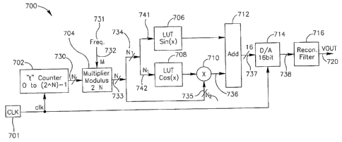
shown at 735). Using Ni (as a first portion of the N-bit phase word) a
corresponding
entry in LUT Sin(x) 706 and a corresponding entry in LUT Cos(x) 708 may be
accessed
(shown at 741 and 742, respectively), to obtain corresponding Sin(x) and
Cos(x) values
in relatively small sized LUTs, with only2" lines or entries (instead of 2"
lines or
entries). In our example, a 10-bit (N, =10) address word yields 1024 lines or
entries in
LUT Sin(x) 706 and 10241ines or entries in LUT Cos(x) 708. The N2 - bit word
(which
is a second portion of the N-bit pllase word, shown at 735) may represent Ax
and is
multiplied by phase error multiplier 710 with the corresponding value in an
entry in LUT
Cos(x) 708, to obtain (shown at 736) a small correction factor to the sin(2
';r'~" }
2
calculation (a phase-related error data).
-28-
CA 02573707 2007-01-11
[0067] The values of N, and N2 are defined according to two considerations. On
one
hand N, should be kept as minimal as possible in order to keep LUT Sin(x) 706
as small
as possible. On the other hand, the value of N2 (=N- Ni) should be also kept
as minimal
as possible in order to keep the approximation enor ( r,x ) to a minimum. For
a given
application, the minimal usable, or allowable, value of N, may be obtained
using
mathematical simulation that will show the spurious signal level resulting
from this
approximation error ( Ax ). If the value of Ni is smaller than the 'minimal
usable value of
Nl', the approximation in expression (8) will not suffice, which will result
in a
reconstructed output signal that will deviate from the ideal (pure), or nearly
ideal,
sinusoidal waveform. In the context of the present disclosure a non-ideal
sinusoidal
waveform introduces unwanted signals that are called 'spuriouses'. After
setting the
value of N i, the value of N2 is set to be N- Ni N. It has been found in
simulations tliat, for
many applications, a value of N, = 10 is more that sufficient, and that the
resulting
LUTs' size is minimal [2K-memory size, witli 16-bit long digital words). In
order to
generate a digital signal corresponding to the required Sin(x+Ax) value
approximation, as
detailed in the approximation formula above, an adder (shown at 712) is used
to sum up
the digital Sin(x) data generated by LUT Sin(x) 706 with the output of error
multiplier
710 that generates data that corresponds to the value of Cos(x) (generated by
LUT Cos(x)
708) multiplied by the error factor N2 which is the LSB part of the binary
number
received from phase multiplier 704. Now, the calculated voltage output (in
digital
format) of adder 712 is fed (shown at 737) to k-bit DAC 714 ('k' may be, for
example,
16), which generates and outputs (sliown at 738) an analog signal with the
required
frequency and phase. The analog signal output by k-bit DAC 714 is then fed
(shown at
738) to reconstruction filter (LPF) 716, to reduce unwanted frequency
harmonics and to
-29-
CA 02573707 2007-01-11
maintain the resulting output signal (at 720) substantially at constant
amplitude. In most
practical cases, where the maximum frequency of the generated signal (at 720)
is
considerably lower than the frequency FccK of the external clock,
Reconstruction filter
716 may be relatively simple.
[0068] Referring now to Fig. 8, a high-level flowchart for generating a phase
coherent
signal is shown and described according to an embodiment of the present
disclosure. At
step 801, a phase word is generated as described in connection with Fig. 7. A
first portion
of the phase word may be used for accessing, at step 802, an entry in Sin(x)
and Cos(x)
LUTs. A second portion of the phase word may be used to generate, at step 803,
a phase-
related error data. The phase-related error data, which may be obtained in the
way
described in connection with Fig. 7, may be added, at step 804, to a value
stored in an
entry of the Sin(x) LUT associated with (accessed using) the first portion of
the phase
word, whereby to generate a digital word from which a corresponding analog
value of a
sinusoidal may be generated, at step 805. After obtaining an analog value that
corresponds to the current time instant, a following analog value may be
likewise
generated, by repeating (shown as loop 810) steps 801 to 805, for the next
time instant,
which is specified by the time word generated by a time counter such as the
time-counter
702 shown in Fig. 7.
[0069J The avowed goal of the present disclosure, of maintaining phase
coherency when
frequency changes occur in an output signal, is obtained because, regardless
of the
application of the M-bit control word (shown at 732 in Fig.. 7) to set a
designated or
required frequency (shown at 731 in Fig. 7) and the instant(s) at which the M-
bit control
-30-
CA 02573707 2007-01-11
word is applied, the values of the signal's phase always equal 21r *. f * t.
The counter's
(shown at 702 in Fig. 7) instantaneous value (within the designated counting
range)
represents the time elapsing from the activation of the time counter, and the
elapsing time
does not depend on frequency changes. For example, assuming that the output
signal's
frequency of a frequency synthesizer (such as frequency synthesizer 700) is
initially set
to fl at time tl, the instantaneous phase of the output signal at instant tl
will be
2r * f, * t, . Then, assuming that at instant t2 the frequency of the
frequency synthesizer
changes from fl to f2, the instantaneous phase of' the output signal at
instant t2 will have
a value 21r *, f, * tZ that differs from the phase value at t2 associated with
frequency fI
(27r *, f i* t, ). Assuming that at instant t3 the frequency of the frequency
synthesizer
returns (changes back from f2) to fl, the instantaneous phase of the output
signal at
instant 0 will have a value 2;r * f, * t, which is a value that would have
been reached
spontaneously, as if no frequency changes occurred from f1 to fZ and from f2
back to fl.
In this manner, the novel DDS circuit disclosed in the present disclosure
maintains the
pliase-coherency of the output signal.
[0070] While certain features of the disclosure have been illustrated and
described
herein, many modifications, substitutions, changes, and equivalents will now
occur to
those skilled in the art. It is, therefore, to be understood that the appended
claims are
intended to cover all such modifications and changes as fall within the true
spirit of the
disclosure.
-31-