Note: Descriptions are shown in the official language in which they were submitted.
CA 02573981 2007-01-15
WO 2006/019369 PCT/US2004/022755
A PRIVATE AND SECURE OPTICAL COMMUNICATION SYSTEM
USING AN OPTICAL TAPPED DELAY LINE
FIELD OF THE INVENTION
[0001] The present invention relates generally to optical systems, including
what may be referred to as optical communications systems, optical
telecommunications systems and optical networks, and more particularly to a
method
and system for information security in an optical transmission system.
BACKGROUND OF THE INVENTION
[0002] Optical telecommunications is a primary method of transporting
information around the world. Wavelength Division Multiplexing (WDM)
technology has led to as many as 80 and 160 information-carrying wavelengths
on a
single fiber at bit rates as high as 10 and 40 gigabits per second per
wavelength.
While this increase in througliput and capacity is impressive, security is
becoming '
increasingly important as the use of fiber.optic WDM and free space optical
telecommunication systems continue to expand.
[0003] Most existing methods of protecting an optical transmission encrypt a
signal in the electrical domain before the signal is transferred to the
optical layer. For
example, in van Breeman et al, U.S. patent 5,473,696, the data stream is
enciphered
by adding, modulo 2, a pseudorandom stream before transmission and recovering
the
data by addition of the same pseudorandom stream. Rutledge, U.S. patent
5,864,625,
electronically encrypts the information and optically transmits a security key
used for
the encryption process. These types of protection systems are limited by the
electronic processing rate, currently, no better than approximately 2.5 to 10
gigabits
per second. Secondly, these electronic methods of protection are costly to
implement
and can create latency issues.
[0004] Brackett et al in U.S. patent 4,866,699 teaches an analog method of
coding and decoding for multi-user communications based on optical frequency
domain coding and decoding of coherently related spectral components. Brackett
fails
to address any secure or privacy communication applications where the spectral
components are not coherently related.
[0005] In view of the foregoing, one object in accordance with the present
invention is to improve optical communications security by providing an analog
-1-
CA 02573981 2007-01-15
WO 2006/019369 PCT/US2004/022755
method of protecting transmissions that is lower in cost, volume, weight
and/or
power, especially at higli transmission bit rates.
SUMMARY OF THE INVENTION
[0006] The present invention, in a preferred embodiment, provides an analog
metliod and apparatus for effectively protecting electronic communications
that may
be transmitted, for example, over a fiber optic or free-space network. In a
preferred
embodiment the present invention may use a combination of an Optical Tapped
Delay
Line (OTDL), as disclosed in U.S. patent 6,608,721 (which patent is
incorporated
herein by reference), with known methods of altering the properties of an
analog
signal.
[0007] A privacy system can be described as a system where the source signal
is sufficiently protected to make unauthorized interception exceptionally
difficult for
the majority of potential adversaries, but not so difficult as to prevent
interception by,
a sophisticated, well-funded and determined adversary, such as a government. A
secure system is one in which the transmitted information signal is well
protected
against i.uiauthorized intrusion by highly sophisticated adversaries having
extensive
computing resources. The security provided in accordance with the present
invention
can attain many levels of security, from a privacy system to a truly secure
system, by,
for example: (1) varying the number of sub-bands; (2) changing the analog
properties
of the sub-bands by altering the phase, introducing time delays, or shifting
the
originating signal's frequency components; and (3) controlling the periodicity
of the
changes.
[0008] The rate of signal transmission also affects the probability of signal
interception. For example, a 10 gigabit per second signal is inherently more
difficult
to intercept than a 2.5 gigabit per second signal. The present invention, in a
preferred
embodiment, is capable of protecting optical signals at bit rates exceeding 1
gigabit
per second.
[0009] A transmission using a preferred embodiment of the present invention
is protected from an attack because any attack requires coherent detection of
a large
bandwidth of analog data at a high-precision digitization rate, and even if
coherently
intercepted, the properties of the signal are scrambled to the extent that
recovery is
virtually impossible. For example, an OTDL device with 128 sub-bands and 10
different phase shift combinations, requires a brute-force attack approaching
10128
-2-
CA 02573981 2007-01-15
WO 2006/019369 PCT/US2004/022755
tries to coherently recover the signal, a feat not possible with current
analog-to-digital
conversion technology combined with the fastest supercoinputer. To make
interception even less likely, the sub-band distortion pattern can be
periodically
changed.
BRIEF DESCRIPTION OF THE DRAWINGS
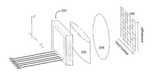
[0010] Figure 1 illustrates an example of an Optical Tapped Delay Line
(OTDL).
[0011] Figure 2 illustrates an example of an operational side view of an OTDL
device.
[0012] Figure 3 illustrates an example of an operational side view of a
preferred embodiment of the present invention operating in reflective mode.
[0013] Figure 4 illustrates an example of a signal before, during and after
transmission through a preferred embodiment of the present invention.
[0014] Figure 5 illustrates an example of a preferred embodiment of the
present invention in transmissive mode. '
[0015] Figure 6 illustrates an example of an input carrier frequency shifting
embodiment of the present invention in reflective mode.
[0016] Figure 7 illustrates an example of an input carrier frequency shifting
embodiment of the present invention in transmissive mode.
[0017] Figure 8 illustrates an example of another embodiment of the present
invention that uses two OTDL devices to obtain very high resolution'sub-bands.
DETAILED DESCRIPTION
[0018] Figures 1 and 2 illustrate examples of the previously referenced OTDL
device for demultiplexing a multi-channel WDM band into individual channels. A
detailed explanation of the device is provided in U.S. patent 6,608,721
(incorporated
herein by reference), but the operation will be briefly outlined here to
facilitate
understanding of some preferred embodiments of the invention. In the
illustrated
example, six collimated input beams 230a - 230f enter an Optical Tapped Delay
Line
(OTDL) 231. The origin of the beams may be, for example, the collimated
outputs of
six optical fibers (not shown) where each fiber typically carries multiple
wavelengths.
A fully reflective coating 232 on plate 235 and a partially reflective coating
236 on
plate 237 cause each of the input beams entering the device to be multiply
reflected
within a cavity 233. A portion of each beam, a beamlet, exits the cavity at a
plurality
-3-
CA 02573981 2007-01-15
WO 2006/019369 PCT/US2004/022755
of taps 240a - f, with each succeeding exiting portion being time delayed with
respect
to the preceding portion.
[0019] The various output beams are then directed to an anamorphic optical
system having a cylinder lens 242 and a spherical lens 245. The anamorphic
optical
system 242, 245 performs the functions of: 1) Fourier transformation of the
output of
the cavity 231 in the vertical dimension y, and 2) imaging of the output beams
of the
OTDL 231 in the horizontal dimension x onto an output surface 246. The outputs
are
imaged on plane 246 with each information-carrying wavelength focused at a
specific
spot on the plane. By properly placing detectors at plane 246, each WDM
information channel may be detected for further processing.
[0020] Figure 3 illustrates an example of an optical communications system in
accordance with a preferred embodiment of the present invention. This
einbodiment
includes a transmitter 50 and areceiver 52. A fiber 56 carrying an infonnation-
carrying optical signal is received by the OTDL 58. The liglit is processed as
described in the explanation for Figures 1 and 2. The beamlets exit the OTDL
from
optical tap locations 54a to 54g and a lens system 60 interferes the beamlets
onto a
planar reflective phase modulator array 62., Passage through the OTDL 58 and
lens
60 to the plane 62 has split the information-carrying optical signal into a
number of
sub-bands. The OTDL can be designed to output at least hundreds of sub-bands.
[0021] The reflective phase modulator array 62 may be implemented in a
number of ways, including, but not limited to, a liquid crystal array, a MEMS
device,
or an array of III-V or II-VI semiconductor devices. The speed at which the
phase
shifting changes may directly affect the level of security afforded. In this
example
one modulator element is associated with each sub-band. As each sub-band
passes
through a modulator element, it is phase shifted in a manner determined by the
control
coinputer 64. The mirror part of the modulator array 62 reflects the sub-bands
back
through lens system 60 to tap locations 57a to 57g. The OTDL 58 recombines the
taps into an optical signal for retransmission over a fiber optic carrier 76
to the
destination.
[0022] The signal from transmitter 50 is received by OTDL 72 from fiber 76.
The OTDL 72 and lens 70 combination is identical to the OTDL 58 and lens 60
combination. OTDL 72 and lens 70 separate the signal into the identical sub-
bands
created by OTDL 58 and lens 60. The sub-bands are imaged onto the reflective
phase
modulator array 68, with each array element receiving the same sub-band as the
-4-
CA 02573981 2007-01-15
WO 2006/019369 PCT/US2004/022755
corresponding modulator in array 62. The control computer 66 causes each sub-
band
to be phase shifted in the opposite manner as instructed by control computer
64. Each
sub-band is then reflected back through lens system 70 to OTDL 72 which
together
recombine the sub-bands into a single signal that is output to fiber 74 for
further
processing or routing.
[0023] The effect of imparting a phase shift to each sub-band is to introduce
distortion. If the amount of distortion is sufficient, the information content
becomes
undecipherable and security is enhanced. The control computer 64 instructs the
modulator array how to modify the phase of the sub-bands in a manner that is
unpredictable to anyone not having knowledge of the computer input. The rate
at
which the phase shifts are changed depends upon the level of security
required. A
fixed phase shift pattern will sufficiently distort the signal to make it
incomprehensible; however, determined interceptors can analyze the signal and
eventually determine, and reverse the effects of, the phase shift pattern. To
ensure
continued security, the fixed phase shift pattern can be changed occasionally,
requiring the potential interceptor to start the analysis over again. For the
highest
security, this change must be made often enough to guarantee that even with
the
highest performance computational systems anticipated, the phase shifts do not
remain static long enough for any lcnown analysis to succeed before the
pattern
changes. A secure system will result if the phase shifter array settings 62
and 68 in
Figure 3 are changed at least as fast as twice the time aperture required for
an
interceptor to compute the settings.
[0024] Preferably, the computer input to the phase modulators may be derived
from a deterministic algorithm, the starting point of which may be derived
from a key
setting provided to the computer. This permits a receiver having knowledge of
both
the algorithm and the key setting to reproduce the same control computer
signal, and
thereby, reverse the phase distortions and recover the information signal
intact.
[0025] For purposes of illustrating the principles of this embodiment of the
invention, only a single signal or channel has been described. However, using
the
multi-port interleaving capability of the OTDL, as described in U.S. patent
6,608,721
(incorporated herein by reference), embodiments in accordance with the present
invention are capable of simultaneously encrypting all channels of a multi-
channel
WDM communications system. As used herein the term "encrypting" includes all
levels of security from low-security to the highest levels of certified
security.
-5-
CA 02573981 2007-01-15
WO 2006/019369 PCT/US2004/022755
[0026] For the illustrated embodiment of the present invention to be optimally
effective, the sub-band resolution, i.e., the spacing between each sub-band at
focal
plane 62 ofthe OTDL in Figure 3, should be significantly finer, preferably at
least 10
times finer, and more preferably at least 50 times finer, than the bandwidth
of the
input signal. In this particular embodiment, for example, if the input signal
has a bit
rate of 10 gigabits per second, the design of the OTDL should be at least 50
sub-bands
with a spatial resolution at the focal plane of 200 MHz or finer.
[0027] Each array element may see a portion of the signal in the frequency
domain, defined by the equation:
F(t, K) = f wa+1 T
~~ fo f(S+t) e'~'sdS dr.o
[0028] where
i. t aperture of the hyperfine device (tap key)
ii. S time integration variable
iii. co = frequency
iv. K = sub-band index
[0029] Defining
L'(o), t) = f T f(S + t) eJ~'sdS
[0030] as a sliding Fourier transform (e.g., block of data), 'If ((O,t) may be
perceived as that spectral component of the information signal incident on an
element
of the reflective phase shifter.
In a preferred embodiment, the present invention imparts a phase shift to each
spectral component hitting a specific array element. Specifically, each array
element
sees a signal defined as a complex number
-6-
CA 02573981 2007-01-15
WO 2006/019369 PCT/US2004/022755
Ae''P
where (p is the entity to be altered by the phase shifter of the invention. In
another
embodiment, it would be possible to alter A(amplitude) instead of cp, but
doing so
would result in a loss of power and, potentially, information content.
Altering cp does
not produce a power loss, nor is any information content lost.
[0031] Figure 4 is a simulated example illustrating the transmission of the
signal in Figure 3. 57 is a representation of the original signal carried on
fiber 56.
After being phase shifted by transmitter 50, the transmitted and distorted
signal
appears as shown by 77. After passing through receiver 52, the signal is
output on
fiber 74 and appears as shown by 75, identical to the incoming original signal
57.
[0032] The embodiment illustrated in Figure 3 is a reflective architecture of
the present invention that utilizes the reversibility property of an OTDL,
whereby,
only one OTDL device is used for transmitting and receiving. An alternative
einbodiment of the present invention is a transmissive architecture
illustrated in
Figure 5 where two OTDL devices comprise the transmitter 200 and two OTDL
devices coinprise the receiver 210. The phase shifter arrays 84 and 94 for
this
architecture are transmissive versus reflective. OTDL 100 combines the
distorted
signal into a signal for transmission on fiber 90. This signal is received by
OTDL 101
from fiber 90 and, together with lens 60, separates the signal into the
identical sub-
bands created by OTDL 99 and lens 61. These sub-bands are passed through the
transmissive phase shifter 94 and to lens 87 and OTDL 102 for recombining as
the
original undistorted signal.
[0033] As mentioned earlier, there are two other possible types of distortion
techniques: (1) introduction of a random time delay; or (2) frequency shifting
the sub-
bands. A signal delay could be created by a coil, white cell, loop in a
waveguide, or
other types of free space delay. There are many methods to shift the frequency
of an
optical signal, such as using stimulated Brillouin Scattering, four wave
mixing, three
wave mixing, or use of any optical modulator device, such as a lithium niobate
Mach-
Zender, indium phosphide electroabsorption, electroabsorption multi-quantum
well or
an electrorefraction device. Note that the values of the frequency shifts
applied must
meet other constraints in order to be feasible for the embodiment used. Each
of the
-7-
CA 02573981 2007-01-15
WO 2006/019369 PCT/US2004/022755
three methods of signal distortion could be used independently or in any
combination
to produce a private or secure optical transmission system.
[0034] Another preferred embodiment of the present invention involves
destroying the coherence of the input carrier by shifting the frequency of the
input
source. Again, any of the previously mentioned in-line distortion techniques
could be
used in coiubination with this method. Figure 6 shows an example of a
reflective
architecture in accordance with this method. Figure 7 shows an example of a
transmissive architecture in accordance with this method.
[0035] As illustrated in the example of Figure 1, the OTDL may be a two-
dimensional device, i.e., the OTDL may sub-channelize an optical signal from
multiple fiber optic inputs shown as 230a through 230f producing a matrix of
sub-
bands and input fibers at the focal plane. Another method to obtain a higher
level of
security may be to use the previously described methods of distorting the sub-
bands
but also send the sub-bands out on differing outputs.
[0036] A further enhancement in security may be obtained using an OTDL in
the architecture described in U.S. patent 6,608,721 B1 (incorporated herein by
reference) and shown in Figure 8, where OTDL 160 is rotated 90 degrees from
the
orientation of a first OTDL 150. The first OTDL generates a coarse sub-
banding.
The second OTDL further subdivides each sub-band into finer sub-bands. This
architecture creates a large number of very fine sub-bands of the incoming
signal.
The distortion metliods previously discussed could be applied to each of the
sub-
bands at location 170. The very finely and distorted sub-bands could be
recombined
into a signal using the transmissive or reflective architecture disclosed
previously for
transmission to the destination. A receiver architecture using the design in
Figure 8
would separate the very fine sub-bands, reverse the distortion and recombine
the
undistorted sub-bands into a signal.
-8-