Note: Descriptions are shown in the official language in which they were submitted.
CA 02574835 2007-01-22
WO 2006/110159 PCT/US2005/026840
MICRO NEUTRON DETECTORS
This application claims priority to and the benefit of U.S. Provisional
Application No. 60/592,314, filed July 29, 2004.
Statement of Government Rights
The invention was partially funded by the U.S. Government, under the
Department of Energy, Nuclear Energy Research Initiative (NERI) Grant
Number DE-FG03-02SF22611. Accordingly, the U.S. Government may
reserve certain rights to its use.
Field of the Invention
This invention relates generally to radiation detectors. In particular, the
invention relates to semiconductor detectors designed to detect neutrons of
various energy ranges. More particularly, the invention relates to micro
neutron detectors useful for the real-time monitoring of both near-core and in-
core neutron fluxes of nuclear reactors.
Background of the Invention
Nuclear reactors convert mass into energy. Although nuclear fusion
I
CA 02574835 2007-01-22
WO 2006/110159 PCT/US2005/026840
provides an alternative means of energy production, limitations in scientific
understanding currently limit energy production to those reactors utilizing
nuclear fission. Nuclear fission occurs when an atom breaks apart, either
spontaneously or due to some disruptive force. The total mass of the resulting
products, usually two smaller atoms or nuclei and one or more neutrons, is
less
than the mass of the initial atom. The energy emitted by the reaction directly
correlates to the difference in mass between the two objects according to the
relationship E=m*c2. Importantly, within a nuclear reactor, the neutrons
emitted as a result of the reaction radiate until they come in contact with
another object. When this object is an atom susceptible to fission, the
collision
provides the disruptive force necessary to instate division of the atom. The
second division emits additional neutrons, as does each additional division,
resulting in a chain reaction. Thus, the energy generated in a given location
relates directly to the corresponding neutron flux.
Presently, the state of the art of neutron detectors for reactors
contemplates a variety of materials and sizes. For instance, small
semiconductor detectors, such as Si, bulk GaAs and diamond detectors,
subsequently coated with neutron reactive materials have been investigated.
While they achieve advantage with their small size and compactness, they
generally catastrophically fail for neutron fluences that are much too low for
in-
core/near-core routine neutron measurements, except perhaps for a few, such as
SiC or amorphous Si. Gas-filled chambers, on the other hand, with 235U added
as a film coating or as an internal foil, for example, are used to measure
high
neutron fluxes near a reactor core. Advantageously, these devices are
radiation
hard and are insensitive to gamma ray background. Disadvantageously, they
generally require relatively high voltages and are quite large. Appreciating
2
CA 02574835 2007-01-22
WO 2006/110159 PCT/US2005/026840
some of the smaller still have chamber sizes on the order of 1200 mm3 or more,
this makes response times relatively very slow, hence adding to detector dead
time. Further, the devices are too large to be used as single point detectors
for
back-projection calculations. Still other devices, known as "self-powered"
detectors, are generally manufactured from rhodium or vanadium and used for
in-core reactor measurements. While these devices can be inserted in tiny
areas
and are relatively insensitive to gamma ray background, they cannot provide an
immediate response to a change in a reactor's neutron flux. Instead, rhodium
and vanadium detectors, which rely on the radioactive decay of a neutron
activated material, provide only an average value and can take up to 5 minutes
to reach equilibrium.
Accordingly, there is a need for small compact neutron detection devices
that can be used for in-core, real-time neutron flux measurements of both
power and naval nuclear reactors. Simultaneously, however, the devices must
be small enough so as to easily fit within the constraints of the reactor core
physical design and have adequate sensitivity to the neutron flux while not
perturbing the neutrons so as to alter reactor operations. In other words, the
devices cannot be so large that they absorb too many neutrons and thereby
affect the neutron chain reaction of the reactor.
Summarv of the Invention
The above-mentioned and other problems become solved by applying
the principles and teachings associated with the hereinafter described micro
neutron detectors.
3
CA 02574835 2007-01-22
WO 2006/110159 PCT/US2005/026840
In one aspect, the micro neutron detectors have relatively small size and
include pockets, for containing a gas, having a volume on the order from a few
cubic microns to 1200 mm3. A neutron reactive material, such as a fissionable,
fertile or fissile material or combinations thereof, like 235U, 238U, 233 U,
232Th,
239 Pu, loB, 6Li or 6LiF, is in contact with the gas and an electrical bias is
placed
across the pocket. In this manner, neutron interactions in the reactive
coating
cause charged particles to eject in opposite directions. When these energetic
ionizing particles enter the gas pocket, they produce ionization in the form
of
electron-ion pairs. In turn, the applied voltage causes the positive ions and
the
electrons to separate and drift apart, electrons to the anode and positive
ions to
the cathode. The motion of the charges then produces an induced current that
is sensed and measurable, thereby indicating the presence of neutrons.
Preferably, the result embodies a measurable pulse indicating the presence of
a
neutron having been interacted in the detector.
In another aspect, the detectors are physically arranged as two
clamshelled sections, three sandwiched supports, an array of a multiplicity of
detectors, a triad of detectors each capable of performing a different
detecting
function and/or a variety of capillary channels formed in substrates. Specific
clamshelled section embodiments include two insulator halves with openings
joined together to form a pocket. On a surface of one or both of the insulator
halves, a coating of a neutron reactive material is applied. A conductive
coating contacting the neutron reactive material is further applied and
fashioned with electrical leads to ultimately apply a bias across the pocket
and
neutron reactive coating during use. Specific sandwiched support
embodiments include three supports with an interior support having openings
that form a gas pocket. Coatings of the neutron reactive material and
4
CA 02574835 2007-01-22
WO 2006/110159 PCT/US2005/026840
conductors are applied on the exterior supports in the vicinity of the
openings
and, when fastened/sandwiched, create a gas pocket capable of having an
electrical bias applied across. Specific triads of detectors embody the
foregoing three supports with three openings in the interior support. In the
vicinity of two of the three openings, neutron reactive materials and
conductor
materials are applied on the exterior supports. However, one of the openings
clearly lacks such coatings. Also, the coatings of neutron reactive materials
differ from one another so that each detector can serve a different detecting
role. Namely, fast or thermal neutron detection. The opening without a
neutron reactive coating, in turn, serves as a background or baseline reading
detector. Specific embodiments of capillary channels contemplate multiple
substrates etched to create a plurality of peaks and valleys so that upon
joining,
the substrates matingly define pluralities of pockets for receiving/containing
gas. The unique capillary channel design allows for signals to be extracted
from individual detectors along each channel. Further, unlike multi-wire gas
detectors, the walls separating the channels prevent excited charges from
entering the detector space of an adjacent channel, hence preventing
electronics
signals being shared between two or more detectors, an effect often termed as
"crosstalk." Also, a neutron reactive material is applied to one or both of
the
substrates as well as various conductive coatings for facilitating the
electrical
bias across the pocket. Certainly, thin film and VLSI techniques are
contemplated in this regard. Regardless of type, preferred gases in the
detectors variously include argon, P-10, 3He, BF3 and mixtures of argon, He,
BF35 C02, Xe, C4H1o, CH4, C2H6, CF4, C3H8, dimethyl ether, C3H6 and C3H8.
Methods of making the detectors broadly include providing a gas
environment, assembling a neutron reactive material to form at least a portion
5
CA 02574835 2007-01-22
WO 2006/110159 PCT/US2005/026840
of a pocket therein and sealing the pocket. Then, upon removal of the pocket
from the gas environment, the pocket retains the gas of the gas environment.
Further manufacturing techniques include coatings of uranyl and thorium
nitrate applied via thin film deposition, vapor depositions such as
evaporation
with electron-beam techniques, sputtering, or the like.
In still alternate embodiments of the invention, one or more detectors are
provided directly with one or more fuel bundles for use in a reactor. In this
manner, upon inserting the fuel into the reactor, detectors are also inserted
and
provide an instantaneous in-core neutron flux measurement capability. During
use, this also adds to reactor fuel efficiency increases because real-time
adjustments of fuel bundle location or locating spotty fuel burn-up, for
example, can be made based on the output readings of the detectors.
Appreciating average fuel bundles cost hundreds of thousands of dollars or
more, the more effective burning of fuel will certainly save money too.
Further, upon removal of the fuel bundle from the reactor, after use, the
detectors can remain with the bundle and later provide an indication of the
state
of the bundles, such as before/during transportation to waste sites. Operating
nuclear reactors with detectors disposed in their moderator are also
contemplated with and apart from the detectors with the fuel bundle
embodiment. Flux mapping of the core also results with these detectors
regardless of use with the fuel bundle. In turn, mapping results in learning
core
efficiencies, for instance.
With more specificity, it is expected that many detectors will be placed
at various positions throughout the core of the nuclear reactor and it will
become possible to generate a three-dimensional (3-D) map of the neutron flux
within the core. In one instance, several detectors will be placed on a rod,
for
6
CA 02574835 2007-01-22
WO 2006/110159 PCT/US2005/026840
example. Each rod will then be placed at a position within the reactor core.
By
monitoring the readings from each detector, the position of which is known,
plotting programs can generate a 3-D map of the real-time neutron flux
throughout the core. Since some detectors may embody a triad serving the
simultaneous role of detecting fast and thermal neutrons, and distinguishing
same from the background, the 3-D map will also have the capability of
superimposition in that a 3-D map of thermal neutron flux, can be
superimposed upon a 3-D map of fast neutron flux, which in turn can be
superimposed upon a 3-D map of the gamma ray flux. Heretofore, this was
unknown. Also, this map will be useful for showing any unevenness within the
core, any spurious problems, or any additional problems associated with
neutron/gamma ray fluxes.
In a broad sense, the many embodiments of micro neutron detectors of
-the invention overcome the problems of the prior art and provide neutron
radiation detection in a manner, heretofore unknown, capable of simultaneously
withstanding intense radiation fields, capable of performing "near-core" and
"in-core" reactor measurements, capable of pulse mode or current mode
operation, capable of discriminating neutron signals from background gamma
ray signals, and tiny enough to be inserted directly into a nuclear reactor
without significantly perturbing the neutron flux. Advantageously, the
invention accomplishes this with a new type of compact radiation detector
based on the fission chamber concept and is useful for at least three specific
purposes: (1) as reactor power level monitors, (2) power transient monitors,
and (3) real-time monitoring of neutron flux profiles of a reactor core. The
third application also has the unique benefit of providing information that,
with
inversion techniques, can be used to infer the three-dimensional distribution
of
7
CA 02574835 2007-01-22
WO 2006/110159 PCT/US2005/026840
fission' neutron production in the core. Additional uses of the disclosed
invention may include the detection of nuclear weapons, weapons-grade
plutonium, or both.
It is important to reiterate that the micro neutron detectors proposed
herein are unique because of their miniature size and rapid response time.
Some of the important features, but by no means limiting, include,:
1. Compact size - the dimensions of the micro neutron detectors are
small, similar to semiconductor devices, and easy to operate in tight
environments. Compactness also enables simultaneous use of pluralities of
detectors thereby building in neutron detection redundancy.
2. Thermally resistant - the micro neutron detectors can be
manufactured from high-temperature ceramics or high temperature radiation
resistant materials that can withstand the high-temperatures and harsh
environment of a nuclear reactor core.
3. Gamma ray insensitive - the detection gas, small size, and light
material composition all work to make the device gamma ray insensitive, hence
the neutron signals output from the micro neutron detectors will be easily
discernable from background gamma ray interference. As a result, the
detectors naturally discriminate out gamma ray background noise from neutron
interactions.
4. Inexpensive - construction is straightforward and requires
inexpensive materials, such as aluminum oxide or oxidized silicon;
construction also takes advantage of well known techniques such as thin film
deposition and VLSI processing techniques.
5. Large signals - the reaction products are highly energetic and the
output signals of the micro neutron detectors are easy to detect.
8
CA 02574835 2007-01-22
WO 2006/110159 PCT/US2005/026840
6. Radiation hardness - the structure of the detectors is radiation
hard because the electronic material is a gas, not a solid, hence it does not
undergo structural damage. The detectors survive neutron fluences 1,000 times
greater than that which prior art semiconductor devices are capable of.
~
7. Low power requirement - the detectors preferably operate with
applied biases as low as 20 volts; ranges include about 1 to about 1000 volts.
8. Tailored efficiency - the detectors can be constructed to have low
(<0.001 %) efficiency up to 7% efficiency such that it can be used for several
different applications.
9. Deployment at Power Reactors - Successful demonstration of the
detectors is leading to detector usage in the nuclear industry, including
naval
and commercial nuclear reactors with practical applications contemplating: 1)
nuclear reactor core instrumentation for the present power industry; 2)
nuclear
reactor core instrumentation for naval reactor vessels; 3) imaging arrays for
neutron imaging at neutron radiography ports; 4) imaging arrays for neutron
sensing at neutron scattering centers such as the DOE Spallation Neuron
Source; 5) nuclear fuel bum-up monitors in power reactors; 6) localized point
flux monitors for reactors and beam ports; and 7) regulation of nuclear
weapons.
In the regulation of nuclear weapons, neutron detection requirements for
support of arms control agreements pose challenges that conventional detector
designs cannot meet. For example, detector designs must be able to determine
the number of Reentry Vehicles (RV) in an assembled missile without
removing the aerodynamic shield or collecting critical nuclear weapons design
information (CNWDI). Further, the technology must meet the approval of all
treaty partners. One treaty partner, Russia, is particularly sensitive about
new
9
CA 02574835 2007-01-22
WO 2006/110159 PCT/US2005/026840
high technology detectors, fearing that they could be subverted for
intelligence
gathering applications. Currently, a neutron detector designed by Sandia
National Laboratory is used for treaty confidence building tests, however it
does not have direction sensing capability, and cannot be used for this field
application. Nonetheless, since all parties have found a neutron detector
acceptable, one can reasonably assume that a directional sensitive neutron
detector would also be acceptable.
Incorporating the teachings of the instant invention, a radiation-
hardened neutron-imaging device can be produced. The new devices can have
directional dependence that can be used to assess the origin of the neutrons.
The neutron radiation imaging detectors are gamma ray insensitive, have high
spatial resolution, have relatively high neutron detection efficiency, are
compact in thickness, radiation hard, and are capable of imaging large areas.
In this regard, the inventors introduce a new array type of gas detector
that will operate well as an inexpensive, easily maintainable, neutron
detector
for both thermal and fast neutron fields. The expected high sensitivity of the
detector and flat plate design may make it useful for detecting the presence
of
highly enriched uranium (HEU) and weapons grade plutonium (WGPu) in
packages as well as imaging support for neutron physics experiments at
national laboratory facilities. With such configuration, the sensitivity
should be
sufficient to identify WGPu in reasonably sized packages with or without
active interrogation of the package with a neutron source. Because the count
rate is expected to be low, and also because the design keeps the volume of
the
detection gas low, it should be possible to charge the detector with gas and
use
it without a gas recharge for as long as 24 hours. Other variations can use
continuous gas flow as the source. The new detector will also permit high-
CA 02574835 2007-01-22
WO 2006/110159 PCT/US2005/026840
resolution digital neutron radiography on objects where photon radiography is
impossible, and will permit further advances in nuclear physics and
engineering
by the availability of inexpensive neutron detectors that can be optimized to
their requirements.
Additional benefits of the current invention in the foregoing regard,
especially embodiments having pockets as capillary channels, include but are
not limited to:
1. Directionally Dependent - Neutrons incident on the front face of
the detector will be detected while the thickness of the detector, generally,
makes interactions from the sides unlikely.
2. High-spatial resolution - the spatial resolution is determined by
the strip pitch.
3. Gamma ray insensitive - gas-filled or gas-flow detectors are
typically insensitive. to gamma rays. The large signals produced by the
fission
fragments will be easily discriminated from any gamma ray events.
4. No cross talk - pockets as capillary channels have walls
substantially preventing charges from entering adjacent regions.
5. Compact - the detectors will be only a few millimeters thick.
6. Large area - substrates can be 8 or more inches in diameter.
7. Stackable for efficiency - the compactness enables stacking of
detectors to increase efficiency, if needed.
8. Neutron Energy - By placing different thickness of moderator
over different sections of the detector, a rough estimate of the incident
neutron
energy can be made.
Rrief Descrintion of the Drawinuc
It
CA 02574835 2007-01-22
WO 2006/110159 PCT/US2005/026840
Figure 1 is a diagrammatic view in accordance with the present
invention of a representative micro neutron detector formed, for example, as
two halves;
Figure 2 is a diagrammatic view in accordance with the present
invention of an assembled and operational micro neutron detector of Figure 1;
Figure 3 is a diagrammatic view in accordance with the present
invention of an alternate representative of a micro neutron detector formed,
for
example, with three supports;
Figure 4 is a diagrammatic view in accordance with the present
invention of an assembled and operational micro neutron detector of Figure 3;
Figure 5 is a diagrammatic, cut away view in accordance with the
present invention of an assembled micro neutron detector according to Figures
3 and 4;
Figures 6a and 6b are diagrammatic views in accordance with the
present invention of representative array of a plurality of micro neutron
detectors;
Figures 7a and 7b are diagrammatic views in accordance with the
present invention of the array of Figures 6a and 6b including a protective
sleeve for insertion, perhaps, into a neutron environment;
Figure 8 is a diagrammatic view in accordance with the present
invention of an alternate representative array of a plurality of micro neutron
detectors fashioned as a triad;
Figures 9 -12 are diagrammatic views in accordance with the present
invention of a variety of supports for use in making a micro neutron detector;
12
CA 02574835 2007-01-22
WO 2006/110159 PCT/US2005/026840
Figure 13 is a diagrammatic view in accordance with the present
invention of an assembled array of micro neutron detectors including
additional
functionality;
Figure 14 is a graph in accordance with the present invention of energy
deposition and ranges for ' B reaction products in 1 atm of P-10 gas;
Figure 15 is a graph in accordance with the present invention of energy
deposition and ranges for 10B reaction products in a micro neutron detector;
Figure 16 is a graph in accordance with the present invention of a
thermal neutron reaction product spectrum taken with a prototype 10B-coated
micro neutron detector as a representative micro neutron detector;
Figure 17 is a graph in accordance with the present invention of energy
deposition and ranges for typical fission fragments in 1 atm of P-10 gas;
Figure 18 is a graph in accordance with the present invention of energy
deposition and ranges for typical fission fragments in a representative micro
neutron detector;
Figure 19a is a graph in accordance with the present invention of a
thermal neutron induced spectrum from a prototype micro neutron detector;
Figure 19b is a graph in accordance with the present invention of a
predicted thermal neutron induced spectrum, generated using a Monte Carlo
code based on various micro neutron detector dimensions;
Figure 20a is a graph in accordance with the present invention of a
prototype micro neutron detector count rate as a function of reactor power;
Figure 20b is a diagrammatic view in accordance with the present
invention of a side-view diagram of the Kansas State University TRIGA Mark
II nuclear reactor facility in which data of the instant invention has been
gathered;
13
CA 02574835 2007-01-22
WO 2006/110159 PCT/US2005/026840
Figure 20c is a top-view photograph in accordance with the present
invention of the reactor facility of Figure 20b, including showing the core
and
graphite moderator;
Figure 20d is a diagrammatic view in accordance with the present
invention of the reactor facility of Figure 20b showing the reactor core
arrangement, including fuel and grid plate openings and positions for
inserting/placing micro neutron detectors in-core;
Figure 21 is a diagrammatic view in accordance with the present
invention of an alternate embodiment of a micro neutron detector;
Figure 22 is a diagrammatic view in accordance with the present
invention of an assembled micro neutron detector of Figure 21, including an
enlarged view of representative neutrons interacting in a neutron reactive
material;
Figure 23 is a diagrammatic, perspective view in accordance with the
present invention of a portion of the micro neutron detector of Figures 21 and
22;
Figures 24a and 24b are diagrammatic views in accordance with the
present invention of two possible methodologies for patterning the micro
neutron detectors of Figures 21-23 such that gas can continuously flow through
the detectors;
Figure 25 is a diagrammatic, perspective view in accordance with the
present invention of an assembled embodiment of a micro neutron detector
showing gas flow;
Figure 26 is a diagrammatic view in accordance with the present
invention of an alternate method to assemble a micro neutron detector;
14
CA 02574835 2007-01-22
WO 2006/110159 PCT/US2005/026840
Figure 27 is a diagrammatic view in accordance with the present
invention of still another alternate method to assemble a micro neutron
detector;
Figure 28 is a diagrammatic view in accordance with the present
invention of yet another alternate method to assemble a micro neutron
detector;
Figure 29 is a diagrammatic view in accordance with the present
invention of an assembled micro neutron detector mounted for use on a printed
circuit board interconnected to external electronics and gas supplies;
Figure 30 is a diagrammatic view in accordance with the present
invention of yet another embodiment for making a micro neutron detector;
Figure 31 is a graph in accordance with the present invention of a
lifetime optimization of a neutron reactive material as a coating in a micro
neutron detector;
Figure 32 is a graph in accordance with the present invention of gamma
energy deposition in 500 m of 1 atm of argon gas;
Figure 33 is a diagrammatic view in accordance with the present
invention of a fuel bundle having a micro neutron detector and a nuclear
reactor including same;
Figure 34 is a diagrammatic view in accordance with the present
invention of an alternate fuel bundle having a micro neutron detector and a
nuclear reactor including same; and
Figure 35 is a diagrammatic view in accordance with the present
invention of a three-dimensional neutron flux map for a nuclear reactor
constructed from a plurality of micro neutron detectors.
CA 02574835 2007-01-22
WO 2006/110159 PCT/US2005/026840
Detailed nescriprinn of the Preferred Emhodimentc
In the following detailed description, reference is made to the
accompanying drawings that form a part hereof, and in which is shown by way
of illustration, specific embodiments in which the invention may be practiced.
These embodiments are described in sufficient detail to enable those skilled
in
the art to practice the invention, and it is to be understood that other
embodiments may be utilized without departing from the scope of the
invention. The following, therefore, is not to be taken in a limiting sense,
and
the scope of the present invention is defined only by the appended claims and
their equivalents. In accordance with the present invention, varieties of
micro
neutron detectors and their methods of making and using are hereafter
described.
As a preliminary matter, the inventors investigated a variety of neutron
reactive materials and their properties for use in making and using micro
neutron detectors. As skilled artisans appreciate, only neutrons within
certain
energy levels will result in detection for a given detector. For example,
thermal
neutrons (0.0259 eV) absorbed by 10B produce energetic charged particles,
emitted at a 1800 angle, with a 94% probability of producing a 1.47 MeV a-
particle and an 840 keV 7 Li ion, and a 6% probability of producing a 1.78 MeV
a-particle and a 1.0 MeV 7 Li ion. The 2200-m/s neutron microscopic
absorption cross-section is 3840 barns, and the microscopic absorption cross-
section (a) follows an inverse velocity dependence over much of the thermal
energy range. The macroscopic thermal neutron absorption cross-section for
pure 10B is 500 cm 1. Hence, 10B has excellent properties for use in detecting
neutrons, especially if arranged thinly as a film. Other examples especially
16
CA 02574835 2007-01-22
WO 2006/110159 PCT/US2005/026840
investigated included 6LiF, pure 6Li, 232Th, and 235 U. For these, thermal
neutron reactions in 6Li-based films yield 2.05 MeV alpha particles and 2.73
MeV tritons. Pure 6Li, on the other hand, is highly reactive and decomposes
easily; however, pure 6LiF is adequately stable and has microscopic and
macroscopic thermal neutron cross-sections of 940 barns and 57.5 cm',
respectively. Of greatest interest, however, is the 235U fission reaction as a
conversion material. As is known, pure 235U has microscopic and macroscopic
thermal neutron fission cross-sections of 577 barns and 28 cm', respectively.
Fission reactions in 235U also cause the emission of two fission fragments per
fission with energies ranging from 60 MeV to 100 MeV, energies easily
discernable from background gamma rays.
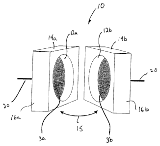
With reference to Figures 1 and 2, a first embodiment of a micro neutron
detector according to the invention is given generically as element 10.
Broadly
stated, the detector includes: a pocket, with gas; a neutron reactive
material;
and means for electrically biasing the pocket and neutron reactive material.
In
this manner, when introduced in a neutron environment (given generically as
neutron 5), neutron interactions in the neutron reactive material 3 cause
charged particles (reaction product) to eject in opposite directions 7, 9.
When
these energetic ionizing particles enter the pocket 11 filled with gas 8, they
produce ionization in the form of electron-ion pairs 13. In turn, the applied
voltage causes the positive ions and the electrons to separate and drift
apart,
electrons (-) to the anode and positive ions (+) to the cathode. The motion of
the charges then produces an induced current that is sensed and measurable
(e.g., signal), thereby indicating the interaction of neutron(s) in the
detector.
Electrical leads 20 provide the means to apply voltage to the detector and
also
extract the electronic signal from the detector.
17
CA 02574835 2007-01-22
WO 2006/110159 PCT/US2005/026840
With more specificity, Figure 1 shows an unassembled detector 10 in
two halves 14a, 14b that are brought together in the direction of bi-
directional
arrow 15, e.g., clamshelled, to form a pocket 11 in Figure 2. The pocket 11 is
defined by openings 12a, 12b in a housing 16a, 16b that embody the two
halves. In a preferred instance of manufacturing, the housing is void of
neutron-reactive or neutron-absorbing material and includes insulators, such
as
ceramics, aluminum oxide or oxidized silicon, and the openings 12a, 12b are
formed by cutting or etching a hole therein. Resulting volume size of the
pocket preferably includes anything on the order of less than about 1200 mm3.
More preferably, the volume ranges from a few cubic micrometers to about less
than 10 mm3 with a presently implemented design being about 0.39 mm3. With
this in mind, a pocket having a cylindrical shape, as shown, has a preferred
radius in each of the openings 12a, 12b of less than about 2 mm while a
thickness tl of the pocket 11 is less than about 2 mm. Of course, any sizes
are
possible as are any shapes of the pocket. Examples of this will be seen and
described relative to other figures.
Forming a portion of the pocket, and constructed to be in contact with
the gas 8 during use, is a neutron reactive material 3. In a preferred
embodiment, the neutron reactive material is a layer of about one micrometer
thick, t2, and embodies either a fissionable, fertile or a fissile material.
In this
regard, representative compositions include 235U, 238U, 233U, 232.hh, 239Pu,
2aiPu'
10 B, 6Li and 6LiF, for example. In other embodiments, the neutron reactive
material typifies a combination of the fissionable, fertile and fissile
materials.
In general, however, the line between fissionable, fertile and fissile
materials is
drawn, according to the invention, as: fissionable materials are materials
that
fission upon the absorption of a neutron with energy greater than the fission
18
CA 02574835 2007-01-22
WO 2006/110159 PCT/US2005/026840
critical energy which consist of, but are not limited to, 238U and 232Th;
fertile
materials are materials that become either fissile or fissionable materials
upon
the absorption of a neutron which consist of, but are not limited to, 238U;
and
fissile materials are materials that fission upon the absorption of a zero
energy
neutron and consist of, but are not limited to, 235U; 233U; 239Pu; and 241Pu.
Naturally, skilled artisans can contemplate other materials. Further, control
of
the composition of the neutron reactive material and its thickness, leads to
tailoring of detector type and neutron detection efficiency. In general, thin
neutron reactive coatings lead to decreased neutron interaction rates while
thicker neutron reactive coatings lead to increased rates.
Methods of applying the neutron reactive material vary. In the past, the
layer was deposited through a process in which uranyl-nitrate was coated onto
the conductive layer and then allowed to dry. The currently preferred method
of application involves electroplating the detector within an electrochemical
bath. In one instance, a solution of uranyl-nitrate or thorium nitrate covers
that
area of the detector needing coating. The detector then connects to a negative
terminal of an external voltage supply (not shown). As a result, the
positively
charged uranium based ions attract to the negatively charged device, forming a
thin layer of the neutron reactive material. However, other contemplated
methods of applying the reactive material include well known thin film or
other
deposition techniques, such as chemical vapor deposition, physical vapor
deposition (e.g., evaporation), sputtering, direct coating (such as painting
with
a brush or allowing a drop of diluted solution to dry on a surface). Further,
the
geometric shapes of the contacts and neutron reactive materials may be defined
with deep or regular reactive ion etching, photolithography, electron-beam
evaporation and lift-off techniques or the like.
19
CA 02574835 2007-01-22
WO 2006/110159 PCT/US2005/026840
Regardless of formation, skilled artisans will observe that the neutron
reactive material in the figures embodies two layers or sections 3a and 3b on
either sides of the pocket. However, the invention alternatively embraces only
a single instance of the neutron reactive material on a single side of the
pocket
and may exist as either 3a on the left or 3b on the right. Still further,
other
embodiments appreciate the shape of the pocket will vary as regular or
irregular shapes/surfaces and the neutron reactive material need only be
applied
with sufficient volume and position to cause the aforementioned interaction of
neutrons to occur upon the application of an electrical bias.
On a surface 23 of the neutron reactive material, and on a surface 25 of
the housing 16a, 16b, for example, a conductive material 27a, 27b, resides
having a thickness t3 of about one micrometer. In one aspect, the conductive
material includes any conductor including, but not limited to, copper, gold,
silver, aluminum, titanium, nickel, zinc, platinum, palladium, etc. In other
aspects, the conductor is a composition of conductors and/or other materials.
In a preferred embodiment, the material is a mixture of Ti/Au having
respective
concentration amounts of about 10% and 90%, or Ti/Pt having respective
concentration amounts of about 10% and 90%. Similar to the neutron reactive
material, the conductive material can be applied via a variety of mechanisms
and include those previously mentioned.
Connected to the conductive material through a hole in the housing are
electrical leads 20. In this manner, the aforementioned electrical bias of the
pocket and neutron reactive material can be applied. In a preferred
embodiment, the electrical leads include pure or combinations of conductors as
mentioned relative to the conductive material. In thickness, the cross-section
of the leads varies and is sufficient to apply a voltage bias to the neutron
CA 02574835 2007-01-22
WO 2006/110159 PCT/US2005/026840
reactive material and pocket in a range from about 1 volt to about 1000 volts.
Naturally, a sealant 17b fills the hole in the housing to seal the pocket I 1
from
gas leaks and secure the electrical leads in place. Optionally, this same
sealant
or another 17a also exists between the two halves of the housing to adhere the
halves together and seal the pocket shut from ambient conditions. Although
not preferred, mechanical fasteners could further be used in this regard. In
either, the structures need to be able to withstand relatively high
temperatures
as they will be exposed to the hostile environment of a nuclear reactor.
The gas 8 of the pocket 11 preferably includes one of argon, P-10, 3He,
BF3, and mixtures of Ar, He, BF3, C02, Xe, C4HIo, CH4, C2H6, CF4, C3H8,
dimethyl ether, C3H6 or C3H8. It may be pressurized too if desired.
Pressurizing, or not, like increasing or decreasing neutron reactive material
thicknesses, leads to tailoring of neutron detection efficiency. In general,
low
pressure gas leads to smaller signals, while higher pressure gas leads to
larger
signals, with a typical range of possible gas pressures ranging from about 0.1
atm to about 10 atm. Introduction of the gas to the pocket may occur in a
variety of ways. In one instance, gas fills the pocket simply by constructing
the
detector and sealing it in a gas environment, such as under a gas hood (not
shown). In another, gas is supplied via external sources and will be described
below. In still another, gas may represent the ambient air and exists in the
pocket simply by constructing the detector in other than a vacuum setting.
With reference to Figures 3-5, another embodiment of the invention
includes a micro neutron detector given generically as 30. In this design, a
plurality of substrates or insulator supports 32a, 32b, 32c are fastened
together
in the direction of arrows 34, 36, e.g., sandwiched, to form a pocket 38
filled
with gas 40. In one aspect, an opening 41 or hole is milled, etched or
otherwise
21
CA 02574835 2007-01-22
WO 2006/110159 PCT/US2005/026840
cut into an interior support 32b and when closed or sandwiched by exterior
supports 32a, 32c, the pocket is fully defined. The supports themselves may
embody any material so long as they are non neutron absorbing or reacting.
Preferred supports include alumina but could also embody a glassified
semiconductor substrate, such as oxidized silicon. As before, resulting pocket
volumes of the invention range from a few cubic micrometers to less than
about 1200 mm3 and are of any shape. A neutron reactive material exists in
contact with the gas and forms a portion of the pocket on either or both sides
at
positions 42a, 42b. Contacting the neutron reactive material and the exterior
supports, is a conductive material 44a, 44b for obtaining detector signals and
applying an electrical bias across the pocket and neutron reactive material
via
the functionality of electrical leads 46. A sealant 48 is also used in this
design
to seal the pocket from gas leaks, connect the supports 32 together and
support
the leads. Naturally, the leads could also contact the conductive material in
the
same fashion as previously described (e.g., through a hole in an exterior
support). Construction of this device could also occur in a gas environment as
previously described to fill the pocket 38.
Also, the in use application of neutron detection occurs as previously
described in a neutron environment 5, with reaction products occurring in
directions 7, 9 upon neutron contact with the neutron reactive material 42. In
turn, when these energetic ionizing particles enter the pocket 38 filled with
gas
40, they produce ionization in the form of electron-ion pairs 13. The applied
voltage then causes the positive ions and the electrons to separate and drift
apart, electrons (-) to the anode and positive ions (+) to the cathode. The
motion of the charges then produces an induced current that is sensed and
measurable (e.g., signal), thereby indicating the interaction of neutron(s) in
the
22
CA 02574835 2007-01-22
WO 2006/110159 PCT/US2005/026840
detector.
With reference to Figures 6a, 6b, 7a and 7b, an array 60 of a plurality of
micro neutron devices can be made together on a plurality of substrates or
supports 62a, 62b, 62c. Similar to Figures 3-5, an interior support 62b has
openings 61 formed therein. Each of the exterior supports 62a, 62c has a
conductive coating 64a, 64b applied thereto. In turn, on either or both of the
conductive coatings 64a, 64b, although only depicted on 64b, lies a coating or
layer of a neutron reactive material 62. Then, when the supports are fastened
together in the direction of arrows 65, 67, e.g., sandwiched, a plurality of
pockets 68 with gas 69 results. A plurality of electrical leads 63 are
fashioned
(e.g., evaporated, deposited, etc.) on one or more of the supports 62 to
ultimately supply/obtain signals from the detectors. In turn, conductors 71,
connected to external electronics, for example, (not shown) contact the leads
63. Optionally, one or more protective sleeves 75, 77 are provided. In one
embodiment, sleeve 75 is a hollow support rod providing mechanical support
for the conductors 71. In another embodiment, sleeve 77 surrounds sleeve 75
to provide protection to the array before it is inserted into a nuclear
reactor
environment. Either or both of the sleeves preferably serve to shield the
array
from any electromagnetic interference that may occur during operation of the
reactor, thereby reducing electronic noise contributions to measurements of
the
detectors. Also, and with the previously described detectors, preferred pocket
68 volumes range from a few cubic micrometers to less than about 1200 mm3.
Gas is introduced via construction of the array in a gas environment and
various thin film and/or VLSI technologies contribute to providing the
openings 61, the neutron reactive materials 62 and/or the conductive materials
64a, 64b on or in the various supports 62. Use of each individual detector
23
CA 02574835 2007-01-22
WO 2006/110159 PCT/US2005/026840
occurs as previously described. Preferred spacing S between adjacent pockets
preferably exists on the order of about 10 cm. Alternatively, one or more of
the
neutron reactive materials for the many pockets are different from other
neutron reactive coatings. Still alternatively, to eliminate the requirement
of a
conductive material disposed on the exterior supports, it is contemplated that
the exterior supports could be made of conductive materials while the interior
support is exclusively an insulator. In this manner, the neutron reactive
materials can be directly applied to the external supports and various
manufacturing steps eliminated. It is likely though, additional insulation
would
be required to prevent shorting upon application of an electrical bias to the
pocket.
In Figure 8, a specialized array 80 of a plurality of detectors includes the
instance of one or more of a triad 82 of pockets defined by openings 82a, 82b,
and 82c in an interior support 62b. In turn, a separate neutron reactive
material
is applied to one or both of the exterior supports 62a, 62c, although only
shown
on exterior support 62c, for two of the three pockets of each triad 82. For
example, on exterior support 62c, a first neutron reactive material 84a is
applied that corresponds to the pocket eventually formed by opening 82a upon
sandwiching/fastening the three supports 62a, 62b, and 62c together. A second
neutron reactive material 84b, different from the first, is applied that
corresponds to the pocket eventually formed by opening 82b upon fastening
together the three supports 62a, 62b and 62c. In a preferred embodiment, the
first neutron reactive material is 232Th while the second is 93%, 235 U. At a
position 84c that corresponds to the pocket eventually formed by opening 82c
upon fastening the three supports, there is no neutron reactive coating. In
this
manner each pocket of a triad 82 of the invention can provide readings
24
CA 02574835 2007-01-22
WO 2006/110159 PCT/US2005/026840
different from one another to create a multi-function detector. As presently
contemplated, the pockets arranged thusly enable the simultaneous detection of
fast and thermal neutrons, according to those pockets with neutron reactive
materials, while the no neutron reactive material pocket embodies an "empty
spot" enabling background subtraction and/or baseline readings. Further, the
neutron reactive materials 84d and 84e, for the second triad 82' of pockets
formed via openings 82a', 82b' and 82c' upon fastening the three supports,
respectively correspond to the neutron reactive materials 84a and 84b, thereby
adding redundancy, or are completely separate or different neutron reactive
materials thereby adding detection robustness. Naturally, gas (not shown)
fills
each of the pockets and contacts the neutron reactive materials, and
conductive
materials (not shown) underlie the neutron reactive materials for creating
electrical biases across the pocket and neutron reactive materials, during
use.
Also not shown, but skilled artisans will appreciate they exist, are various
electrical leads similar to the previous embodiments.
In still another embodiment, the empty spot shown does not need to
necessarily occur in the same position (e.g., corresponding to opening 82c or
82c') for each triad and one or both of the positions of the neutron reactive
materials can be interchanged. For example, the empty spot 84c could be
positioned where neutron reactive material 84a is located. In turn, neutron
reactive material 84a could be located at the position where neutron reactive
material 84b is located. Then, neutron reactive material 84b would be located
at the position of the empty spot at 84c. Of course, other positioning is
contemplated and embraced by the invention. Still further, the triads 82 shown
are arranged essentially in the shape of an equilateral triangle. Other
embodiments, however, contemplate other triangular relationships. In all
CA 02574835 2007-01-22
WO 2006/110159 PCT/US2005/026840
embodiments, however, vertical separation distances D, from one triad to
another, are preferably on the order of about 10 cm. On the other hand, an
internal separation distance, such as indicated by distance dl, of one opening
in
a triad to another in the same triad preferably exists on the order of about 1
mm.
Appreciating that over time, especially after long exposures of the
neutron reactive materials to radiation, the gas in the pockets of the micro
neutron detectors may become less effective. Thus, Figures 9-12 further
contemplate a detector design 100 including gas storage chambers 102 that
assist to replenish the gas in pockets. Similar to prior designs, a plurality
of
substrates or supports 91 and 93 are designed to be fastened/sandwiched
together. Namely, two supports 91 fasten on either sides 95, 97 of support 93.
In turn, because of the patterning of various holes or openings, one or more
pockets become defined at openings 104, 106 and 108 in the support 93. At
corresponding positions labeled X on support 91, neutron reactive materials
and conductive materials are coated, such as previously described. Then, when
the two supports 91 and support 93 are fastened together, the pockets include
corresponding neutron reactive materials on one or both sides of the pockets
as
well as a conductive material for use in creating an electrical bias across
the
pocket and neutron reactive material. Further, because the positions labeled Y
on the supports 91 have no openings, upon fastening the supports together, gas
storage chambers result at 102. Then, during use as gas in the pockets
depletes,
the gas in gas storage chambers 102 replenishes them. In this regard, gas
diffusion channels 110 lead from the gas storage chambers to the pockets. Gas
fill channels 114, as their name implies, also enable the filling of gas into
the
gas storage chamber during manufacture.
26
CA 02574835 2007-01-22
WO 2006/110159 PCT/US2005/026840
Also, because the design shown further contemplates a triad of pockets
in a detector array for simultaneously detecting fast and thermal neutrons as
well as providing a background or baseline reading, for example, two of the
pockets preferably have different neutron reactive materials coated at any of
the
two positions labeled X while the third remaining position label X has no
neutron reactive material. In this manner, the functionality of the design of
Figure 8 is further achieved, if desired.
To further facilitate construction of the detector, the supports have
additional holes and/or channels. Namely, support 93 contemplates a variety of
epoxy channels 112 that become filled with epoxy or other adhesives to assist
in fastening the supports together. All supports 91 and 93 also include a
variety of wire feed through holes 90 (only a few are labeled in each figure)
to
facilitate the interconnection of electrical leads into contact with the
conductive
material. A thermocouple hole 96 is provided to facilitate connections of the
detector design 100 to an external environmental monitor, such as a
thermocouple (not shown). Support 91, on the other hand, also has a variety of
wire solder points 94 formed namely as indentations in a surface of the
support.
As skilled artisans will appreciate, the supports 91, 93 can be mass-
produced using common thin film and very large scale integration (VLSI)
processing techniques. For instance, the patterning of holes, indentions or
other can be etched entirely through supports embodied as common silicon
wafers or alumina, for example. Naturally, the design and placement of these
holes have an effect on the efficiency and efficacy of the process itself;
and,
many possibilities exist for the design of supports.
F,XAMPi.F.
27
CA 02574835 2007-01-22
WO 2006/110159 PCT/US2005/026840
Prototype micro neutron detectors were manufactured from machined
aluminum oxide (alumina) pieces, and each detector was embodied as a
plurality of three fastened supports, such as representatively shown in
Figures
3-5. The interior support included an opening that, when fastened to the
exterior supports, defined a generally cylindrical gas pocket having a 2-mm
diameter and 1-mm thickness. To make the detector, compositions of Ti/Au
were evaporated on each of the exterior supports to form an alumina cathode
and anode. In turn, the support having the cathode was aligned and fastened to
the interior support with an epoxy. A dilute solution of Uranyl-Nitrate
(neutron
reactive material) was then applied over the Ti/Au forming the cathode and
baked with an infrared lamp for 5 minutes. Afterwards, the fastened interior
support and the exterior support forming the cathode, including the baked
uranyl-nitrate, were inserted into a glove box, of sorts, which was backfilled
with P-10 gas. After waiting a sufficient amount of time for the gas to
displace
any residual air in the glove box, the other exterior support, forming the
anode,
was fastened with epoxy, thereby trapping the P-10 gas inside the pocket.
Thereafter, the entirety of the detector was cured for 24 hours at 200 F in a
baking oven. Later, multiple other detectors were made according to this
recipe.
For initial testing, the prototype micro neutron detectors were introduced
into a neutron environment embodied at a thermal neutron beam port 190
(Figure 20b) tangential to the Kansas State University (KSU) TRIGA Mark II
reactor core, seen in Figures 20b, 20c and 2d, to observe their spectral
characteristics and gamma ray insensitivity. Upon a bias of +200 volts across
the pocket and neutron reactive material, the detectors were tested at full
reactor power, which is known to provide (at the tangential beam port) a
28
CA 02574835 2007-01-22
WO 2006/110159 PCT/US2005/026840
thermal neutron flux of 1.6 x 10⁶ n-cm 2-s-1. Of this, the gamma ray component
is approximately 100 R per hour and spectra for the testing were accumulated
with and without a Cd shutter, thereby allowing for the observation of the
gamma ray contributions to the signal.
Appreciating that a neutron's angle of entry into a detector will change
the magnitude of the pulse (signal) returned from the detector, a Monte Carlo
code was written beforehand to model the expected pulse height distribution
from a given micro neutron detector. As seen in Figure 19b, the model
depicted the expected spectral features (in terms of Number of Paths versus
Path Length) for micro neutron detectors having a cylindrical pocket with both
a 3-mm diameter (R=1.5mm) and a thickness of 1-mm wide (H=lmm); and a
4-mm diameter (R=2mm) and a thickness of 2-mm wide (H=2mm). What
skilled artisans should appreciate is the salient energy peak predicted near
mid-
spectrum. For example, at path lengths of 1 and 2 mms, dramatic increases in
the number of paths are expected for each of the detectors. With more
specificity, the peaks indicate the average energy deposition in the detectors
occurring with reaction product trajectories approximately perpendicular to
the
general length of the conductive and neutron reactive material (e.g., Figures
2
and 4), whereas the continua are from other possible angular trajectories
(e.g.,
reference arrows 7 and 9 of Figures 2 and 4).
As was hoped for, Figure 19a shows an actual fission product spectrum
obtained from reading output signals of an actually tested micro neutron
detector and such compares favorably to the predicted response modeled in
Figure 19b. Namely, both graphs show little or no detection at low spectrum
(e.g., low Channel Number or Path Length) a sharp increase to a peak, which
thereafter quickly tapers to little or no detection (e.g., at relatively high
Channel
29
CA 02574835 2007-01-22
WO 2006/110159 PCT/US2005/026840
Number or Path Length). Thus, the initial viability and usefulness of the
micro
neutron detectors were fairly proven. Also, further tests with cadmium
shielding pieces between the neutron source and the micro neutron detectors
showed almost no pulses from the gamma rays, demonstrating the detectors
also have an excellent n/y detection ratio.
Afterwards, testing of the micro neutron detectors moved from the
tangential beam port 190 to within the reactor core at 210 (Figure 20b), for
example. Within a 20 ft long aluminum sampling tube or sleeve, the micro
neutron detectors were placed within the core of the KSU TRIGA Mark.Il
nuclear reactor at positions labeled central thimble (CT) or flux probe hole
(=)
(Figure 20d), for example. Connecting wires extending from the reactor core,
up through the aluminum tube and at out of the top 200 (Figure 20b) of the
reactor pool, were used to connect the detectors to a commercial Ortec 142A
preamplifier, thereby ensuring that the signal reading electronics (not shown)
were not in a hanmful radiation field. Then, detector measurements of 15-
minute durations were taken with the reactor power incrementally changed in
power from 1 mW up to 200 kW, hence changing the thermal flux at the
detector location from 103 - 1012 n-cm 2-s 1. Further, the detector was
operated
in pulse mode for the entire experiment.
Representatively, Figure 13 shows a contemplative design of a relatively
lengthy detector assembly 125 for use in this regard. Specifically, the
assembly
125 includes a sleeve 126 having a terminally disposed detector cavity 127 for
positioning one or more of the described micro neutron detectors deep within a
relatively tall nuclear reactor. At 129, an index stop exists to prevent the
assembly from traveling too deep within the reactor and/or maintain the
detectors at a predetermined height. Naturally, the stop is contemplated as
CA 02574835 2007-01-22
WO 2006/110159 PCT/US2005/026840
adjustable. At 130, the preamplifier (of the type mentioned, for instance)
exists
to boost signals coming from the detectors. The preamplifier also exists at a
sufficiently safe distance from a core in which it is used. At 132,
pluralities of
electrical leads exist to ultimately connect the detectors to external
electronics
(not shown) for actually reading the detector signals. Ultimately, noise
contributions from coupling capacitance can be reduced, while minimizing
radiation damage to the electronics. The entire assembly is leak proof and
waterproof. Preferred structural exteriors include aluminum.
Returning to the Example, Figure 20a plots the observed results of the
micro neutron detector(s) as Count Rate versus Reactor Power. As stated, the
KSU TRIGA Reactor was operated from low power up to 200 kW, changing in
fifteen-minute intervals. Unexpectedly and advantageously, the linearity of
the
graph (especially between reactor powers of 1 Watt to greater than 105 Watts)
shows that the neutron reactive material of the detectors does not degrade at
higher reactor powers. Heretofore, no other detectors have achieved responses
of the type indicated. Further, it is expected that if a nuclear reactor could
be
tested having power greater than 105 Watts, the linearity of the detector
response would continue. Unfortunately, for reactor powers below 1 Watt, the
KSU TRIGA reactor cannot be regulated accurately enough and the graph
linearity breaks down. However, it is expected that if it could be better
controlled, the graph linearity would also continue for low powers.
Advantageously, the tested micro neutron detectors emitted readings nearly
instantaneously. Conventional gas-filled detectors, on the other hand, are of
larger volume than the described invention, and the time it takes to form the
2 5 signal from the device can take several hundred microseconds to several
milliseconds. Under high count rate conditions, conventional detectors also do
31
CA 02574835 2007-01-22
WO 2006/110159 PCT/US2005/026840
not have enough time to distinguish between separate neuron interaction
events, hence the signal pulses collide, or pile-up, which causes the readout
electronics to miss events, wherein the time duration of these missed events
is
referred to as dead-time. However, the described invention is much smaller,
being a micro neutron detector, and does not suffer the dead time problem as
do their conventional counterparts. This substantially reduced dead-time
amounts to a further significant advancement over the prior art, in which
present day, conventional detectors are unable to measure a count rate above
104 counts per second (cps) without substantial dead time or rollover.
Moreover, the lack of dead time in the instant invention eliminates both the
need to calibrate the timing of the detector signals and the need to use a
correlation chart, as is often presently done.
As a result, the EXAMPLE clearly shows capability of measuring
i
thermal neutron fluxes in micro neutron detectors ranging from 103-1012 n-cm
2-s-1 with no sign of dead time losses. To date, further testing has revealed
micro neutron detectors withstanding neutron fluences exceeding 10 19 n-cm'2
without any noticeable degradation. The count rate observed, however, is still
below the theoretical maximum; hence, the detectors are expected to operate,
still in pulse mode, within the higher neutron fluxes of power and naval
reactors.
As further advantage, since the charge-detecting medium of the
detectors is a gas, it is improbable that gamma rays will ever interact
therein;
hence, the micro neutron detectors of the instant invention naturally
discriminate out gamma-ray background noise. Furthermore, since the device
is gas-filled, there is no detecting medium that radiation can actually
destroy.
This too is a clear advantage over prior art liquid or solid detectors. The
32
CA 02574835 2007-01-22
WO 2006/110159 PCT/US2005/026840
detectors are also much more radiation hardened than typical semiconductor
and liquid-based neutron detectors as well.
With reference to Figures 21-30, other embodiments of micro neutron
detectors of the invention are given generically as 200. In one instance, they
include an array of a plurality of detectors. In another, they embody
pluralities
of pockets formed as adjacent capillary channels. During use, however, they
behave as the previously described embodiments. In a broad sense, the
detectors include: a pocket, with gas or a fluid; a neutron reactive material
forming a portion of the pocket and contacting the gas; and an electrical bias
across the pocket and neutron reactive material. In this manner, when
introduced in a neutron environment, neutron interactions in the neutron
reactive material cause charged particles (reaction product) to eject in
opposite
directions. When these energetic ionizing particles enter the pocket filled
with
gas or fluid, they produce ionization in the form of electron-ion pairs. In
turn,
the applied voltage (electrical bias) causes the positive ions and the
electrons to
separate and drift apart, electrons (-) to the anode and positive ions (+) to
the
cathode. The motion of the charges then produces an induced current that is
sensed and measurable (e.g., signal), thereby indicating the interaction of
neutron(s) in the detector. A conductive material provides the means to get
the
signal from the detector.
With more specificity, Figures 21 and 22 show a plurality of detectors
200. In general, first and second supports or substrates 202, 204 are
fabricated
with corresponding features or surfaces, such that upon their fastening
together,
pluralities of pockets 206, in the form of channels, result. In one instance,
the
supports or substrates embody semiconductor or silicon wafers readily and
easily fabricated via thin film and VLSI techniques. In another, they embody
33
CA 02574835 2007-01-22
WO 2006/110159 PCT/US2005/026840
alumina and are readily and easily fabricated with laser ablation, for
example.
Still other supports contemplated include the insulators previously described.
In either, a neutron reactive material 208 is a feature of the support and
forms a portion of each pocket 206 on either or both sides, such as at both
positions 208a and 208b or at either one of the positions 208a or 208b.
Candidate neutron reactive materials have already been recited and similar or
different materials can be used for each pocket 206-1, 206-2, 206-3, etc. to
create similar detectors or simultaneously a fast and thermal neutron detector
(including or not a pocket 206 with no neutron reactive material to obtain a
baseline or background reading as previously discussed). A conductive
material 210 contacts the neutron reactive material and is used to obtain the
signals of the detectors and apply an electrical bias to the pocket.
Naturally, if
the neutron reactive material 208 only existed at either one of positions 208a
or
208b, the conductive material itself would further exist in direct contact
with
the gas in the pocket (not shown).
In one manufacturing embodiment, the conductive material is positioned
by forming a via-hole in the supports 202, 204 and then filling the hole with
a
conductor. Candidate conductors have, of course, already been recited. Once
formed, the neutron reactive material is then patterned on top of the
conductor.
Skilled artisans will appreciate that fabrication of these supports will
likely
occur with an orientation perpendicular to that shown in Figures 21 and 22,
such that a neutron reactive material existing on 'top' of the conductor
relates
to the well known practice of fabricating substrates on a top surface of an
underlying surface. Representatively, this is seen in Figure 30, for example
in
which a support, e.g., 270, 290, undergoes fabrication through steps (1), (2),
(3)
and (4). More on this will be described below.
34
CA 02574835 2007-01-22
WO 2006/110159 PCT/US2005/026840
During use, referring back to Figure 21 and 22, the detectors exist in a
neutron environment, labeled "neutrons." As neutron interactions in the
neutron reactive material 208a occurs, charged particles are caused to eject
in
opposite directions (although only direction 209 is shown). When these
energetic ionizing particles (reaction product) leave the neutron reactive
material and enter the pocket 206 filled with gas or fluid, they produce
ionization in the form of electron-ion pairs 213. In turn, and appreciating an
electrical bias, in the form of a voltage across the pocket and neutron
reactive
material exists via the conductor material 210a, 210b, the positive ions and
the
electrons to separate and drift apart, electrons (-) to the anode and positive
ions
(+) to the cathode. The motion of the charges then produces an induced current
that is sensed and measurable (e.g., signal), thereby indicating the
interaction of
neutron(s) in the detector 200.
-
With reference to Figure 23, and appreciating the support 202 exists in
three-dimensions, vice the two dimensions shown in Figures 21 and 22, each
pocket 206 resides longitudinally along the support in the direction of bi-
directional arrow A. Representative volumes of these pockets also preferably
range from a few cubic micrometers to less than 1200 mm3. In length
(direction of arrow A and x-axis), they will average about 20 cm, more or
less.
In depth (y-axis), they will be about 1 mm. In the direction of the z-axis,
each
channel will be about 1 mm. Also, because the conductor material, also
referred to in this view as contacts, preferably is formed in via-holes in the
support, pluralities of the contacts 210 can exist in the directions of arrow
A in
a single pocket or channel especially labeled 215, for example. In turn,
because each channel 215, 217, 219, 221, 223 has pluralities of such contacts,
signal outputs can be obtained at each individual contact thereby lending the
CA 02574835 2007-01-22
WO 2006/110159 PCT/US2005/026840
development of an X-Y-Z axis map of neutron fluxes for any given neutron
environment in which a single detector array 200 is placed. Further, with the
addition of multiple arrays of such detectors placed throughout a nuclear
reactor, for example, a comprehensive X-Y-Z map can be made for the entirety
of the reactor. Although X-Y-Z mapping can also occur by positioning
pluralities of the individual detectors previously mentioned (e.g., Figures 1-
5)
comprehensively throughout a reactor, this embodiment would naturally be
able to accomplish it with fewer overall detector housings.
With reference to Figure 25, a three-dimensional view of an entirely
assembled array of detectors 200 is seen, especially the feature of a
conductor
material 210 existing in an entirety of a via-hole 220 etched, for example, in
a
support 204. Further, the conductor material of this or other embodiments may
separately and distinctly include a contact. Representative materials for the
contact especially include, but are not required to be, any of Ti, Au, Pt or
Pd.
Further, this embodiment especially contemplates that gas in the pockets
206 may be flowed along the length of any given channel in the direction(s) of
arrow A, for example. As presently depicted, gas will flow in the channel in
the direction of arrow IN and will flow out in the direction of arrow OUT. In
a
preferred embodiment, gas flow rates on the order of standard cubic feet per
hour (scfh) are contemplated. Gas compositions are of those already described.
In alternate designs, each individual channel could have its gas flow IN and
OUT reversed from that shown. Still alternatively, gas can be substantially
permanently sealed in the pockets, not flowed, as with some of the previous
embodiments and can be done in the manners described in a gas environment,
for example.
With reference to Figures 24a and 24b, a planar view of a cross-section
36
CA 02574835 2007-01-22
WO 2006/110159 PCT/US2005/026840
of the pockets or channels (oddly numbered from 215 - 245 in the views) and
their gas flow directions is seen. Individual conductor materials 210 in
adjacent channels, however, align with one another in the X-direction in
Figure
24a, but not in Figure 24b. In one instance, adjacent channels are separated
by
a distance D3 of about 3 mm. In another, adjacent channels are separated by a
distance D4 of about 2 mm. In the X-direction, conductor materials 240, 242
are separated by a distance D5 of about 3 mm. While a stagger or pitch P
between conductor materials 241, 243 exists on the order of about 2 mm. Of
course, other arrangements of conductor materials are contemplated and
embraced herein.
With reference to Figure 29, completely assembled supports 202, 204
could further be mounted, mechanically and electronically, onto substrates,
such as a printed circuit board (PCB) 250, to facilitate readout of the
signals of
any of the micro neutron detectors. In one instance, dedicated readout
connector ribbons 252, 254 could attach to the PCB 250 and relate respectively
to the signals from the conductor materials arranged in the X and Y directions
of Figures 24, for example. Further, externally supplied gas could be flowed
through pockets 206 via connections 260, 262. As shown, gas is supplied into
the pockets from two directions (e.g., 260 and 262). Thus, gas out could exit
from side 264. Alternatively, either of connections 260 or 262 could be
configured such that one supplies gas in and one receives gas out. Skilled
artisans can, of course, contemplate other examples.
With reference to Figures 26-28, alternate fabrication of a plurality of
micro neutron detectors formed with supports having channels as pockets is
contemplated. For example, figure 26 shows a support 202 as already
described. However, support 270 is essentially flat on a surface 271 and
strips
37
CA 02574835 2007-01-22
WO 2006/110159 PCT/US2005/026840
of materials 272, 274 are fabricated, through techniques previously mentioned,
to represent rows of contacts 272 and rows of neutron reactive materials. In
this manner, only one substrate, e.g., 202, needs to have a channel 215, 217,
219, 221, 223 fashioned therein. In turn, this facilitates ease of
manufacturing.
In Figure 27, support 202 is fastened with support 280 to form a
plurality of micro neutron detectors. However, support 280, instead of having
strips of materials for contacts and neutron reactive materials, has a
substantial
entirety of its surface 281 coated with, first, a conductor material for the
contacts and, second, with a neutron reactive material. In this fashion, no
patterning, etching, etc., need occur with the support 280 and further eases
manufacturing constraints.
In Figure 28, support 202 is fastened with support 290. In this instance,
support 290 has strips of materials to form contacts 292 and neutron reactive
materials 294, however, these strips are oriented perpendicularly to those of
Figure 26. In this fashion, readout of the detected neutrons, for example,
reveals precise locations by appreciating anodes, for example, exist with
support 202 and cathodes with support 290. As a result, the location of
neutron
interaction events can be determined as a function of the nearest intersection
point of channels from which the signals are extracted.
With reference to Figure 30, processing steps on a support 270, 290 to
receive strips of materials is seen diagranunatically as (1), (2), (3) and
(4).
Shown (1) is a possible method by which to fabricate one side 291 of the
channel detector, in which a substrate 290 is ablated with a laser 293 to form
grooves entirely through the material. Afterwards, (2) the grooved substrate
295 is attached to a second substrate 270 upon which metallic strips are
coated
with neutron reactive material. The grooves 297a are aligned with the metallic
38
CA 02574835 2007-01-22
WO 2006/110159 PCT/US2005/026840
strips 297b. The (3) excess material from the grooved substrate is cut at 299
from the configuration, leaving (4) a prepared single side of a channeled or
capillary detector 301.
In either of the embodiments of Figures 21-30, for example, it is
expected that an increase in the number of preamplifiers would be required to
boost signals levels, leading to external electronics, compared to other
designs.
Nonetheless, these designs will offer a high spatial resolution detector that
is
significantly more radiation hard than semiconductor counterparts. They are
also expected to be used at facilities where neutron measurements are
important in the energy range usually characterized by cold to epi-thermal
neutrons. High density polyethelene (HDPE) plates in front of sections of the
detector (not shown) can further be used to thermalize fast neutrons and
provide some energy information on the incident neutron field. Selectively
chosen collimator holes (not shown) in the HDPE can assist with directional
sensitivity. Any of the supports, especially if embodied as semiconductor or
silicon wafer, may additionally have an oxide layer grown over an entirety
thereof to serve as insulation.
With reference to Figure 31, skilled artisans will appreciate the response
of the neutron reactive material of the inventive micro neutron detectors will
change over time. In this regard, the lifetime reaction rate of various
nuetron
reactive materials are given. Also, great differences in reaction rates are
seen
between 235U and 232Th in early stages of their respective lives. Thus, this
is
one reason for selecting these two materials to play a respective role in a
micron neutron detector embodied as a triad for simultaneously detecting both
fast and thermal neutrons. Namely, highly enriched 235U will have a
principally
thermal neutron response while detectors coated with 232Th will have a fast
39
CA 02574835 2007-01-22
WO 2006/110159 PCT/US2005/026840
neutron response. Additionally, knowledge of any given reactor's energy
dependent neutron flux profile allows for a detector's lifetime optimization,
including a flatter neutron response. For example, the KSU TRIGA Mark-II
nuclear reactor may operate at a constant steady state power of 250 kW. As
can be seen in the graph, one percent signal change in this reactor under such
conditions for natural uranium would be reached in only 0.268 years, 0.038
years for 93 wt% enriched 235U, and less than 1 week for 232 Th. However, by
using a 60/40 mixture of 1.1843 wt% enriched 235U and 232Th, the lifetime can
be extended to 57.59 years for 1% signal change. A 5% signal change, on the
other hand, would occur in 87.72 years while a 25% signal change in 237 years.
Thus the coatings may be tailored for each detector's use and to provide
specific neutron energy information.
With reference to Figure 32, the background insensitivity of a
representative micro neutron detector of the invention is seen. Namely, a
graphical analysis appears for gamma-ray energy deposition in 500 microns of
1 atm argon fill gas (very similar to P-10 gas) for various gamma-ray
origination energies. Applying a curve fit to this data, along with the
assumption that the maximum energy deposition cannot exceed the origination
energy of the gamma-ray, it is obtained that the greatest energy will be
departed
by a 1 keV gamma-ray and will deposit only 658 eV. This is insignificant and
easily discriminated out when compared to the 3 MeV signals from fission
products.
With reference to other graphs, the energy deposition and ranges of ' B
reaction products in 1 atm of P-10 gas are shown in Figs. 14 and 15. Clearly,
only a fraction of energy will be deposited within a two-mm wide cavity of P-
10 gas. However, from Fig. 15, the average energy deposited from the 1.47-
CA 02574835 2007-01-22
WO 2006/110159 PCT/US2005/026840
MeV alpha particle will be 0.02 eV/angstrom, which is approximately 400 keV
for a 2-mm wide cavity. The 840-keV Li ion deposits more energy, averaging
approximately 500 keV for a 2-mm wide cavity. Figure 16 shows a thermal
neutron reaction product spectrum taken with a prototype 10B-coated MPFD.
Designed and constructed by the inventors, the device was manufactured with a
1-micron 10B coating atop aluminum oxide walls and had a 2.5-mm diameter
gas pocket that was 2 mm wide. Two spectra are shown: one with 20 volts bias
and the other with 250 volts bias. When biased at 20 volts, the integrated
counts yielded 1.1 % neutron detection efficiency, and when biased to 250
volts
yielded 2% thermal neutron detection efficiency. The total count rate
increased
up to a bias of 100 volts, after which the count rate stabilized. This
important
result demonstrates that the proposed device is viable and can be operated at
modest voltages.
For micro neutron detectors with 235U as the reactive film, Figs. 17 and
18 show the ranges and energy deposition within 1 atm of P-10 gas for 95 MeV
bromine fission fragments and 60 MeV iodine fission fragments. It again
becomes obvious that the fission fragments will only deposit a small portion
of
energy within the pockets, yet from Fig. 18, the deposited energies will be
2.9
MeV for the bromine fragment and 3 MeV for the iodine fragment, all within a
pocket cavity only 500 microns wide (e.g. tl ). Energies of such large
magnitude will be easily discriminated from background gamma rays, and the
thinner gas pocket requires only 25 volts operating bias.
With reference to Figure 33, any one or more micro neutron detectors of
the invention can be associated with and remain with a fuel bundle for times
of
use in nuclear reactors and later after fuel bundle burn-up. In this manner,
upon inserting the fuel into the reactor, detectors are also inserted and
provide
41
CA 02574835 2007-01-22
WO 2006/110159 PCT/US2005/026840
an instantaneous in-core neutron flux measurement capability. During use, this
also adds to reactor fuel efficiency increases because real-time adjustments
of
fuel bundle location or locating spotty fuel bum-up, for example, can be made
based on the output readings of the detectors. Appreciating average fuel
bundles cost hundreds of thousands of dollars or more, the more effective
burning of fuel will certainly save money too. Further, upon removal of the
fuel bundle from the reactor, after use, the detectors can remain with the
bundle
and later provide an indication of the state of the bundles, such as
before/during
transportation to waste sites.
As is known, a fuel rod 300 is comprised of a plurality of fuel pellets
302. In turn, pluralities of fuel rods combine to form a fuel bundle 350. The
fuel bundle is then geometrically dispersed 360 in a reactor vessel 365 to
form
a reactor core 370. In one embodiment, dispersed amongst the pellets is one
or more micro neutron detectors 304, having pockets 308, of the type
previously described. In turn, electrical leads or wires 306 extend from the
detectors for obtaining detector signal readouts. In another, an instrument
rod
320 includes the one or more detectors and the rod itself is co-located with a
fuel bundle 350 and bound with a well-known fuel bundle support 355. Also,
the instrument rod may be of the type representatively seen in any of Figures
6,
7 and 13 and placement of the rod may also occur at various positions,
especially the flux probe hole position of Figure 20d. Figure 34, on the other
hand, serves to illustrate the concept of Figure 33 except for showing a
representatively cylindrical fuel bundle 358 that often typifies a CANDU fuel
bundle. In either, the fuel bundles 350, 358, are further disposed in a
moderator 380 of the nuclear reactor, representatively seen in Figure 20b.
Apart from the fuel bundles, skilled artisans will appreciate that
42
CA 02574835 2007-01-22
WO 2006/110159 PCT/US2005/026840
insertion of the micro neutron detectors of the invention are readily placed
in
the moderator 380 (Figure 20b) of a given nuclear reactor. In this regard,
dispersal in three-dimensions will readily lead to mapping an entirety of
neutron flux of a reactor.
For example, with or apart from the fuel bundles, Figure 35 shows
pluralities of micro neutron detectors, labeled X, inserted into a reactor
moderator 380. In one embodiment, it is anticipated to place forty-five to
fifty
such neutron detectors in the moderator in a vertical manner, such as on one
or
more rods 383 (shielded or not with sleeves previously described). In turn,
each detector exists at various heights in the moderator, such as
representatively seen by hl, h2, h3 for each of the micro neutron detectors C,
B
and A, respectively. Then, upon taking the readings/measurements of the
detectors, and appreciating that each rod 383 has a different X-Y position in
a
plane shown as 385, a three-dimensional map 390 of the neutron flux of the
reactor can be' obtained via correlation to each detector, such as the
detectors
labeled A, B and C.
The foregoing description is presented for purposes of illustration and
description of the various aspects of the invention. The descriptions are not
intended to be exhaustive or to limit the invention to the precise form
disclosed.
The embodiments described above were chosen to provide the best illustration
of the principles of the invention and its practical application to thereby
enable
one of ordinary skill in the art to utilize the invention in various
embodiments
and with various modifications as are suited to the particular use
contemplated.
All such modifications and variations are within the scope of the invention as
determined by the appended claims when interpreted in accordance with the
breadth to which they are fairly, legally and equitably entitled.
43