Note: Descriptions are shown in the official language in which they were submitted.
CA 02575174 2009-12-21
77496-228
FREQUENCY DIVIDER WITH VARIABLE CAPACITANCE
BACKGROUND
[0001] An Electronic Article Surveillance (EAS) system is designed to prevent
unauthorized removal of an item from a controlled area. A typical EAS system
may
comprise a monitoring system and one or more security tags. The monitoring
system
may create an interrogation zone at'an access point for the controlled area. A
security
tag may be fastened to an item, such as an article of clothing. If the tagged
item
enters the interrogation zone, an alarm may be triggered indicating
unauthorized
removal of the tagged item from the controlled area.
[0002] Some EAS systems may use a security tag having a frequency divider to
generate a signal in response to an interrogation signal. The stiucture of the
frequency divider may, however, contribute to a loss of energy that reduces
the
conversion efficiency of the frequency divider. Consequently, by increasing
the
efficiency of the frequency divider, performance of the EAS system may be
improved
and the cost of the EAS system may be reduced. Accordingly, there may be need
for
improved frequency dividers in EAS systems.
1
CA 02575174 2009-12-21
77496-228
SUMMARY OF THE INVENTION
In one broad aspect of the invention, there is provided a marker,
comprising: a first resonant circuit comprising a first planarized coil having
a pair
of terminals and a capacitor connected to said pair of terminals, said first
resonant
circuit to generate a first resonant signal in response to an interrogation
signal;
and a second resonant circuit comprising a second planarized coil having a
pair of
terminals and a variable capacitor connected to said pair of terminals, with a
portion of said second planarized coil to overlap a portion of said first
planarized
coil, said second resonant circuit to receive said first resonant signal and
generate
a second resonant signal having a second resonant frequency; wherein said
variable capacitor comprises a metal-oxide semiconductor device, said metal-
oxide semiconductor device to operate as a non-linear capacitor having varying
amounts of capacitance corresponding to varying amounts of voltage received by
said metal-oxide semiconductor device; and wherein said metal-oxide
semiconductor device comprises a lamination of an insulation material and a
semiconductor material disposed between metal terminals, and as said voltage
applied across said terminals varies, a concentration of charge carriers in a
region
of said semiconductor material adjacent to said insulation material also
varies to
thereby vary said capacitance.
In one broad aspect of the invention, there is provided a system,
comprising: a transmitter to transmit an interrogation signal operating at a
first
frequency; a security tag having a marker, said marker comprising: a first
resonant circuit comprising a first planarized coil having a pair of terminals
and a
capacitor connected to said pair of terminals, said first resonant circuit to
generate
a first resonant signal in response to said interrogation signal; a second
resonant
circuit comprising a second planarized coil having a pair of terminals and a
variable capacitor connected to said pair of terminals, with a portion of said
second planarized coil to overlap a portion of said first planarized coil,
said second
resonant circuit to receive said first resonant signal and generate a second
resonant signal having a second resonant frequency; wherein said variable
capacitor comprises a metal-oxide semiconductor device, said metal-oxide
semiconductor device to operate as a non-linear capacitor having varying
la
CA 02575174 2009-12-21
77496-228
amounts of capacitance corresponding to varying amounts of voltage received by
said metal-oxide semiconductor device; and a detector to detect said second
resonant signal from said marker and generate a detection signal in accordance
with said second resonant signal; wherein said metal-oxide semiconductor
device
comprises a lamination of an insulation material and a semiconductor material
disposed between metal terminals, and as said voltage applied across said
terminals varies, a concentration of charge carriers in a region of said
semiconductor material adjacent to said insulation material also varies to
thereby
vary said capacitance.
In one broad aspect of the invention, there is provided a method,
comprising: receiving an interrogation signal at a first resonant circuit for
a
marker; generating a first resonant signal having a first resonant frequency
in
response to the interrogation signal; receiving said first resonant signal at
a
second resonant circuit overlapping said first resonant circuit; and
generating a
second resonant signal having a second resonant frequency in response to said
first resonant signal using variable capacitance, with said second resonant
frequency being different from said first resonant frequency; wherein the
variable
capacitance is provided by a metal-oxide semiconductor device, the metal-oxide
semiconductor device comprising a lamination of an insulation material and a
semiconductor material disposed between metal terminals, and as a voltage
applied across the terminals varies, a concentration of charge carriers in a
region
of the semiconductor material adjacent to the insulation material also varies
to
thereby vary the capacitance.
lb
CA 02575174 2009-12-21
77496-228
BRIEF DESCRIPTION OF THE DRAWINGS
[0003] The subject matter regarded as the embodiments is particularly pointed
out
and distinctly claimed in the concluding portion of the specification. The
embodiments, however, both as to organization and method of operation,
together
with objects, features, and advantages thereof, may best be understood by
reference to
the following detailed description when read with the accompanying drawings in
which:
FIG. I illustrates an EAS system suitable for practicing one embodiment;
FIG. 2 illustrates a block diagram of a marker in accordance with one
embodiment;
FIG. 3 is a block flow diagram of the operations performed by a marker in
accordance with one embodiment;
FIG. 4 is a first circuit for implementing a marker in accordance with one
embodiment;
lc
CA 02575174 2007-01-24
WO 2006/049667 PCT/US2005/027995
FIG. 5A is a sectional view of a capacitance element without a voltage being
applied across the terminals in accordance with one embodiment;
FIG. 5B is a sectional view of a capacitance element when a voltage is applied
across the terminals in accordance with one embodiment;
FIG. 5C is a sectional view of a capacitance element when a voltage is applied
across the terminals in accordance with one embodiment;
FIG. 6 illustrates a graph of capacitance versus gate voltage in accordance
with one embodiment;
FIG. 7 illustrates a graph of the measured capacitance and dissipation data
(CV/DV) characteristics of a metal-oxide semiconductor (MOS) device in
accordance
with one embodiment;
FIG. 8 illustrates a graph of carrier concentration versus capacitance ratio
in
accordance with one embodiment; and
FIG. 9 is a second circuit for implementing a marker in accordance with one
embodiment.
DETAILED DESCRIPTION
[0004] The embodiments may be directed to an EAS system in general. More
particularly, the embodiments may be directed to a marker for an EAS security
tag.
The marker may comprise, for example, a frequency-division marker configured
to
receive input RF energy. The frequency-division marker may recondition the
received RF energy, and emit an output signal with a frequency that is less
than the
input RF energy. In one embodiment, for example, the output signal may have
half
the frequency of the input RF energy. This type of frequency-division marker
may be
suitable for use in low bandwidth environments, such as the 13.56 Megahertz
(MHz)
Industrial, Scientific and Medical (ISM) band.
[0005] Conventional EAS systems are unable to effectively operate in the 13.56
MHz ISM band. Conventional EAS systems typically use a marker consisting of a
single inductor-capacitor (LC) combination resonant circuit configured to
resonate at
a predetermined frequency. Due to the high operating frequency of the 13.56
MHz
ISM band, such a marker may require an inductor with a few turns, and a
capacitor
ranging between 10-100 pico-farads (pF). Detecting such a single-resonance
marker,
however, may require a relatively complicated detection system, such as "swept
RF"
2
CA 02575174 2007-01-24
WO 2006/049667 PCT/US2005/027995
or "pulse" detection systems. A swept RF detection system may be capable of
generating signal and receiving reflected signal at a relatively wide
frequency range.
A pulse detection system may create a burst of energy at a specific frequency
to
energize the marker, and then detects the marker's ringdown waveform. In
either
case, the detection system requires generating energy at a relatively wide
spectrum
which is not suitable for use with a 13.56 MI4z system.
[0006] An EAS system using a frequency-division marker configured to operate
in the 13.56 MHz ISM band may offer several advantages compared to
conventional
EAS systems. For example, the 13.56 MHz ISM band permits relatively high
amounts of transmitting power, which may increase the detection range for an
EAS
system. In another example, an improved detector may be configured to perform
continuous detection, and may use sophisticated signal processing techniques
to
improve detection range. In yet another example, the relatively high operating
frequency may allow the marker to have a relatively flat geometry as well as
reduce
degradation under restriction, thereby making it easier to apply the marker to
a
monitored item.
[0007] Some embodiments may perform frequency-division using a variable
capacitor. More particularly, some embodiments may use a voltage dependent
variable capacitor. The variable capacitor may be implemented using a metal-
oxide
semiconductor (MOS) device. The MOS device may provide several advantages over
conventional frequency dividers. For example, the MOS device may reduce or
eliminate forward current flow through such capacitance because the insulating
layer
may prevent the formation of a p-n rectifying junction. In another example,
the rate
of change of capacitance is higher than conventional variable capacitors,
thereby
increasing the efficiency of the frequency divider and the marker.
[0008] Numerous specific details may be set forth herein to provide a thorough
understanding of the embodiments. It will be understood by those skilled in
the art,
however, that the embodiments may be practiced without these specific details.
In
other instances, well-known methods, procedures, components and circuits have
not
been described in detail so as not to obscure the embodiments. It can be
appreciated
that the specific structural and functional details disclosed herein may be
representative and do not necessarily limit the scope of the embodiments.
3
CA 02575174 2007-01-24
WO 2006/049667 PCT/US2005/027995
[0009] It is worthy to note that any reference in the specification to "one
embodiment" or "an embodiment" means that a particular feature, structure, or
characteristic described in connection with the embodiment is included in at
least one
embodiment. The appearances of the phrase "in one embodiment" in various
places
in the specification are not necessarily all referring to the same embodiment.
[0010] Referring now in detail to the drawings wherein like parts are
designated
by like reference numerals throughout, there is illustrated in FIG. 1 an EAS
system
suitable for practicing one embodiment. FIG. I is a block diagram of an EAS
system
100.. In one embodiment, for example, EAS system 100 may comprise an EAS
system configured to operate using the 13.56 MHz ISM band. EAS system 100,
however, may also be configured to operate using other portions of the RF
spectrum
as desired for a given implementation. The embodiments are not limited in this
context.
[0011] As shown in FIG. 1, EAS system 100 may comprise a plurality of nodes.
The term "node" as used herein may refer to a system, element, module,
component,
board or device that may process a signal representing information. The signal
may
be, for example, an electrical signal, optical signal, acoustical signal,
chemical signal,
and so forth. The embodiments are not limited in this context.
[0012] As shown in FIG. 1, EAS system 100 may comprise a transmitter 102, a
security tag 106, a detector 112 and an alarm system 114. Security tag 106 may
further comprise a marker 108. Although FIG. 1 shows a limited number of
nodes, it
can be appreciated that any number of nodes may be used in EAS system 100. The
embodiments are not limited in this context.
[0013] In one embodiment, EAS system 100 may comprise a transmitter 102.
Transmitter 102 may be configured to transmit one or more interrogation
signals 104
into an interrogation zone 116. Interrogation zone 1 l6 may comprise an area
between
a set of antenna pedestals set at the entrance/exit point for a controlled
area, for
example. Interrogation signals 104 may comprise electromagnetic radiation
signals
having a first predetermined frequency. In one embodiment, for example, the
predetermined frequency may comprise 13.56 MHz. Interrogation signals 110 may
trigger a response from a security tag, such as security tag 106.
[0014] In one embodiment, EAS system 100 may comprise a security tag 106.
Security tag 106 may be designed to attach to an item to be monitored.
Examples of
4
CA 02575174 2007-01-24
WO 2006/049667 PCT/US2005/027995
tagged items may include an article of clothing, a Digital Video Disc (DVD) or
Compact Disc (CD) jewel case, a movie rental container, packaging material,
and so
forth. Security tag 106 may comprise marker 108 encased within a security tag
housing. The security tag housing may be hard or soft, depending on the item
to
which security tag 106 is to be attached. Housing selection may also vary
depending
upon whether security tag 106 is designed to be a disposable or reusable tag.
For
example, a reusable security tag typically has a hard security tag housing to
endure
the rigors of repeated attaching and detaching operations. A disposable
security tag
may have a hard or soft housing, depending on such as factors as cost, size,
type of
tagged item, visual aesthetics, tagging location (e.g., source tagging and
retail
tagging), and so forth. The embodiments are not limited in this context.
[0015] In one embodiment, security tag 106 may comprise a marker 108. Marker
108 may comprise a frequency-division device having an RF antenna to receive
interrogation signals, such as interrogation signals 104 from transmitter 102,
for
example. Marker 108 may also comprise a RF sensor to emit one or more marker
signals 110 in response to interrogation signals 104. Marker signals 110 may
comprise electromagnetic radiation signals having a second predetermined
frequency
that is different from the first predetermined frequency of interrogation
signals 104.
In one embodiment, for example, the first predetermined frequency may comprise
13.56 MHz and the second predetermined frequency may comprise half of 13.56
MHz, or 6.78 MHz. Marker 108 may be discussed in more detail with reference to
FIGS. 2-9.
[0016] In one embodiment, EAS system 100 may comprise detector 112.
Detector 112 may operate to detect the presence of security tag 106 within
interrogation zone 116. For example, detector 112 may detect one or more
marker
signals 110 from marker 108 of security tag 106. The presence of marker
signals 110
indicate that an active security tag 106 is present in interrogation zone 116.
In one
embodiment, detector 112 may be configured to detect electromagnetic radiation
having the second predetermined frequency of 6.78 MHz, which is half the first
predetermined frequency of 13.56 MHz generated by transmitter 102. Detector
112
may generate a detection signal in accordance with the detection of security
tag 106.
[0017] It is worthy to note that since the marker signal is in a different
frequency
from the interrogation signal, a single frequency system can be employed to
detect the
5
CA 02575174 2007-01-24
WO 2006/049667 PCT/US2005/027995
marker signal. Detector 112 may detect the marker signal as long as its front-
end
circuitry is not saturated by the incoming fundamental signal of 13.56 MHz.
The use
of a single frequency system may increase digital signal processor (DSP)
processing
time to achieve better detection performance.
[0018] In one embodiment, EAS system 100 may comprise an alarm system 114.
Alarm system 114 may comprise any type of alarm system to provide an alarm in
response to a detection signal. The detection signal may be received from
detector
112, for example. Alarm system 114 may comprise a user interface to program
conditions or rules for triggering an alarm. Examples of the alarm may
comprise an
audible alarm such as a siren or bell, a visual alarm such as flashing lights,
or a silent
alarm. A silent alarm may comprise, for example, an inaudible alarm such as a
message to a monitoring system for a security company. The message may be sent
via a computer network, a telephone network, a paging network, and so forth.
The
embodiments are not limited in this context.
[0019] In general operation, EAS system 100 may perform anti-theft operations
for a controlled area. For example, transmitter 102 may send interrogation
signals
104 into interrogation zone 116. When security tag 106 is within the
interrogation
zone, marker 108 may receive interrogation signals 104. Marker 108 may
generate
marker signals 110 in response to interrogation signals 104. Marker signals
110 may
have approximately half the frequency of interrogation signals 104. Detector
112
may detect marker signals 110, and generate a detection signal. Alarm system
114
may receive the detection signal, and generate an alarm signal to trigger an
alarm in
response to the detection signal.
[0020] FIG. 2 may illustrate a marker in accordance with one embodiment. FIG.
2 may illustrate a marker 200. Marker 200 may be representative of, for
example,
marker 108. Marker 200 may comprise one or more modules. Although the
embodiment has been described in terms of "modules" to facilitate description,
one or
more circuits, components, registers, processors, software subroutines, or any
combination thereof could be substituted for one, several, or all of the
modules. The
embodiments are not limited in this context.
[0021] As shown in FIG. 2, marker 200 may comprise a dual resonance device.
More particularly, marker 200 may comprise a first resonant circuit 202
connected to
6
CA 02575174 2007-01-24
WO 2006/049667 PCT/US2005/027995
a second resonant circuit 204. Although FIG. 2 shows a limited number of
modules,
it can be appreciated that any number of modules may be used in marker 200.
[0022] In one embodiment, marker 200 may comprise first resonant circuit 202.
First resonant circuit 202 may be a resonance LC circuit configured to receive
interrogation signals 104. First resonant circuit 202 may be resonant at a
first
frequency F for receiving electromagnetic radiation at the first frequency F.
For
example, first resonant circuit 202 may generate a first resonant signal
having a first
resonant frequency in response to interrogation signals 110. The first
resonant
frequency may comprise, for example, approximately 13.56 MHz.
[0023] In one embodiment, marker 200 may comprise second resonant circuit
204. Second resonant circuit 204 may also be a resonance LC circuit configured
to
receive the first resonant signal from resonant circuit 202. Second resonant
circuit
202 may be resonant at a second frequency F/2 that is one-half the first
frequency F
for transmitting electromagnetic radiation at the second frequency F/2. For
example,
second resonant circuit 204 may generate a second resonant signal having a
second
resonant frequency in response to the first resonant signal. The second
resonant
frequency may comprise, for example, approximately 6.78 MHz.
[0024] In one embodiment, first resonant circuit 202 and second resonant
circuit
204 may be positioned relative to each other such that both circuits are
magnetically
coupled. The magnetic coupling may allow first resonant circuit 202 to
transfer
energy to second resonant circuit 204 at the first frequency F in response to
receipt by
first resonant circuit 202 of electromagnetic radiation at the first frequency
F. Second
resonant circuit 204 may be configured with a voltage dependant variable
capacitor in
which the reactance varies with variations in energy transferred from first
resonant
circuit 202. This variation may cause second resonant circuit 204 to transmit
electromagnetic radiation at the second frequency F/2 in response to the
energy
transferred from first resonant circuit 202 at the first frequency F.
[0025] FIG. 3 illustrates operations for a marker in accordance with one
embodiment. Although FIG. 3 as presented herein may include a particular set
of
operations, it can be appreciated that the operations merely provide an
example of
how the general functionality described herein can be implemented. Further,
the
given operations do not necessarily have to be executed in the order presented
unless
otherwise indicated. The embodiments are not limited in this context.
7
CA 02575174 2007-01-24
WO 2006/049667 PCT/US2005/027995
[0026] FIG. 3 illustrates a flow of operations 300 for a marker that may be
representative of the operations executed by marker 200 in accordance with one
embodiment. As shown in flow 300, an interrogation signal may be received at a
first
resonant circuit for a marker at block 302. A first resonant signal having a
first
resonant frequency may be generated in response to the interrogation signal at
block
304. The first resonant signal may be received at a second resonant circuit
overlapping the first resonant circuit at block 306. A second resonant signal
having a
second resonant frequency may be generated in response to the first resonant
signal
using variable capacitance, with the second resonant frequency being different
from
the first resonant frequency, at block 308. For example, the second resonant
frequency may be approximately half of the first resonant frequency.
[0027] In one embodiment, the second resonant signal may be generated using
variable capacitance. The variable capacitance may be provided by, for
example, a
MOS device with varying amounts of capacitance corresponding to varying
amounts
of voltage received by the MOS device. The frequency divider in general, and
the
MOS device in particular, may be described in more detail with reference to
FIGS. 4-
9.
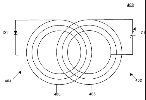
[0028] FIG. 4 is a first circuit for implementing a marker in accordance with
one
embodiment. FIG. 4 illustrates a circuit 400. Circuit 400 may comprise a dual
resonance configuration for marker 200. In one embodiment, circuit 400 may
comprise a first resonant circuit 402 and a second resonant circuit 404.
[0029] In one embodiment, circuit 400 may comprise one or more planarized
coils. The term "planarized coil" as used herein may refer to a coil having a
relatively
flat geometry. For example, the planarized coil may be less than 1 millimeter
(mm)
thick. In another example, the planarized coil may be approximately .2 mm or
200
microns thick. The thickness of any given planarized coil may vary according
to a
given implementation, and the embodiments are not limited in this context.
[0030] In one embodiment, circuit 400 may comprise first resonant circuit 402.
First resonant circuit 402 may comprise an LC combination. For example, first
resonant circuit 402 may comprise a first planarized coil 406 having a pair of
terminals and a capacitor C1 connected to the pair of terminals. Capacitor C1
may
comprise a linear or non-linear capacitor depending on a given implementation.
In
one embodiment, for example, capacitor C1 may comprise a linear capacitor.
First
8
CA 02575174 2007-01-24
WO 2006/049667 PCT/US2005/027995
resonant circuit 402 may be resonant at a first predetermined frequency when
receiving electromagnetic radiation at the first predetermined frequency. The
number
of turns for first planarized coil 406 may vary depending on the frequency of
interrogation signals 104. With an operating frequency of 13.56 MHz, first
planarized
coil 406 may have approximately 10 turns, which may be sufficient for
resonance-and
transmitter coupling needed to induce the appropriate operating voltage. As it
receives the electromagnetic energy from transmitter 102, first resonant
circuit stores
and amplifies the field. The field may be passed to second resonant circuit
404
through the magnetic coupling discussed below.
[0031] In one embodiment, circuit 400 may comprise second resonant circuit
404.
Second resonant circuit 404 may also comprise an LC combination. For example,
second resonant circuit 404 may comprise a second planarized coil 408 having a
pair
of terminals and a non-linear capacitor D1 connected to the pair of terminals.
Non-
linear capacitor D1 may operate as a voltage dependent variable capacitor.
Second
resonant circuit 404 may receive the amplified field from first resonant
circuit 402,
and generates a second resonant signal at a second resonant frequency that is
half the
frequency of the interrogation signal and first resonant signal. In one
embodiment,
for example, second resonant circuit 404 may generate the second resonant
signal at
6.78 MHz with a magnetic field threshold of approximately 10 mA/m rms.
[0032] One advantage of circuit 400 is that it may have a lower magnetic field
threshold as compared to conventional frequency-division circuits. The
frequency-
division process has a minimum threshold below which it will not operate.
Therefore,
the transmitting field at the marker must exceed a minimum magnetic field
threshold.
The lower the threshold, the more sensitive the marker becomes. Conventional
frequency-division markers using an inductor-zener diode combination may have
a
typical turn-on threshold of approximately 100 mA/m rms. In one embodiment,
circuit 400 may output a marker signal at 6.78 MHz with a magnetic field
threshold of
approximately 10 mA/rn rms. As a result, marker 200 using circuit 400 may
result in
a more sensitive marker for improved EAS functionality.
[0033] As shown in FIG. 4, first planarized coil 406 and second planarized
coil
= 408 are positioned so that they overlap each other by a predetermined amount
to form
a double tuned circuit. The amount of overlap determines the degree of mutual
coupling k between the magnetic fields of each resonant circuit. To perform
9
CA 02575174 2007-01-24
WO 2006/049667 PCT/US2005/027995
frequency division, the coupling coefficient k between first planarized coil
406 of first
resonant circuit 402 and second planarized coil 408 of second resonant circuit
404
should be within a range of 0.0 to 0.6. In one embodiment, for example, k may
comprise 0.3 to perform sufficient coupling between the fields.
[0034] Second resonant circuit 404 may utilize a non-linear capacitor for D1.
The
particular non-linear capacitor element may be determined in accordance with a
number of different factors. For example, one factor may be capacitance non-
linearity
(dC/dV). The turn on magnetic field threshold may depend on the dC/dV value at
zero voltage bias condition. The higher the dC/dV value, the lower the
threshold. In
another example, one factor may be capacitive dissipation (Df). The
dissipation
factor determines the amount of energy a resonant LC circuit can store. The
lower the
Df, the more efficient the circuit may operate. Other factors such as inductor-
capacitor ratio and coil loss may also influence the frequency-dividing
functionality.
[0035] In one embodiment, for example, second resonant circuit 404 may use a
MOS device as the non-linear capacitor. A MOS capacitor may offer superior
dC/dV
characteristics relative to conventional capacitors. This may improve device
sensitivity significantly. In addition, proximity deactivation can be achieved
through
the breakdown mechanism of the MOS device. The MOS breakdown voltage can be
controlled by adjusting the thickness of the oxide layers. To deactivate, a
F/2
frequency may be generated and resonated in the inductor-nonlinear capacitor
resonator until the MOS breakdown voltage is reached. An example of a MOS
device
may be described in more detail with reference to FIGS. 5-9.
[0036] FIG. 5A is a sectional view of a capacitance element without a voltage
being applied across the terminals in accordance with one embodiment. FIG. 5A
may
illustrate a variable capacitor 500. Variable capacitor 500 may be implemented
using,
for example, a MOS device. Variable capacitor 500 may comprise a lamination of
a
dielectric insulation material 504 and a semiconductor material 506 disposed
between
a first metal terminal 502 and a second metal terminal 508. First metal
terminal 502
may also be referred to as a gate. The maximum value of the capacitance C may
be
determined by a number of facto'rs, such as the area of first metal terminal
502, the
dielectric constant and thickness of insulation material 504, and so forth.
The
embodiments are not limited in this context.
CA 02575174 2007-01-24
WO 2006/049667 PCT/US2005/027995
[0037] In one embodiment, variable capacitor 500 may include semiconductor
material 506. Semiconductor material 506 may comprise a p-type substrate or an
n-
type substrate, depending upon a given implementatiorn. When semiconductor
material 506 is implemented using a p-type substrate, variable capacitor 500
may
comprise an N-MOS capacitor since the inversion layer contains electrons. When
semiconductor material 506 is implemented using an n-type substrate, variable
capacitor 500 may comprise a P-MOS capacitor.
[0038] In one embodiment, semiconductor material 506 may comprise an
epitaxial layer 506a having a first amount of doping adjacent to insulation
material
504, and a substrate 506b having a second amount of doping between epitaxial
layer
506a and second metal terminal 508. In one embodiment, for example, the first
amount of doping is less than the second amount of doping. Such relative
doping may
decrease the series resistance in semiconductor material 506, as discussed in
more
detail with reference to FIG. 6.
[0039] FIG. 5B is a sectional view of a capacitance element when a voltage is
applied across the terminals in accordance with one embodiment. As shown in
FIG.
513, voltage may be applied across the terminals to deplete the concentration
of charge
carriers in the region of the semiconductor material adjacent to the
insulation material,
thereby decreasing the capacitance of the capacitance element.
[0040] In one embodiment, for example, semiconductor material 506 may be
implemented using an n-type silicon. When a negative voltage is applied to
first
metal terminal 502 relative to second metal terminal 508, charge carriers in
the lightly
doped epitaxial layer 506a are repelled from the interface of insulation
material 504
and the lightly doped epitaxial layer 506a in a region adjacent to insulation
material
504. The depletion of charge carriers may expose silicon ions in the region
adjacent
to insulation material 504. This may establish a second capacitance in series
with a
first capacitance established by insulation material 504. The second
capacitance
combined with the first capacitance may decrease the overall capacitance of
variable
capacitor 500. As the voltage becomes more negative, the overall capacitance
of
variable capacitor 500 is decreased.
[0041] In one embodiment, for example, semiconductor material 506 may be
implemented using a p-type silicon. When a positive voltage is applied to
first metal
terminal 502 relative to second metal terminal 508, charge carriers in the
lightly
11
CA 02575174 2007-01-24
WO 2006/049667 PCT/US2005/027995
doped epitaxial layer 506a are repelled from the interface of insulation
material 504
and the lightly doped epitaxial layer 506a in a region adjacent to insulation
material
504. The depletion of charge carriers may expose silicon ions in the region
adjacent
to insulation material 504. This may establish a second capacitance in series
with-a
first capacitance established by insulation material 504. The second
capacitance
combined with the first capacitance may decrease the overall capacitance of
variable
capacitor 500. As the voltage becomes more negative, the overall capacitance
of
variable capacitor 500 is decreased.
[0042] FIG. 5C is a sectional view of a capacitance element when a voltage is
applied across the terminals in accordance with one embodiment. As shown in
FIG.
5C, voltage may be applied across the terminals to enhance the concentration
of
charge carriers in the region of the semiconductor material adjacent to
insulation
material 504, thereby increasing the capacitance of the capacitance element.
[0043] Referring again to the example where semiconductor material 506 is
implemented using an n-type silicon, when a positive voltage is applied to
first metal
terminal 502 relative to second terminal 508, charge carriers in the lightly
doped
epitaxial layer 506a are attracted to the interface of insulation material 504
and the
lightly doped epitaxial layer 506a to enhance the concentration of charge
carriers in
the lightly doped epitaxial layer 506a in the region adjacent to insulation
material 504.
The enhancement of charge carriers may reduce the region of exposed ions and
thereby increase the overall capacitance of variable capacitor 500. As the
voltage
applied to first metal terminal 502 becomes more positive, the overall
capacitance of
variable capacitor 500 is increased.
[0044] Referring again to the example where semiconductor material 506 is
implemented using a p-type silicon, when a negative voltage is applied to
first metal
terminal 502 relative to second terminal 508, charge carriers in the lightly
doped
epitaxial layer 506a are attracted to the interface of insulation material 504
and the
lightly doped epitaxial layer 506a to enhance the concentration of charge
carriers in
the lightly doped epitaxial layer 506a in the region adjacent to insulation
material 504.
The enhancement of charge carriers may reduce the region of exposed ions and
thereby increase the overall capacitance of variable capacitor 500. As the
voltage
applied to first metal terminal 502 becomes more positive, the overall
capacitance of
variable capacitor 500 is increased.
12
CA 02575174 2007-01-24
WO 2006/049667 PCT/US2005/027995
[0045] FIG. 6 illustrates a graph of capacitance versus gate voltage in
accordance
with one embodiment. FIG. 6 illustrates a typical CV curve for a p-substrate
MOS
capacitor. Three major operational regions are also indicated. A circuit
insert shows
the overall capacitance during the depletion mode.
[0046] In one embodiment, FIG. 6 illustrates the relation of capacitance and
applied gate voltage of a P-substrate material. There are three main operation
regions
for variable capacitor 500, that is, accumulation, depletion, and inversion.
With a
negative gate voltage, the device is in the accumulation mode. The negative
gate
voltage attracts the majority carrier (in this case, hole carrier), which
forms a
capacitor mainly contributed by the oxide layer (C;). The unit capacitance
(CMos)'
may be expressed as part of equation (1) as follows:
CMOs = Ci = E (1)
where si and d are the permittivity and the thickness of the insulator layer.
[0047] As the gate voltage becomes more positive, the MOS device enters into
the
depletion mode, where the majority hole carriers are expelled away from the
Si,
insulator junction. This forms an addition capacitor (depletion capacitance
Cd) in
series connection with Ci. Therefore we have:
_ Ci.Cd
CMOS (2)
C' + C d
C ~' d= W' (3)
d
where ss;, and Wd are the permittivity of Silicon, and width of the depletion
layer
respectively. The net MOS capacitance drops almost linearly with the increase
of the
gate voltage (in the case of p-substrate MOS device), until the voltage
reaches the
inversion threshold. At this moment, the silicon-insulator interface is
flooded with the
electron carriers, and the width of the depletion region reaches its maximum.
As a
result, the overall capacitance CMos remains constant, as long as the signal
frequency
is high, and the carrier cannot respond due to limited drift speed. With a low
13
CA 02575174 2007-01-24
WO 2006/049667 PCT/US2005/027995
frequency condition, the capacitance C,nos reverts back to the value of Ci, as
shown in
FIG. 6.
[0048] FIG. 7 illustrates a graph of the measured capacitance and dissipation
data
(CV/DV) characteristics of a MOS device in accordance with one embodiment.
FIG.
7 shows the CV/DV for a p-type substrate MOS capacitor with a measuring
frequency
set at 1 Megahertz (MHz). The CV curve substantially conforms to the theoretic
trend depicted in FIG. 7. There is approximately eight (8) times of
capacitance swing
as the gate voltage, such as from 80 pF to 630 pF, for example. It is also
worthy to
note that the maximum rate of capacitance change occurs at approximately
negative
1.3 volts. In an EAS application, it may be critical to design the device
material and
process condition so that such a maximum rate change occurs around zero volt
region.
This can be achieved through careful selection of gate metal material. The
work
function of the metal will be effective in modifying the flat band voltage,
thus shifting
the CV curve along the voltage axis. Some of the suitable gate materials may
include,
for example, Au, Mo, Ta, and polysilicon. The embodiments are not limited in
this
context.
[0049] FIG. 7 may also illustrate the dissipation characteristics of variable
capacitor 500. The dissipation factor (D) is defined as the ratio of energy
loss vs.
energy storage in the capacitor, as shown below for a series circuits model:
D=w=C=R (4)
where cw is the operating angular frequency, and R is the series resistance,
which may
result from contact or the bulk silicon layer.
[0050] The trend of the dissipation may be similar to the CV curve. This may
indicate significant series bulk resistance, resulting in substantial loss
especially at a
high capacitance region. To reduce such a bulk resistance, it may be desirable
to use
a high doping concentration for the substrate. This may also negatively impact
the
device performance, however, by reducing the characteristics of capacitance
modulation.
[0051] FIG. 8 illustrates a graph of carrier concentration versus capacitance
ratio
in accordance with one embodiment. FIG. 8 shows the maximum capacitance ratio
as
a function of carrier concentration for a MOS capacitor with 100-Angstrom gate
14
CA 02575174 2007-01-24
WO 2006/049667 PCT/US2005/027995
dielectrics. The use of highly doped silicon substrate is shown to reduce the
maximum capacitance ratio. It is possible to resolve this conflict by using a
highly
doped silicon wafer with a thin epitaxial layer with a low carrier
concentration, since
the maximum depletion width is normally less than one micron. An example of a
thickness for an epitaxial layer may comprise 1 m. The embodiments, however,
are
not limited in this context.
[0052] The MOS structure may be developed in a number of different ways. For
example, the MOS structure may start with an insulated substrate. A bottom
conductor layer pattern may be deposited. The bottom layer may be followed by
depositing a thin silicon layer with a predetermined level of impurity
concentration.
A thin oxide layer may then be created by either deposition or thermal growth
over
the silicon layer, followed by another metallization process to form the top
electrode.
Finally a patterning operation may be performed to expose the bottom electrode
for
contact purpose.
[0053] In one embodiment, variable capacitor 500 may be developed using
printed electronics techniques. Printed electronics techniques may offer the
potential
of lower costs, a larger printing area, flexible substrates, and so forth. In
one
embodiment, for example, the complexity of the above development operations
can
be reduced by printing each respective layer, and obviating the patterning
operations.
The printing operation may start with a printable/treatable substrate. In one
embodiment, the substrate may be a flexible substrate. The bottom electrode
may be
-printed. The semiconductor layer may be printed or deposited. The thin
dielectric
layer may be printed or deposited. Finally, the top electrode may be printed.
[0054] FIG. 9 is a second circuit for implementing a marker in accordance with
one embodiment. FIG. 9 illustrates a circuit 900. Circuit 900 may comprise a
different dual resonance configuration for marker 200. In one embodiment,
circuit
900 may comprise a first resonant circuit 902 and a second resonant circuit
904. First
resonant circuit 902 and second resonant circuit 904 may be similar to first
resonant
circuit 402 and second resonant circuit 404, respectively. First resonant
circuit 902
may comprise a first planarized coil 906 and a linear capacitor Cl. Second
resonant
circuit 904 may comprise a second planarized coil 908 and a non-linear
capacitor D1.
[0055] In one embodiment, circuit 900 comprises a coil arrangement to achieve
a
coupling of 0.3. Circuit 900 may illustrate a dual-resonance configuration
having one
CA 02575174 2007-01-24
WO 2006/049667 PCT/US2005/027995
LC resonant circuit within another LC resonant circuit. As shown in circuit
900,
second resonant circuit 904 may be nested within first planarized coil 906 of
first
resonant circuit 902. By placing the F resonant circuit outside the F/2
resonant
circuit, this configuration may provide improved sensitivity by increasing the
field
capture area. Although circuit 900 shows second resonant circuit 904 being
nested
within first planarized coil 906, it may be appreciated that the reverse
configuration
may be implemented and still fall within the scope of the embodiments. The
embodiments are not limited in this context.
[0056] Frequency division markers such as circuits 400 and 900 may be
manufactured in a number of different ways. For example, the inductor metal
pattern
can be deposited, etched, stamped, or otherwise placed on a thin and flexible
substrate. The non-linear capacitor may be bonded to the inductor terminals.
Conventional bonding techniques may result in a marker having a slight bump
due to
the placement of the nonlinear capacitor element. To avoid this bump, a
printed
semiconductor process may be used. The printed semiconductor process can
fabricate
conductor patterns and the nonlinear capacitor element in a single, flexible
substrate
in a mass-production scale. The embodiments are not limited in this context.
[0057] Although the embodiments have been discussed in terms of dual-
resonance configurations, it may be appreciated that a single LC resonant
circuit may
also be implemented using the principles discussed herein. For example, a
single LC
resonant circuit comprising a non-linear capacitor (e.g., variable capacitor
500) and
planarized coil may be configured to operate in the 13.56 MHz band. The higher
operating frequencies may result in reduced geometries and smaller form
factors for
the single LC resonant circuit, while still emitting a detectable resonant
signal at the
appropriate frequency. The embodiments are not limited in this context.
[0058] Some embodiments may be implemented using an architecture that may
vary in accordance with any number of factors, such as desired computational
rate,
power levels, heat tolerances, processing cycle budget, input data rates,
output data
rates, memory resources, data bus speeds and other performance constraints.
For
example, an embodiment may be implemented using software executed by a general-
purpose or special-purpose processor. In another example, an embodiment may be
implemented as dedicated hardware, such as a circuit, an application specific
integrated circuit (ASIC), Programmable Logic Device (PLD) or digital signal
16
CA 02575174 2007-01-24
WO 2006/049667 PCT/US2005/027995
processor (DSP), and so forth. In yet another example, an embodiment may be
implemented by any combination of programmed general-purpose computer
components and custom hardware components. The embodiments are not limited in
this context.
[0059] Some embodiments may be described using the expression "coupled" and
"connected" along with their derivatives. It should be understood that these
terms are
not intended as synonyms for each other. For example, some embodiments may be
described using the term "connected" to indicate that two or more elements are
in
direct physical or electrical contact with each other. In another example,
some
embodiments may be described using the term "coupled" to indicate that two or
more
elements are in direct physical or electrical contact. The term "coupled,"
however,
may also mean that two or more elements are not in direct contact with each
other, but
yet still co-operate or interact with each other. The embodiments are not
limited in
this context.
[0060] While certain features of the embodiments have been illustrated as
described herein, many modifications, substitutions, changes and equivalents
will now
occur to those skilled in the art. It is therefore to be understood that the
appended
claims are intended to cover all such modifications and changes as fall within
the true
spirit of the embodiments.
17