Note: Descriptions are shown in the official language in which they were submitted.
CA 02575314 2007-01-25
WO 2006/014929 PCT/US2005/026448
SYSTEM AND METHOD FOR MICRO-ELECTROMECHANICAL OPERATING OF AN INTERFEROMETRIC
MO
DULATOR
CROSS-REFERENCE TO RELATED APPLICATIONS
[0001] This application is a continuation-in-part of the following: U.S.
Application
Serial No. 10/909,228, filed July 29, 2004; and U.S. Application Serial No.
11/048,662, filed
January 27, 2005; both of which are hereby incorporated by reference in their
entireties. This
application also claims priority to the following: U.S. Provisional
Application No. 60/613,466,
filed September 27, 2004; U.S. Provisional Application No. 60/613,499, filed
September 27, 2004;
and U.S. Provisional Application No. 60/658,867, filed March 4, 2005; all of
which are hereby
incorporated herein by reference in their entireties.
BACKGROUND
Field of the Invention
[0002] This invention relates to microelectromechanical systems for use as
interferometric modulators. More particularly, this invention relates to
systems and methods for
improving the micro-electromechanical operation of interferometric modulators.
Description of the Related Art
[0003] Microelectromechanical systems (MEMS) include micro mechanical
elements,
actuators, and electronics. Micromechanical elements may be created using
deposition, etching,
and or other micromachining processes that etch away parts of substrates
and/or deposited material
layers or that add layers to form electrical and electromechanical devices.
One type of MEMS
device is called an interferometric modulator. As used herein, the term
interferometric modulator
or interferometric light modulator refers to a device that selectively absorbs
and/or reflects light
using the principles of optical interference. In certain embodiments, an
interferometric modulator
may comprise a pair of conductive plates, one or both of which may be
transparent and/or reflective
in whole or part and capable of relative motion upon application of an
appropriate electrical
signal. In a particular embodiment, one plate may comprise a stationary layer
deposited on a
substrate and the other plate may comprise a metallic membrane separated from
the stationary layer
by an air gap. As described herein in more detail, the position of one plate
in relation to
another can change the optical interference of light incident on the
interferometric modulator. Such
devices have a wide range of applications, and it would be beneficial in the
art to utilize and/or
modify the characteristics of these types of devices so that their features
can be exploited in
improving existing products and creating new products that have not yet been
developed.
-1-
CA 02575314 2007-01-25
WO 2006/014929 PCT/US2005/026448
Summary
[0004] The system, method, and devices of the invention each have several
aspects, no
single one of which is solely responsible for its desirable attributes.
Without limiting the scope of
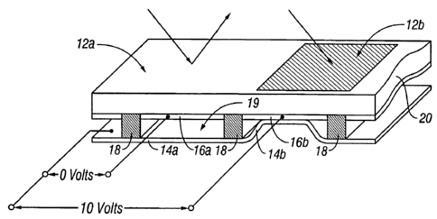
this invention, its more prominent features will now be discussed briefly.
After considering this
discussion, and particularly after reading the section entitled "Detailed
Description of Certain
Embodiments" one will understand how the features of this invention provide
advantages over
other display devices.
[0005] One aspect of the invention provides an interferometric modulator,
which
includes a first layer, a second layer and a member. The first layer includes
a first reflective planar
portion. The second layer includes a second reflective planar portion located
substantially parallel
to the first reflective planar portion. The second layer is movable between a
first position and a
second position. The first position is located at a first distance from the
first layer. The second
position is located at a second distance from the first layer. The second
distance is greater than the
first distance. The member includes a surface that is located between the
first layer and second
layer. The member defines one or more gap regions between the first layer and
the second layer
when the second layer is in the first position, wherein the second layer in
the one or more gap
regions does not contact either the first layer or the member.
[0006] Another aspect of the invention provides a microelectromechanical
device,
which includes a first surface, a second surface and a third surface. The
second surface is located
substantially parallel to the first surface. The second surface is movable
between a first position
and a second position. The first position is located at a first distance from
the first surface. The
second position is located at a second distance from the first surface. The
second distance is greater
than the first distance. The third surface is located between the first
surface and the second surface.
The third surface defines one or more gap regions between the first surface
and the second surface
when the second surface is in the first position, wherein the second surface
in the one or more gap
regions does not contact either the first surface or the third surface.
[0007] Another aspect of the invention provides a microelectromechanical
device,
which includes a first layer; a second layer and a plurality of members. The
second layer is located
substantially parallel to the first layer. The second layer is movable between
a first position and a
second position. The first position is a first distance from the first layer.
The second position is a
second distance from the first layer. The second distance is greater than the
first distance. Each of
the plurality of members includes a surface located between the first layer
and second layer. The
plurality of members define one or more gap regions between the first layer
and the second layer
when the second layer is in the first position, wherein the second layer in
the one or more gap
regions does not contact either the first layer or the plurality of members.
[0008] Still another aspect of the invention provides a microelectromechanical
device,
which includes a first surface, a second surface and at least one structure on
at least one of the first
-2-
CA 02575314 2007-01-25
WO 2006/014929 PCT/US2005/026448
surface and the second surface. The second surface is located substantially
parallel to the first
surface. The second surface is movable relative to the first surface between a
driven position and
an undriven position. The driven position is closer to the first surface than
is the undriven position.
The at least one structure is compressed by the first surface and the second
surface when the second
surface is in the driven position. The at least one structure provides a force
to the second surface
when the second surface is in the driven position. The force assists movement
of the second surface
from the driven position toward the undriven position.
[0009] Still another aspect of the invention provides a method of making an
interferometric modulator. The method includes: providing a first layer,
forming a second layer and
forming a member comprising a surface. The first layer includes a first
reflective planar portion.
The second layer includes a second reflective planar portion. The second
reflective planar portion
is located substantially parallel to the first reflective planar portion. The
second layer is movable
between a first position and a second position. The first position is at a
first distance from the first
layer. The second position is at a second distance from the first layer. The
second distance is
greater than the first distance. The surface of the member is located between
the first layer and the
second layer. The member defines one or more gap regions between the first
layer and the second
layer when the second layer is in the first position, wherein the second layer
in the one or more gap
regions does not contact either the first layer or the member.
[0010] A further aspect of the invention provides a microelectromechanical
device
produced by a method. The method includes: providing a first layer, providing
a second layer and
providing a member comprising a surface. The first layer includes a first
reflective planar portion.
The second layer includes a second reflective planar portion. One of the first
reflective planar
portion and the second reflective planar portion may be partially reflective.
The second reflective
planar portion is located substantially parallel to the first reflective
planar portion. The second layer
is movable between a first position and a second position. The first position
is at a first distance
from the first layer. The second position is at a second distance from the
first layer. The second
distance is greater than the first distance. The surface of the member is
located between the first
layer and the second layer. The member defines one or more gap regions between
the first layer
and the second layer when the second layer is in the first position, wherein
the second layer in the
one or more gap regions does not contact either the first layer or the member.
[0011] A further aspect of the invention provides a method of operating a
microelectromechanical device. Here, the device includes a first layer, a
second layer and a
member. The second layer of the device is located substantially parallel to
the first layer. The
member includes a surface intervening between the first layer and second
layer. The surface of the
member is located between only portions of the first layer and the second
layer. The method of
operating the device includes moving the second layer relative to the first
layer from an undriven
position to a driven position. The driven position is closer to the first
layer than is the undriven
-3-
CA 02575314 2007-01-25
WO 2006/014929 PCT/US2005/026448
position. The method further includes contacting the member with at least one
of the first layer and
the second layer so as to stop the movement of the second layer at the driven
position, the member
defining one or more gap regions between the first layer and the second layer
when the second layer
is in the driven position, wherein the second layer in the one or more gap
regions does not contact
either the first layer or the member..
100121 A further aspect of the invention provides a microelectromechanical
device.
The device includes first means for partially reflecting and partially
transmitting incident light and
second means for substantially reflecting incident light. The device further
includes means for
moving the first means relative to the second means between a driven position
and an undriven
position. The device further includes means for providing a separation between
the first means and
the second means when the second means is in the driven position. The driven
position is closer to
the first means than is the undriven position. The first means may include,
for example, a partial
mirror surface. The second means may include, for example, a full mirror
surface. The means for
moving may include, for example, a deformable layer. The means for providing
separation may
include, for example, at least one of a bump, a landing pad or a spring clip
[0013] A further aspect of the invention provides a microelectromechanical
device.
The device includes: first means for partially reflecting and partially
transmitting incident light and
second means for substantially reflecting incident light. The device further
includes means for
moving the first means relative to the second means between a driven position
and an undriven
position, and means for applying a force on the second means in a direction
toward the undriven
position when the second means is in the driven position. The first means may
include, for
example, a partial mirror surface. The second means may include, for example,
a full mirror
surface. The means for moving may include, for example, a deformable layer.
The means for
applying force may include, for example, a spring clip, or, as another
example, a bump or a landing
pad that includes an elastomeric material.
[0014] A still further aspect of the invention provides an interferometric
modulator.
The interferometric modulator includes a first layer, a second layer and at
least one bump on the at
least one of the first layer and the second layer. The first layer includes a
first reflective planar
portion. The second layer includes a second reflective planar portion that is
located substantially
parallel to the first reflective planar portion. The second layer is movable
between a driven position
and an undriven position. The driven position is closer to the first layer
than the undriven position.
The at least one bump is configured to prevent the first layer and the second
layer from contacting
each other.
[0015] A still further aspect of the invention provides an interferometric
modulator,
which includes a first layer, a second layer and at least one landing pad
located between the first
layer and the second layer. The first layer includes a first reflective planar
portion. The second
layer includes a second reflective planar portion that is located
substantially parallel to the first
-4-
CA 02575314 2007-01-25
WO 2006/014929 PCT/US2005/026448
reflective planar portion. The second layer is movable between a driven
position and an undriven
position. The driven position is closer to the first layer than the undriven
position. The at least one
landing pad includes a contact area where one of the first layer and the
second layer contacts while
not contacting the other when the second layer is in the driven position.
[0016] A still further aspect of the invention provides an interferometric
modulator.
The interferometric modulator includes a first layer, a second layer and at
least one spring member
placed between the at least one of the first layer and the second layer. The
first layer includes a first
reflective planar portion. The second layer includes a second reflective
planar portion that is
located substantially parallel to the first reflective planar portion. One of
the first reflective planar
portion and the second reflective planar portion may be partially reflective.
The second layer is
movable between a driven position and an undriven position. The driven
position is closer to the
first layer than the undriven position. The at least one spring member is
compressible by at least
one of the first layer and second layer as the second layer moves toward the
driven position. The at
least one spring member is configured to apply force to the second layer in a
direction toward the
undriven position when the second layer is in the driven position.
[0017] Another embodiment provides a display system comprising an
interferometric
modulator, a display, a processor and a memory device. The processor is in
electrical
communication with the display and configured to process image data. The
memory device is in
electrical communication with the processor.
[0018] Another embodiment provides a method of making a MEMS device, such as a
MEMS device that includes an interferometric modulator. The method includes
forming a first
electrode, depositing a dielectric material over at least a portion of the
first electrode, then removing
a portion of the dielectric material from over the first electrode, thereby
forming a variable
thickness dielectric layer. The method further includes forming a second
electrode over at least a
portion of the variable thickness dielectric layer. In an embodiment, a
sacrificial layer is deposited
over at least a portion of the dielectric material that is over the first
electrode. The sacrificial layer
and at least a portion of the dielectric material may be removed during a
later etching step. Another
embodiment provides an interferometric modulator made by such a method.
[0019] Another embodiment provides a method of making an interferometric
modulator. The method includes forming a first electrode and depositing a
dielectric layer over at
least a portion of the first electrode. The method further includes removing a
portion of the
dielectric layer to form a variable thickness dielectric layer, depositing a
sacrificial layer over the
variable thickness dielectric layer, planarizing the sacrificial layer, and
forming a second electrode
over the sacrificial layer. Another embodiment provides an interferometric
modulator made by
such a method.
[0020] Another embodiment provides a method of making an interferometric
modulator. The method includes forming a first electrode and depositing a
dielectric layer over at
-5-
CA 02575314 2007-01-25
WO 2006/014929 PCT/US2005/026448
least a portion of the first electrode. The method further includes removing a
portion of the
dielectric layer to form a variable thickness dielectric layer, depositing a
sacrificial layer over the
variable thickness dielectric layer, depositing a planarization layer over the
sacrificial layer, and
forming a second electrode over the planarization layer. Another embodiment
provides an
interferometric modulator made by such a method.
Brief Description of the Drawinjzs
[0021] FIG. 1 is an isometric view depicting a portion of one embodiment of an
interferometric modulator display in which a movable reflective layer of a
first interferometric
modulator is in a relaxed position and a movable reflective layer of a second
interferometric
modulator is in an actuated position.
[0022] FIG. 2 is a system block diagram illustrating one embodiment of an
electronic
device incorporating a 3x3 interferometric modulator display.
[0023] FIG. 3 is a diagram of movable mirror position versus applied voltage
for one
exemplary embodiment of an interferometric modulator of FIG. 1.
[0024] FIG. 4 is an illustration of a set of row and column voltages that may
be used to
drive an interferometric modulator display.
100251 FIGS. 5A and 5B illustrate one exemplary timing diagram for row and
column
signals that may be used to write a frame of display data to the 3x3
interferometric modulator
display of FIG. 2.
[0026] FIGS. 6A and 6B are system block diagrams illustrating an embodiment of
a
visual display device comprising a plurality of interferometric modulators.
[0027] FIG. 7A is a cross section of the device of FIG. 1.
[0028] FIG. 7B is a cross section of an alternative embodiment of an
interferometric
modulator.
[0029] FIG. 7C is a cross section of another alternative embodiment of an
interferometric modulator.
[0030] FIG 7D is a cross section of yet another alternative embodiment of an
interferometric modulator.
[0031] FIG. 7E is a cross section of an additional alternative embodiment of
an
interferometric modulator.
[0032] Figure 8 is a perspective view of an interferometric modulator array
which uses
micro-electromechanical system technology.
[0033] Figure 9A is a schematic cross-sectional view of the interferometric
modulator
array of Figure 7 taken along line 8A-8A of Figure 7.
[0034] Figure 9B is a schematic cross-sectional view of another embodiment of
the
interferometric modulator array utilizing micro-electromechanical system
technology.
-6-
CA 02575314 2007-01-25
WO 2006/014929 PCT/US2005/026448
[0035] Figure 10A is a side cross-sectional view of an embodiment of the
interferometric modulator including landing pads with the modulator shown in
the undriven state.
[0036] Figure lOB is a side cross-sectional view of the embodiment of Figure
9A in
the driven state.
[0037] Figures lOC-l0I are side cross-sectional views of embodiments of the
interferometric modulator, illustrating various configurations of landing
pads.
[0038] Figure IOJ is a top cross-sectional view of an embodiment of the
interferometric modulator taken along line 9J-9J of Figure 9A and illustrating
various shapes of
landing pads.
[0039] Figure 11 is a flowchart illustrating a method of manufacturing a MEMS
device having a variable thickness dielectric layer.
[0040] Figure 12 is a cross-sectional view schematically illustrating an
alternative
embodiment of a MEMS device having a variable thickness dielectric layer.
[0041] Figure 13 is a cross-sectional view schematically illustrating the
formation of a
lower electrode 502 in accordance with an embodiment.
[0042] Figure 14 is a cross-sectional view schematically illustrating the
formation of a
dielectric layer 540 (including a lower portion 550 and an upper portion 560)
on the stationary layer
502 and over the substrate 500 of Figure 13.
[0043] Figures 15 and 16 are cross-sectional views schematically illustrating
the
formation of a variable thickness dielectric layer 570 (including "stops" 565)
on the stationary layer
502 of Figure 13 by removing parts of the upper portion 560 of dielectric
layer 540 of Figure 14.
[0044] Figure 17 is cross-sectional views schematically illustrating the
formation of a
sacrificial layer 710, support structures 720, and an upper electrode 730 of
an interferometric
modulator.
[0045] Figure 18 is a cross-sectional view schematically illustrating the
removal of the
sacrificial layer 710 and the removal of parts of the lower portion 550 of the
dielectric layer 570 of
Figure 17.
[0046] Figure 19 shows cross-sectional views schematically illustrating an
interferometric modulator 1800 comprising a stationary layer 502, a deformable
layer 506, and a
variable thickness dielectric layer 920 that substantially prevents contact
between the first electrode
502 and the second electrode 506.
[0047] Figure 20 shows cross-sectional views schematically illustrating the
formation
of a sacrificial layer 710, support structures 720, and an upper electrode 731
of an interferometric
modulator.
[0048] Figure 21 is a cross-sectional view schematically illustrating an
interferometric
modulator.
-7-
CA 02575314 2007-01-25
WO 2006/014929 PCT/US2005/026448
[0049] Figure 22A is a side cross-sectional view of an embodiment of the
interferometric modulator with bumps showing the modulator in the undriven
state.
[0050] Figure 22B is a side cross-sectional view of the embodiment of Figure
22A in
the driven state.
100511 Figures 22C-22E are side cross-sectional views of embodiments of the
interferometric modulator illustrating various configurations of bumps.
[0052] Figure 23A is a side cross-sectional view of an embodiment of the
interferometric modulator with spring clips showing the modulator in the
undriven state.
[0053] Figure 23B is a side cross-sectional view of the embodiment of Figure
23A in
the driven state.
[0054] Figures 23C-23F are side cross-sectional views of embodiments of the
interferometric modulator illustrating various configurations of spring clips.
[0055] Figure 24A is a side cross-sectional view of one embodiment of a three
state
interferometric modulator in the undriven state.
100561 Figure 24B is a side cross-sectional view of the three state
interferometric
modulator of Figure 24A in the driven state.
[0057] Figure 24C is a side cross-sectional view of the three state
interferometric
modulator of Figure 24A in the reverse driven state.
[0058] Figure 24D is a side cross-sectional view of another embodiment of the
interferometric modulator in the undriven state.
[0059] Figure 24E is a side cross-sectional view of another embodiment of the
interferometric modulator in the undriven state.
[0060] Figure 25A is a side cross-sectional view of an alternative embodiment
of an
interferometric modulator shown in the undriven state.
[0061] Figure 25B is a top plan view of the interferometric modulator of
Figure 25A,
shown in the undriven state.
[0062] Figure 25C is a side view of the interferometric modulator of Figure
25A,
shown in the driven state.
[0063] Figure 25D is a top plain view of the interferometric modulator of
Figure 20C,
shown in the driven state.
Detailed Description of Preferred Embodiments
[0064] The following detailed description is directed to certain specific
embodiments
of the invention. However, the invention can be embodied in a multitude of
different ways. In this
description, reference is made to the drawings wherein like parts are
designated with like numerals
throughout. As will be apparent from the following description, the
embodiments may be
implemented in any device that is configured to display an image, whether in
motion (e.g., video) or
-8-
CA 02575314 2007-01-25
WO 2006/014929 PCT/US2005/026448
stationary (e.g., still image), and whether textual or pictorial. More
particularly, it is contemplated
that the embodiments may be implemented in or associated with a variety of
electronic devices such
as, but not limited to, mobile telephones, wireless devices, personal data
assistants (PDAs), hand-
held or portable computers, GPS receivers/navigators, cameras, MP3 players,
camcorders, game
consoles, wrist watches, clocks, calculators, television monitors, flat panel
displays, computer
monitors, auto displays (e.g., odometer display, etc.), cockpit controls
and/or displays, display of
camera views (e.g., display of a rear view camera in a vehicle), electronic
photographs, electronic
billboards or signs, projectors, architectural structures, packaging, and
aesthetic structures (e.g.,
display of images on a piece of jewelry). MEMS devices of similar structure to
those described
herein can also be used in non-display applications such as in electronic
switching devices.
[0065] Driving an interferometric modulator may result in contact between a
deformable layer and a stationary layer. Such contact may be undesirable and
may result in damage
to the device, potentially resulting in performance degradation. Various
embodiments provides
structures (such as landing pads, bumps and spring clips) and methods for
reducing such damage.
[0066] One interferometric modulator display embodiment comprising an
interferometric MEMS display element is illustrated in Figure 1. In these
devices, the pixels are in
either a bright or dark state. In the bright ("on" or "open") state, the
display element reflects a large
portion of incident visible light to a user. When in the dark ("off' or
"closed") state, the display
element reflects little incident visible light to the user. Depending on the
embodiment, the light
reflectance properties of the "on" and "off' states may be reversed. MEMS
pixels can be
configured to reflect predominantly at selected colors, allowing for a color
display in addition to
black and white.
[0067] Figure 1 is an isometric view depicting two adjacent pixels in a series
of pixels
of a visual display, wherein each pixel comprises a MEMS interferometric
modulator. In some
embodiments, an interferometric modulator display comprises a row/column array
of these
interferometric modulators. Each interferometric modulator includes a pair of
reflective layers
positioned at a variable and controllable distance from each other to form a
resonant optical cavity
with at least one variable dimension. In one embodiment, one of the reflective
layers may be
moved between two positions. hi the first position, referred to herein as the
relaxed position, the
movable reflective layer is positioned at a relatively large distance from a
fixed partially reflective
layer. In the second position, referred to herein as the actuated position,
the movable reflective
layer is positioned more closely adjacent to the partially reflective layer.
Incident light that reflects
from the two layers interferes constructively or destructively depending on
the position of the
movable reflective layer, producing either an overall reflective or non-
reflective state for each pixel.
[0068] The depicted portion of the pixel array in Figure 1 includes two
adjacent
interferometric modulators 12a and 12b. In the interferometric modulator 12a
on the left, a
movable reflective layer 14a is illustrated in a relaxed position at a
predetermined distance from an
-9-
CA 02575314 2007-01-25
WO 2006/014929 PCT/US2005/026448
optical stack 16a, which includes a partially reflective layer. In the
interferometric modulator 12b
on the right, the movable reflective layer 14b is illustrated in an actuated
position adjacent to the
optical stack 16b.
[0069] The optical stacks 16a and 16b (collectively referred to as optical
stack 16), as
referenced herein, typically comprise of several fused layers, which can
include an electrode layer,
such as indium tin oxide (ITO), a partially reflective layer, such as
chromium, and a transparent
dielectric. The optical stack 16 is thus electrically conductive, partially
transparent and partially
reflective, and may be fabricated, for example, by depositing one or more of
the above layers onto a
transparent substrate 20. In some embodiments, the layers are patterned into
parallel strips, and
may form row electrodes in a display device as described further below. The
movable reflective
layers 14a, 14b may be formed as a series of parallel strips of a deposited
metal layer or layers
(orthogonal to the row electrodes of 16a, 16b) deposited on top of posts 18
and an intervening
sacrificial material deposited between the posts 18. When the sacrificial
material is etched away,
the movable reflective layers 14a, 14b are separated from the optical stacks
16a, 16b by a defined
gap 19. A highly conductive and reflective material such as aluminum may be
used for the
reflective layers 14, and these strips may form column electrodes in a display
device.
[0070] With no applied voltage, the cavity 19 remains between the movable
reflective
layer 14a and optical stack 16a, with the movable reflective layer 14a in a
mechanically relaxed
state, as illustrated by the pixel 12a in Figure 1. However, when a potential
difference is applied to
a selected row and column, the capacitor formed at the intersection of the row
and column
electrodes at the corresponding pixel becomes charged, and electrostatic
forces pull the electrodes
together. If the voltage is high enough, the movable reflective layer 14 is
deformed and is forced
against the optical stack 16. A dielectric layer (not illustrated in this
Figure) within the optical stack
16 may prevent shorting and control the separation distance between layers 14
and 16, as illustrated
by pixel 12b on the right in Figure 1. The behavior is the same regardless of
the polarity of the
applied potential difference. In this way, row/column actuation that can
control the reflective vs.
non-reflective pixel states is analogous in many ways to that used in
conventional LCD and other
display technologies.
[0071] Figures 2 through 5 illustrate one exemplary process and system for
using an
array of interferometric modulators in a display application.
[0072] Figure 2 is a system block diagram illustrating one embodiment of an
electronic device that may incorporate aspects of the invention. In the
exemplary embodiment, the
electronic device includes a processor 21 which may be any general purpose
single- or multi-chip
microprocessor such as an ARM, Pentiurri , Pentium Ie, Pentium III , Pentium
IV , Pentium Pro,
an 8051, a MIPS , a Power PC , an ALPHA , or any special purpose
microprocessor such as a
digital signal processor, microcontroller, or a programmable gate array. As is
conventional in the
art, the processor 21 may be configured to execute one or more software
modules. In addition to
-10-
CA 02575314 2007-01-25
WO 2006/014929 PCT/US2005/026448
executing an operating system, the processor may be configured to execute one
or more software
applications, including a web browser, a telephone application, an email
program, or any other
software application.
[0073] In one embodiment, the processor 21 is also configured to communicate
with
an array driver 22. In one embodiment, the array driver 22 includes a row
driver circuit 24 and a
column driver circuit 26 that provide signals to a display array or pane130.
The cross section of the
array illustrated in Figure 1 is shown by the lines 1-1 in Figure 2. For MEMS
interferometric
modulators, the row/column actuation protocol may take advantage of a
hysteresis property of these
devices illustrated in Figure 3. It may require, for example, a 10 volt
potential difference to cause a
movable layer to deform from the relaxed state to the actuated state. However,
when the voltage is
reduced from that value, the movable layer maintains its state as the voltage
drops back below 10
volts. In the exemplary embodiment of Figure 3, the movable layer does not
relax completely until
the voltage drops below 2 volts. There is thus a range of voltage, about 3 to
7 V in the example
illustrated in Figure 3, where there exists a window of applied voltage within
which the device is
stable in either the relaxed or actuated state. This is referred to herein as
the "hysteresis window"
or "stability window." For a display array having the hysteresis
characteristics of Figure 3, the
row/column actuation protocol can be designed such that during row strobing,
pixels in the strobed
row that are to be actuated are exposed to a voltage difference of about 10
volts, and pixels that are
to be relaxed are exposed to a voltage difference of close to zero volts.
After the strobe, the pixels
are exposed to a steady state voltage difference of about 5 volts such that
they remain in whatever
state the row strobe put them in. After being written, each pixel sees a
potential difference within
the "stability window" of 3-7 volts in this example. This feature makes the
pixel design illustrated
in Figure 1 stable under the same applied voltage conditions in either an
actuated or relaxed pre-
existing state. Since each pixel of the interferometric modulator, whether in
the actuated or relaxed
state, is essentially a capacitor formed by the fixed and moving reflective
layers, this stable state
can be held at a voltage within the hysteresis window with almost no power
dissipation. Essentially
no current flows into the pixel if the applied potential is fixed.
[0074] In typical applications, a display frame may be created by asserting
the set of
column electrodes in accordance with the desired set of actuated pixels in the
first row. A row
pulse is then applied to the row 1 electrode, actuating the pixels
corresponding to the asserted
column lines. The asserted set of column electrodes is then changed to
correspond to the desired set
of actuated pixels in the second row. A pulse is then applied to the row 2
electrode, actuating the
appropriate pixels in row 2 in accordance with the asserted column electrodes.
The row 1 pixels are
unaffected by the row 2 pulse, and remain in the state they were set to during
the row 1 pulse. This
may be repeated for the entire series of rows in a sequential fashion to
produce the frame.
Generally, the frames are refreshed and/or updated with new display data by
continually repeating
this process at some desired number of frames per second. A wide variety of
protocols for driving
-11-
CA 02575314 2007-01-25
WO 2006/014929 PCT/US2005/026448
row and column electrodes of pixel arrays to produce display frames are also
well known and may
be used in conjunction with the present invention.
[0075] Figures 4 and 5 illustrate one possible actuation protocol for creating
a display
frame on the 3x3 array of Figure 2. Figure 4 illustrates a possible set of
column and row voltage
levels that may be used for pixels exhibiting the hysteresis curves of Figure
3. In the Figure 4
embodiment, actuating a pixel involves setting the appropriate column to -
Vbias, and the appropriate
row to +OV, which may correspond to -5 volts and +5 volts respectively
Relaxing the pixel is
accomplished by setting the appropriate column to +Vbias, and the appropriate
row to the same +OV,
producing a zero volt potential difference across the pixel. In those rows
where the row voltage is
held at zero volts, the pixels are stable in whatever state they were
originally in, regardless of
whether the column is at +Vbias, or -VbiaS. As is also illustrated in Figure
4, it will be appreciated
that voltages of opposite polarity than those described above can be used,
e.g., actuating a pixel can
involve setting the appropriate column to +Vbias, and the appropriate row to -
AV. In this
embodiment, releasing the pixel is accomplished by setting the appropriate
column to -Vbias, and the
appropriate row to the same -AV, producing a zero volt potential difference
across the pixel.
[0076] Figure 5B is a timing diagram showing a series of row and column
signals
applied to the 3x3 array of Figure 2 which will result in the display
arrangement illustrated in
Figure 5A, where actuated pixels are non-reflective. Prior to writing the
frame illustrated in Figure
5A, the pixels can be in any state, and in this example, all the rows are at 0
volts, and all the
columns are at +5 volts. With these applied voltages, all pixels are stable in
their existing actuated
or relaxed states.
[0077] In the Figure 5A frame, pixels (1,1), (1,2), (2,2), (3,2) and (3,3) are
actuated.
To accomplish this, during a "line time" for row 1, columns 1 and 2 are set to
-5 volts, and colunui
3 is set to +5 volts. This does not change the state of any pixels, because
all the pixels remain in the
3-7 volt stability window. Row 1 is then strobed with a pulse that goes from
0, up to 5 volts, and
back to zero. This actuates the (1,1) and (1,2) pixels and relaxes the (1,3)
pixel. No other pixels in
the array are affected. To set row 2 as desired, column 2 is set to -5 volts,
and columns I and 3 are
set to +5 volts. The same strobe applied to row 2 will then actuate pixel
(2,2) and relax pixels (2,1)
and (2,3). Again, no other pixels of the array are affected. Row 3 is
similarly set by setting
columns 2 and 3 to -5 volts, and column 1 to +5 volts. The row 3 strobe sets
the row 3 pixels as
shown in Figure 5A. After writing the frame, the row potentials are zero, and
the column potentials
can remain at either +5 or -5 volts, and the display is then stable in the
arrangement of Figure 5A.
It will be appreciated that the same procedure can be employed for arrays of
dozens or hundreds of
rows and columns. It will also be appreciated that the timing, sequence, and
levels of voltages used
to perform row and column actuation can be varied widely within the general
principles outlined
above, and the above example is exemplary only, and any actuation voltage
method can be used
with the systems and methods described herein.
-12-
CA 02575314 2007-01-25
WO 2006/014929 PCT/US2005/026448
[0078] Figures 6A and 6B are system block diagrams illustrating an embodiment
of a
display device 40. The display device 40 can be, for example, a cellular or
mobile telephone.
However, the same components of display device 40 or slight variations thereof
are also illustrative
of various types of display devices such as televisions and portable media
players.
[0079] The display device 40 includes a housing 41, a display 30, an antenna
43, a
speaker 45, an input device 48, and a microphone 46. The housing 41 is
generally formed from any
of a variety of manufacturing processes as are well known to those of skill in
the art, including
injection molding, and vacuum forming. In addition, the housing 41 may be made
from any of a
variety of materials, including but not limited to plastic, metal, glass,
rubber, and ceramic, or a
combination thereof. In one embodiment the housing 41 includes removable
portions (not shown)
that may be interchanged with other removable portions of different color, or
containing different
logos, pictures, or symbols.
[0080] The display 30 of exemplary display device 40 may be any of a variety
of
displays, including a bi-stable display, as described herein. In other
embodiments, the display 30
includes a flat-panel display, such as plasma, EL, OLED, STN LCD, or TFT LCD
as described
above, or a non-flat-panel display, such as a CRT or other tube device, as is
well known to those of
skill in the art. However, for purposes of describing the present embodiment,
the display 30
includes an interferometric modulator display, as described herein.
[0081] The components of one embodiment of exemplary display device 40 are
schematically illustrated in Figure 6B. The illustrated exemplary display
device 40 includes a
housing 41 and can include additional components at least partially enclosed
therein. For example,
in one embodiment, the exemplary display device 40 includes a network
interface 27 that includes
an antenna 43 which is coupled to a transceiver 47. The transceiver 47 is
connected to a processor
21, which is connected to conditioning hardware 52. The conditioning hardware
52 may be
configured to condition a signal (e.g. filter a signal). The conditioning
hardware 52 is connected to
a speaker 45 and a microphone 46. The processor 21 is also connected to an
input device 48 and a
driver controller 29. The driver controller 29 is coupled to a frame buffer
28, and to an array driver
22, which in turn is coupled to a display array 30. A power supply 50 provides
power to all
components as required by the particular exemplary display device 40 design.
[0082] The network interface 27 includes the antenna 43 and the transceiver 47
so that
the exemplary display device 40 can communicate with one ore more devices over
a network. In
one embodiment the network interface 27 may also have some processing
capabilities to relieve
requirements of the processor 21. The antenna 43 is any antenna known to those
of skill in the art
for transmitting and receiving signals. In one embodiment, the antenna
transmits and receives RF
signals according to the IEEE 802.11 standard, including IEEE 802.11(a), (b),
or (g). In another
embodiment, the antenna transmits and receives RF signals according to the
BLUETOOTH
standard. In the case of a cellular telephone, the antenna is designed to
receive CDMA, GSM,
-13-
CA 02575314 2007-01-25
WO 2006/014929 PCT/US2005/026448
AMPS or other known signals that are used to communicate within a wireless
cell phone network.
The transceiver 47 pre-processes the signals received from the antenna 43 so
that they may be
received by and further manipulated by the processor 21. The transceiver 47
also processes signals
received from the processor 21 so that they may be transmitted from the
exemplary display device
40 via the antenna 43.
[0083] In an alternative embodiment, the transceiver 47 can be replaced by a
receiver.
In yet another alternative embodiment, network interface 27 can be replaced by
an image source,
which can store or generate image data to be sent to the processor 21. For
example, the image
source can be a digital video disc (DVD) or a hard-disc drive that contains
image data, or a software
module that generates image data.
[0084] Processor 21 generally controls the overall operation of the exemplary
display
device 40. The processor 21 receives data, such as compressed image data from
the network
interface 27 or an image source, and processes the data into raw image data or
into a format that is
readily processed into raw image data. The processor 21 then sends the
processed data to the driver
controller 29 or to frame buffer 28 for storage. Raw data typically refers to
the information that
identifies the image characteristics at each location within an image. For
example, such image
characteristics can include color, saturation, and gray-scale level.
[0085] In one embodiment, the processor 21 includes a microcontroller, CPU, or
logic
unit to control operation of the exemplary display device 40. Conditioning
hardware 52 generally
includes amplifiers and filters for transmitting signals to the speaker 45,
and for receiving signals
from the microphone 46. Conditioning hardware 52 may be discrete components
within the
exemplary display device 40, or may be incorporated within the processor 21 or
other components.
[0086] The driver controller 29 takes the raw image data generated by the
processor 21
either directly from the processor 21 or from the frame buffer 28 and
reformats the raw image data
appropriately for high speed transmission to the array driver 22.
Specifically, the driver controller
29 reformats the raw image data into a data flow having a raster-like format,
such that it has a time
order suitable for scanning across the display array 30. Then the driver
controller 29 sends the
formatted information to the array driver 22. Although a driver controller 29,
such as a LCD
controller, is often associated with the system processor 21 as a stand-alone
Integrated Circuit (IC),
such controllers may be implemented in many ways. They may be embedded in the
processor 21 as
hardware, embedded in the processor 21 as software, or fully integrated in
hardware with the array
driver 22.
[0087] Typically, the array driver 22 receives the formatted information from
the
driver controller 29 and reformats the video data into a parallel set of
waveforms that are applied
many times per second to the hundreds and sometimes thousands of leads coming
from the
display's x-y matrix of pixels.
-14-
CA 02575314 2007-01-25
WO 2006/014929 PCT/US2005/026448
[0088] In one embodiment, the driver controller 29, array driver 22, and
display array
30 are appropriate for any of the types of displays described herein. For
example, in one
embodiment, driver controller 29 is a conventional display controller or a bi-
stable display
controller (e.g., an interferometric modulator controller). In another
embodiment, array driver 22 is
a conventional driver or a bi-stable display driver (e.g., an interferometric
modulator display). In
one embodiment, a driver controller 29 is integrated with the array driver 22.
Such an embodiment
is common in highly integrated systems such as cellular phones, watches, and
other small area
displays. In yet another embodiment, display array 30 is a typical display
array or a bi-stable
display array (e.g., a display including an array of interferometric
modulators).
[0089] The input device 48 allows a user to control the operation of the
exemplary
display device 40. In one embodiment, input device 48 includes a keypad, such
as a QWERTY
keyboard or a telephone keypad, a button, a switch, a touch-sensitive screen,
a pressure- or heat-
sensitive membrane. In one embodiment, the microphone 46 is an input device
for the exemplary
display device 40. When the microphone 46 is used to input data to the device,
voice commands
may be provided by a user for controlling operations of the exemplary display
device 40.
[0090] Power supply 50 can include a variety of energy storage devices as are
well
known in the art. For example, in one embodiment, power supply 50 is a
rechargeable battery, such
as a nickel-cadmium battery or a lithium ion battery. In another embodiment,
power supply 50 is a
renewable energy source, a capacitor, or a solar cell, including a plastic
solar cell, and solar-cell
paint. In another embodiment, power supply 50 is configured to receive power
from a wall outlet.
[0091] In some implementations control programmability resides, as described
above,
in a driver controller which can be located in several places in the
electronic display system. In
some cases control programmability resides in the array driver 22. Those of
skill in the art will
recognize that the above-described optimization may be implemented in any
number of hardware
and/or software components and in various configurations.
[0092] The details of the structure of interferometric modulators that operate
in
accordance with the principles set forth above may vary widely. For example,
Figures 7A-7E
illustrate five different embodiments of the movable reflective layer 14 and
its supporting
structures. Figure 7A is a cross section of the embodiment of Figure 1, where
a strip of metal
material 14 is deposited on orthogonally extending supports 18. In Figure 7B,
the moveable
reflective layer 14 is attached to supports at the corners only, on tethers
32. In Figure 7C, the
moveable reflective layer 14 is suspended from a deformable layer 34, which
may comprise a
flexible metal. The deformable layer 34 connects, directly or indirectly, to
the substrate 20 around
the perimeter of the deformable layer 34. These connections are herein
referred to as support posts.
The embodiment illustrated in Figure 7D has support post plugs 42 upon which
the deformable
layer 34 rests. The movable reflective layer 14 remains suspended over the
cavity, as in Figures
7A-7C, but the deformable layer 34 does not form the support posts by filling
holes between the
-15-
CA 02575314 2007-01-25
WO 2006/014929 PCT/US2005/026448
deformable layer 34 and the optical stack 16. Rather, the support posts are
formed of a
planarization material, which is used to form support post plugs 42. The
embodiment illustrated in
Figure 7E is based on 'the embodiment shown in Figure 7D, but may also be
adapted to work with
any of the embodiments illustrated in Figures 7A-7C as well as additional
embodiments not shown.
In the embodiment shown in Figure 7E, an extra layer of metal or other
conductive material has
been used to form a bus structure 44. This allows signal routing along the
back of the
interferometric modulators, eliminating a number of electrodes that may
otherwise have had to be
formed on the substrate 20.
[0093] In embodiments such as those shown in Figure 7, the interferometric
modulators function as direct-view devices, in which images are viewed from
the front side of the
transparent substrate 20, the side opposite to that upon which the modulator
is arranged. In these
embodiments, the reflective layer 14 optically shields the portions of the
interferometric modulator
on the side of the reflective layer opposite the substrate 20, including the
deformable layer 34. This
allows the shielded areas to be configured and operated upon without
negatively affecting the image
quality. Such shielding allows the bus structure 44 in Figure 7E, which
provides the ability to
separate the optical properties of the modulator from the electromechanical
properties of the
modulator, such as addressing and the movements that result from that
addressing. This separable
modulator architecture allows the structural design and materials used for the
electromechanical
aspects and the optical aspects of the modulator to be selected and to
function independently of
each other. Moreover, the embodiments shown in Figures 7C-7E have additional
benefits deriving
from the decoupling of the optical properties of the reflective layer 14 from
its mechanical
properties, which are carried out by the deformable layer 34. This allows the
structural design and
materials used for the reflective layer 14 to be optimized with respect to the
optical properties, and
the structural design and materials used for the deformable layer 34 to be
optimized with respect to
desired mechanical properties.
[0094] Figure 8 schematically illustrates a portion of an exemplary
interferometric
modulator array 501. The interferometric modulator array 501 is formed on a
substrate 500, which
is transparent for a predetermined light spectrum and has a bottom surface
400. Although not
limited thereto, the substrate 500 is preferably made of glass. A single layer
or stack of layers 502
is formed over the substrate 500. The single layer 502 or at least one sub-
layer (not shown) of the
stack of layers 502 is made of a conductive material. The layer 502 or a sub-
layer serves as a
partial mirror as it both reflects and transmits some of the light incident
thereto. For the sake of
convenience, the term "stationary layer 502" is used to refer to the single
layer or stack of layers
502 unless the specific terms are used. Deformable layers 506 are located over
the stationary layer
502. Support posts 504 are formed between the substrate 500 and the layers
506, separating the
deformable layers 506 from the substrate 500 and the stationary layer 502. The
deformable layers
506 lie in a generally parallel plane to that of the stationary layer 502. The
surface of the
-16-
CA 02575314 2007-01-25
WO 2006/014929 PCT/US2005/026448
deformable layers 506 facing the stationary layer 502 is highly reflective of
the predetermined light
spectrum and serves as a full mirror.
[0095] This interferometric modulator array 501 is operated by applying or not
applying an electric potential difference between the conductive portion of
the stationary layer 502
and the deformable layers 506. By applying a certain electric potential
difference between them,
for example 7 volts, the deformable layer 506 is driven to deform toward and
contact the stationary
layer 502 as in the case of the interferometric modulator 501b. In this driven
state, the
interferometric modulator 501b is, for example, in an induced absorption mode,
in which most of
the light incident to the substrate 500 is absorbed by the interferometric
modulator 501b. If the
interferometric modulator 501b is designed to operate in the visible light
spectrum, the bottom
surface 400 of the substrate 500 corresponding to the area of interferometric
modulator 501b turns
to black at the driven state.
[0096] The interferometric modulator 501a, on the other hand, is illustrated
in the
configuration produced when no voltage is applied between the deformable layer
506 and the
stationary layer 502. This configuration is referred to as "the undriven
state." In this state, the
deformable layer 506 is maintained separate from the stationary layer 502,
forming a space 499
referred to as an "interferometric cavity" between them. More accurately, the
interferometric cavity
499 is defined as the distance between the reflective surface of the
deformable layer 506 and the
partial mirror surface of the stationary layer 502. Light that is incident to
the interferometric
modulator 501a through the substrate 500 is interferometrically modulated via
the cavity 499.
Depending on the depth of the cavity 499, which is the distance between the
partial mirror surface
of the stationary layer 502 and the full mirror surface of the deformable
layer 506, the
interferometric modulation selects a certain wavelength of the light, which is
reflected from the
bottom surface 400 of the substrate 500. If the selected wavelength of the
light is visible, the
bottom surface 400 of the substrate 500 displays a visible light corresponding
to the wavelength.
One of ordinary skill in the art will well appreciate the interferometric
modulation produced in the
interferometric modulator 501.
[0097] Figure 9A is a cross-sectional view of the interferometric modulator
501 of
Figure 8 taken along lines 9A-9A. Figure 9A illustrates additional
interferometric modulators
501c-501e arranged in the lateral direction of the interferometric modulator
501b. In the illustrated
embodiment, the stationary layer 502 is comprised of three sub-layers, for
example, including a
dielectric layer 413, a mirror layer 415 and a conductor layer 417. As
illustrated, the deformable
layer 506 is laterally spaced by the posts 504 and substantially parallel with
the stationary layer 502,
creating an interferometric cavity 418 between them. Although not illustrated,
additional layers
may be formed over the deformable layer 506. The overall micro-structure
formed over the
substrate 500 constitutes an array of interferometric modulators or array 411.
The interferometric
modulator 501c is illustrated in an undriven state, which generally reflects a
certain light through
-17-
CA 02575314 2007-01-25
WO 2006/014929 PCT/US2005/026448
the substrate 500 depending upon the depth of the interferometric cavity 418.
Again, this depth
determines the wavelength of light reflected on the surface 400. The
interferometric modulator
501b is illustrated in a driven state, which generally reflects no light on
the surface 400. The
operation of the interferometric modulators 501b and 501c will be well
appreciated by one of
ordinary skill in the art.
- [0098] Figure 9B illustrates the micro-construction of another embodiment of
the
interferometric modulator 501. In this embodiment, the deformable layer 506 is
connected to a
mirror 419, which is located between the deformable layer 506 and the
stationary layer 502. All of
the other features are the same as in the embodiment of Figure 9A. In one
embodiment, the mirror
419 is substantially rigid and has a highly reflective surface facing the
stationary layer 502. The
deformable layer 506 functions to control the location of the mirror 419 with
respect to the
stationary layer 502, and the rigid mirror 419 does not experience any
significant bending or
deformation in this process. In this embodiment, the interferometric cavity
418 is defined by the
space between the mirror 419 and the stationary layer 502, and more accurately
the mirror layer 415.
The interferometric modulator 501c is illustrated in an undriven state, while
the interferometric
modulator 501b is illustrated in a driven state.
[0099] In the embodiments illustrated in Figures 9A and 9B, the stationary
layer 502
may be formed by a single layer functioning as both a conductor and a mirror.
Alternatively, the
stationary layer 502 may be formed of two layers, for example the pair of a
mirror layer and a
conductive layer, the pair of a dielectric layer and a bi-functional layer of
electrode and mirror.
Further, in other embodiments, one or more additional layers may be formed
over the stationary
layer 502 or in between the layers 413, 415 and 417. Also, although not
illustrated, the deformable
layer 506 or the mirror 419 of the embodiments of Figures 9A and 9B may have a
laminated
construction. For example, a dielectric layer may be formed on a surface of
the deformable layer
506 (Figure 9A) or the mirror 419 (Figure 9B), particularly the surface facing
the stationary layer
502. The dielectric layer on the deformable layer 506 (Figure 9A) or the
mirror 419 (Figure 9B)
may be useful when the stationary layer 502 has the construction that does not
include the dielectric
layer 413. One of ordinary skill in the art will appreciate the formation of
various films or layers
making the stationary layer 502 and/or the additional layers that can be
formed on the deformable
layer 506 or mirror 419.
[0100] In a typical construction, as illustrated in Figures 8, 9A and 9B, the
deformable
layer 506 or the mirror 419 may physically contact the stationary layer 502
during its operation,
particularly when the interferometric modulator 501 is in its driven state.
Physical contact or
interaction between the two layers may cause some adverse results,
particularly if it is between the
surfaces defining the interferometric cavity, which are mirror surfaces of the
stationary layer 502
and the deformable layer 506 (or mirror 419). The dielectric layer 413 over
the mirror layer 415 is
provided to minimize or reduce the mechanical and/or electrical interactions
between the surfaces
-18-
CA 02575314 2007-01-25
WO 2006/014929 PCT/US2005/026448
forming the interferometric cavity. For the same reason, a dielectric layer
(not shown) can be
formed on the surface of the deformable layer 506 or the mirror 419. However,
repeated changes
between the driven and undriven states can eventually result in degradation of
such dielectric layers
mechanically and/or electrically.
[0101] Also, the dielectric layers may contain some charges in them due to,
not limited
to, imperfection of the manufacturing processes. The charges in the dielectric
layers may create
attractive forces between the deformable layer 506 (or mirror 419) and the
stationary layer 502.
Some additional force may be needed to separate the deformable layer 506 (or
the mirror 419) from
the stationary layer 502 when a unit of the interferometric modulator 501 is
operating from its
driven state to undriven state. Also, when the dielectric layer 413 contacts
the deformable layer 506
(or the mirror 419), there may be some other form of attractive force between
the materials of the
two contacting layers. Furthermore, even in an embodiment where the stationary
layer 502 does
not contact the deformable layer 506 (or the mirror 419) in the driven state,
the gap between them is
generally very small, for example, in the order of 200 A (20 nm). In certain
conditions, moisture
from the surrounding environment may condense in the small gap and form a
liquid layer. To
separate the layers in that condition, additional force overcoming the surface
tension of the liquid
layer is needed.
[0102] The degradation of the dielectric layer(s) and the need for additional
forces
may be overcome by various techniques and features of embodiments described
herein, which
include use of components such as landing pads, bumps and springs. Although
introduced in light
of the degradation of the dielectric layer and the associated need for the
additional force, the below-
described technical features may be used in any constructions of the
interferometric modulator
utilizing the MEMS technology without such degradation or need of additional
force. For the sake
of simplicity, the below-described embodiments of the interferometric
modulators have the general
architecture illustrated in Figures 8 and 9A. However, all of the features can
be applied to any other
architecture of the interferometric modulators, including the embodiment
illustrated in Figure 9B.
[0103] An embodiment provides an interferometric modulator, comprising: a
first
layer comprising a first reflective planar portion; a second layer comprising
a second reflective
planar portion located substantially parallel to the first reflective planar
portion, the second layer
movable between a first position and a second position, the first position
being a first distance from
the first layer, the second position being a second distance from the first
layer, the second -distance
being greater than the first distance; and a member having a surface located
between the first layer
and the second layer, the member defining one or more gap regions between the
first layer and the
second layer when the second layer is in the first position, wherein the
second layer in the one or
more gap regions does not contact either the first layer or the member.
Various aspects of this
embodiment are described in greater detail below.
-19-
CA 02575314 2007-01-25
WO 2006/014929 PCT/US2005/026448
Landing Pads
[0104] Figures l0A and l OB illustrate an embodiment of the interferometric
modulator
301 which includes landing pads 513. In the illustrated embodiment, the
landing pads 513 extend
from the substrate 500 through the stationary layer 502 beyond the top surface
of the stationary
layer 502. Accordingly, when the interferometric modulator 301 is driven from
its undriven state
(Figure l0A) to the driven state (Figure lOB), travel of the deformable layer
506 is interrupted by
the landing pads 513, which operate to prevent further travel of the
deformable layer 506 toward the
stationary layer 502, and thus to prevent the physical contact between those
layers 502 and 506, and
to maintain a desired separation distance between the layers 506 and 502. As
discussed above with
reference to Figures 9A and 9B, the stationary layer 502 can be formed of a
single layer or multiple
layers. Also, the stationary layer 502 may or may not include a dielectric
layer 413. It will be
recognized that the landing pads 513 are examples of members having a surface
514 located
between the deformable layer 506 and the stationary layer 502. The landing
pads 513 define a gap
region 418a between the deformable layer 506 and the stationary layer 502 when
the
interferometric modulator 301 is in the driven state (Figure lOB). The
deformable layer 506 in the
gap region 418a does not contact either the stationary layer 502 or the
landing pads 513.
[0105] In another embodiment as illustrated in Figure lOC, the landing pads
513 may
be formed on the top surface of the stationary layer 502. In another
embodiment as illustrated in
Figure lOD, the landing pads 513 may extend from a sub-layer 415 of the
stationary layer 502
through one or more other sub-layers 413. In still another embodiment as
illustrated in Figure 10E,
the landing pads 513 may be integrally formed with the substrate 500 and
extend through the
stationary layer 502. In a further embodiment, as illustrated in Figure lOF,
the landing pad 513 may
extend from below the interface between the substrate 500 and the stationary
layer 502 and through
both the substrate 500 and the stationary layer 502.
[0106] In another embodiment as illustrated in Figure lOG, the landing pads
513 may
be formed on the deformable layer 506 or mirror 419 (not shown). In other
embodiments as
illustrated in Figures lOH and 101, the landing pads 513 may be formed on both
the deformable
layer 506 and the stationary layer 502. In the foregoing embodiments where one
or more landing
pads 513 are formed on the deformable layer 506, although not illustrated, the
landing pads 513
may extend from various sub-layers, if any, of the deformable layer 506, as
the landing pads 513
may extend from various sub-layers of the stationary layer 502 or substrate
500 illustrated in
Figures l0A-lOF.
[0107] The landing pads 513 can be positioned in various locations on the
stationary
layer 502 or the deformable layer 506, or both within the interferometric
cavity 418. Figure l OJ is a
top cross-sectional view of the embodiment of Figure l0A taken along line lOJ-
10J (Figure 10A).
In the illustrated embodiment of Figure 10J, for example, the landing pads 513
are located generally
on peripheral portions of the stationary layer 502 and/or deformable layer 506
within the
-20-
CA 02575314 2007-01-25
WO 2006/014929 PCT/US2005/026448
interferometric cavity 418. Optionally, the landing pads 513 are positioned on
the portions of the
stationary layer 502 and/or deformable layer 506 where the existence of the
landing pads 513 would
not affect the optical characteristics of the interferometric modulator 301.
In another embodiment
(not illustrated), the landing pads 513 can be positioned on a central portion
of the stationary layer
502 and/or deformable layer 506 within the interferometric cavity 418. In
still another embodiment
(not illustrated), the landing pads 513 can be positioned on both the central
and peripheral portions
of the stationary layer 502 and/or deformable layer 506 within the
interferometric cavity 418. In a
further embodiment (not illustrated), the landing pads 513 can be located
where the deformable
layer 506 first contacts the stationary layer 502.
[0108] Referring again to Figures l0A and lOG, it is seen that the landing
pads 513
extend beyond the surface of the stationary layer 502 (Figure 10A) or the
deformable layer 506
(Figure lOG) by a height indicated at 519. In one embodiment, the landing pad
height 519 is
selected so as to prevent physical contact between the deformable layer 506
and the stationary layer
502. In another embodiment, the height 519 is selected to not only prevent
such contact, but to
define the depth of the interferometric cavity 418 in the driven state of the
interferometric
modulator 301, and so as to enable production of the desired optical
characteristics of the
interferometric modulator 301. In one embodiment, the landing pads 513 are
configured to
precisely define the distance between the two layers 506 and 502. Thus, the
landing pads 513 can
be used to control the minimal size of the interferometric cavity 418 with a
high degree of accuracy
and precision.
[0109] In one embodiment of interferometric modulator 301 for use as a display
element, the interferometric cavity depth at the driven state is short enough
to absorb most, if not all,
of the visible light. In another embodiment of interferometric modulator 301
for use as a display
element, the interferometric cavity depth at the driven state reflects a
selected visible wavelength of
incident light. Since the interferometric cavity depth at the driven state is
determined by the
thickness of various layers and/or structures positioned between the
reflective surfaces of the layers
502 and 506, the height 519 of the landing pad 513 is designed in view of the
color to be displayed
on the substrate 500. In such display embodiments, the height 519 is, for
example, from about 50 A
to about 1500 A, and preferably from about 100 A to about 300 A.
[0110] In one embodiment, the landing surface 514 of the -landing pads 513 is
substantially planar, as illustrated in Figure 10A. Also as in the embodiment
illustrated in Figure
10A, the landing surface 514 may be substantially parallel to the surface of
the deformable layer
506 or the stationary layer 502 that lands on the landing surface 514. In this
embodiment, the size
of the landing surface 514 is from about 0.1 micron to about 25 microns, and
preferably from about
3 microns to about 10 microns. In another embodiment as illustrated in Figure
lOC, the landing
surface 514 of the landing pads 513 may be rough, bumpy or embossed. In
another embodiment as
illustrated in Figure 10F, the landing surface 514 of the landing pads 513 may
be tilted from the
-21-
CA 02575314 2007-01-25
WO 2006/014929 PCT/US2005/026448
plane parallel to the counterpart surface landing on the landing surface 514.
In still another
embodiment as illustrated in Figure l OD, the landing surface 514 may be
substantially round.
[0111] The landing pads 513 can be made from various materials, including, but
not
limited to, a metal, an alloy, a dielectric material, and an elastomeric
material. For example, such
materials may include metals including aluminum, semiconductors, oxides of
metals or
semiconductors, nitrides of metals or semiconductors, and oxynitrides of
metals or semiconductors.
Preferably, the materials forming landing pads 513 are those that
substantially do not or only
insignificantly affect the electrical or optical characteristics of the
interferometric modulator 301.
[0112] In one embodiment, the landing pads 513 are optically transparent for
the light
spectrum which the interferometric modulator 301 can select. Optionally, in
the case where the
light spectrum includes visible light, the transparent material that can be
used for the landing pads
513 includes, for example, oxides of metals or semiconductors, nitrides of
metals or semiconductors,
and oxynitrides of metals or semiconductors. In another embodiment, the
landing pads 513 may be
made of a material that absorbs the light spectrum which the interferometric
modulator 301 can
select. In another embodiment, the landing pads 513 may be covered with the
light absorbing
material. Optionally, in the case where the light spectrum includes visible
light, the light absorbing
material that can be used for the landing pads 513 includes, for example,
polymeric materials or
metals, such as chrome, nickel, titanium, molybdenum, etc. In still another
embodiment, the
landing pads 513 may be made of a material that reflects the light spectrum
which the
interferometric modulator 301 can select. In still another embodiment, the
landing pads 513 may be
covered with the light reflecting material. Optionally, in the case where the
light spectrum includes
visible light, the light reflecting material that can be used for the landing
pads 513 includes, for
example, polymeric materials or metals, such as silver, aluminum, gold,
platinum, etc.
[0113] In a unit of the interferometric modulator 301, multiple landing pads
513 can
be used. Thus, 2, 3, 4, 5, 6 or more landing pads 513 can be fabricated to
provide the landing
surfaces of the layers of the interferometric modulator 301. Preferably, the
multiple landing pads
513 have substantially the same heights 519. Optionally, the multiple landing
pads 513 are
arranged as remote as possible from one another on the stationary layer 502 or
the deformable layer
506. In one embodiment, a single landing pad 513 per unit of the
interferometric modulator 301
can be used.
[0114] The landing pads 513 may be positioned in any cross-sectional shape
lying in a
plane parallel to the stationary layer 502. In the embodiment illustrated
Figure IOJ, the cross-
sectional shape of the landing pads 513 is substantially circular, oval,
rectangular and pentagonal,
although not limited thereto.
[0115] The landing pads 513 can be fabricated in various configurations and
made of
various compounds as discussed above, utilizing the presently existing
techniques of depositing and
selectively etching a material. In one embodiment, the landing pads 513 can
also be created from
-22-
CA 02575314 2007-01-25
WO 2006/014929 PCT/US2005/026448
deformations of the layers of the interferometric modulator 301. In another
embodiment, the
landing pads 513 can be created using conventional semiconductor manufacturing
techniques.
101161 MEMS devices often comprise an array of individual elements activated
by
application of a voltage potential. The elements may comprise many different
types of structures,
including mirrors, switches, gears, motors, etc. The application of the
voltage potential may be
done by applying the potential directly to the structure, or by manipulation
of electrical or magnetic
fields around the structure. For example, an element may be activated by
electrostatic attraction
between the element and another structure to which the voltage is applied. For
purposes of this
discussion, the structure to which the voltage is applied will be referred to
as an electrode.
[0117] In this type of device, there is generally a gap between the element
and the
electrode. This gap may give rise to capacitive charge between the element and
the electrode. For
most MEMS devices with this type of structure, the performance of the device
will be improved by
lowering the capacitance in the gap. This reduction of capacitance produces
more predictable
performance, and there is a lowered risk of capacitive discharge, which can
damage the element or
the neighboring elements.
[0118] In a bi-chrome display, such as a display that switches between black
and
white, one interferometric modulator element might correspond to one pixel. In
a color display,
three or more interferometric modulator elements may make up each pixel, e.g.,
one each for red,
green and blue. The individual interferometric modulator elements are
controlled separately to
produce the desired pixel reflectivity. Typically, a voltage is applied to the
movable wall, or
element, of the cavity, causing it to be electrostatically attracted to the
other electrode, resulting in a
change in the color of the pixel seen by the viewer.
[0119] The interferometric modulator is merely one type of an active MEMS
device
that has an element separated from an electrode, where the electrode is used
to activate the device.
Another example may be a MEMS switch. These devices may suffer from high
capacitance that
may affect their operation. If a device has high capacitance in the
mechanically relaxed state, it
may take longer for the attractive charge to activate the device, slowing the
device response time.
[0120] The capacitance of the device can be approximated by the capacitance of
an
idealized parallel-plate capacitor, given by C = s A/d, where E is the
electrical permittivity of the
material between the movable wall and the electrode, A is the surface area of
the electrode, and d is
the gap distance between the movable wall and the electrode. The electrical
permittivity s of a
material is equal to the dielectric constant K of the material multiplied by
the electrical permittivity
so of vacuum. In various embodiments, the capacitance between the movable wall
and the electrode
is reduced by increasing the size of the gap between the electrode and the
movable wall and/or by
lowering the dielectric constant of the material within the gap (that is, by
decreasing s in the above
equation). For example, the gap can comprise a material with a low dielectric
constant, such as a
gas or a mixture of gases (e.g., air). This use of a material within the gap
with a reduced dielectric
-23-
CA 02575314 2007-01-25
WO 2006/014929 PCT/US2005/026448
constant has the effect of lowering the capacitive charging of the dielectric
surface, thereby
lowering the capacitance.
[0121] An embodiment of a processing flow for a MEMS device is shown in Figure
11. In that embodiment, an electrode is formed on a substrate at step 150. A
multilayer dielectric
stack is deposited at step 152, and pattemed at step 154. Portions of the
multilayer dielectric stack,
e.g., a thin oxide stop layer, are removed at step 156. The MEMS device then
undergoes its
appropriate processing at step 158, where the processing includes the use of a
sacrificial layer to
form the gap. The sacrificial layer, and portions of the multilayer dielectric
stack not under the
oxide stops, are removed at step 160. In another embodiment, a graded
dielectric material is
deposited at step 152 instead of the multilayer dielectric stack. The
remainder of the process
illustrated in Figure 11 continues in a similar manner, including removing
upper portions of the
graded dielectric material at step 156, and removing lower portions of the
graded dielectric material
at step 160, along with the sacrificial layer.
[0122] An embodiment of an interferometric modulator having a multilayer
dielectric
stack is shown in Figure 12. In this embodiment the portions of the dielectric
stack 513 not
removed appear across the device 140, rather than just under the support posts
18. The process of
forming the oxide stops can be modified as desired to leave portions of the
dielectric stack wherever
desired.
[0123] Figures 13-19 illustrate an embodiment of a process for the fabrication
of an
interferometric modulator that includes landing pads 513, using conventional
semiconductor
manufacturing techniques such as photolithography, deposition, masking,
etching (e.g., dry
methods such as plasma etch and wet methods), etc. Deposition includes "dry"
methods such as
chemical vapor deposition (CVD, including plasma-enhanced CVD and thermal CVD)
and sputter
coating, and wet methods such as spin coating. Figure 13 illustrates the
formation of a stationary
layer 502, which can be a single layer structure or multiple sub-layer
structure as described above.
In a single layer structure where the layer 502 functions as both electrode
and mirror, the layer 502
is formed by deposition of an electrode material 410 on the substrate 500 and
subsequent patterning
and etching. The electrode materia1410 is conductive and may be a metal or a
semiconductor (such
as silicon) doped to have the desired conductivity. In one embodiment (not
shown in Figure 13),
the electrode layer 410 (and the corresponding first electrode 502) is a
multilayer structure
comprising a transparent conductor (such as indium tin oxide) and a primary
mirror (such as
chromium).
[0124] Figure 14 illustrates the formation of a dielectric layer 540 on the
substrate 500
and the stationary layer 502 by deposition, preferably by CVD. The lower or
"bulk" portion 550 of
the dielectric layer 540 need not be a dielectric material and is preferably a
material that may be
removed in a later etching step, and thus may be molybdenum, a silicon-
containing materials (e.g.,
silicon, silicon nitride, silicon oxide, etc.), tungsten, or titanium,
preferably silicon oxide. The
-24-
CA 02575314 2007-01-25
WO 2006/014929 PCT/US2005/026448
upper or "stop" portion 560 of the dielectric layer 540 is preferably a
material that is more resistant
to a later etching step than the bulk portion 550, and may be a metal (e.g.,
titanium, aluminum,
silver, chromium) or a dielectric material, preferably a metal oxide, e.g., an
aluminum oxide.
Aluminum oxide may be deposited directly or by deposition of an aluminum layer
followed by
oxidation. The upper and lower portions 550, 560 of the dielectric layer 540
may be composed of
the same material or may be different materials. Additional layers, e.g.,
intermediate layers, may
also be formed over the stationary layer 502. For example, in an embodiment
(not shown), an
intermediate layer is formed over at least a portion of the stationary layer
502, and the dielectric
layer 540 is formed over the intermediate layer and over the stationary layer
502 underlying the
intermediate layer. Such intermediate layer(s) formed between the stationary
layer 502 and the
dielectric layer 540 may be utilized for various purposes. For example, the
intermediate layer may
be an optical layer, a barrier layer and/or a non-conductive layer (such as a
second dielectric layer).
In an embodiment, in any particular dielectric layer 540, at least one of the
portions 550, 560 is an
electrical insulator.
[0125] The upper portion 560 may be thinner or thicker than the lower portion
550.
For example, in one embodiment the upper portion 560 may have a thickness in
the range of about
50 A to about 500 A, and the lower portion 550 may have a thickness in the
range of about 200 A to
about 3000 A. As described in greater detail below, the upper or "stop"
portion 560 may serve as
an etch barrier (e.g., functioning in a manner somewhat analogous to a
photomask) during a later
process step, and a part of the lower portion 550 may serve as a"sacrif cial"
layer that is removed.
In this embodiment, the upper portion 560 is more resistant to removal (e.g.
by etching) than the
lower portion 550. In a particular embodiment, the upper portion 560 is
aluminum oxide and the
lower portion 550 is silicon oxide. The upper and lower portions 550, 560 need
not be distinct
layers and thus the dielectric layer 540 may be a graded layer. For example,
the dielectric layer 540
may be compositionally graded so that the composition varies as a function of
position (e.g., as a
function of vertical position in Figure 14) within the dielectric layer. For
example, the dielectric
layer 540 may be a graded silicon nitride layer in which the relative amounts
of silicon and nitrogen
vary on going from the upper surface 420, 421 to the interface 421, 422 with
the first electrode
layer 502 and the substrate 500. In one embodiment, for example, the graded
silicon nitride layer is
enriched in silicon at the interface 421 with the first electrode 502 relative
to the overall
composition of the graded silicon nitride. In another embodiment, the
dielectric layer 540 may be a
graded silicon oxide layer in which the relative amounts of silicon and oxygen
vary on going from
the upper surface 420, 421 to the interface 421, 422 with the first electrode
layer 502 and the
substrate 500. In one embodiment, for example, the graded silicon oxide layer
is enriched in silicon
at the interface 421 with the first electrode 502 relative to the overall
composition of the graded
silicon oxide.
-25-
CA 02575314 2007-01-25
WO 2006/014929 PCT/US2005/026448
[0126] Figure 15 shows that parts of the upper portion 560 are then removed to
form
"stops" 565 by masking the upper portion 560 with a photomask 610, then
etching to selectively
remove the exposed part of the upper portion 560 of the dielectric layer 540
to form a variable
thickness dielectric layer 570 as illustrated in Figure 16. The etching is
carried out to expose part of
the lower portion 550 of the dielectric layer 540. The etching is controlled
so that a substantial
portion of the lower portion 550 of the dielectric layer 540 remains. For
example, a small part of
the lower portion 550 may be removed during etching, but most of the lower
portion 550 preferably
remains until it is removed during subsequent processing as described below,
thereby increasing the
unevenness of the dielectric layer and increasing the average peak-to-valley
surface variation of the
dielectric layer.
[0127] The fabrication process continues as illustrated in Figure 17,
including
formation of a sacrificial layer 710 (which is later removed to form the
interferometric cavity 418)
by deposition, patterning and etching; formation (and optional planarization)
of the posts 504; and
formation of the deformable layer 506 by deposition, patterning and etching.
Sacrificial layer 710
is preferably molybdenum. In an embodiment, the deformable layer 506 is an
upper electrode.
Because these steps are carried out over variable thickness dielectric layer
570, the interface
between sacrificial layer 710 and deformable layer 506 may not be completely
flat. For example, in
the illustrated embodiment, the lower surface contour 741, 742 of the
deformable layer 506 tends to
substantially parallel the contours of the layers beneath it, e.g., the steps
in the variable thickness
dielectric layer 570. However, those skilled in the art will understand that
variable thickness
dielectric layer 570 may have a thickness of only 100 A, and thus Figure 17
(not to scale) may
exaggerate the undulations in the lower contour 741, 742.
[0128] Figure 18 illustrates etching with an etchant to remove the
"sacrificial" layers,
sacrificial layer 710 and the exposed part of the lower portion 550. As the
etchant, XeF2, F2 or HF
may be used alone or in combination. The upper or "stop" portion 565
substantially protects the
part of the lower portion 550 that is beneath it from being removed by
etching, functioning in a
manner somewhat analogous to a photomask. The resulting interferometric
modulator 1800
illustrated in Figure 19 includes the interferometric cavity 418, a portion
910 of the stationary layer
502 that is not covered by a variable thickness dielectric layer 920
(comprising the upper variable
thickness dielectric layer 565 and a variable thickness lower portion 925).
The lower portion 550
need not be completely removed by etching, and thus part of the lower portion
550 may remain
over the stationary layer 502, preferably where the stationary layer 502 is a
single conductor layer.
[0129] This invention is not limited by theory, but it is believed that XeF2
serves as a
convenient source of F2 gas. Other etchants such as F2 and HF may be used in
place of or in
addition to XeF2. In an embodiment, the etchant removes the lower portion 550
at an etch rate that
is higher than an etch rate for removing the upper portion 565. Thus, in an
embodiment, the
difference in average thickness variation between the lower surface contour
741, 742 of the
-26-
CA 02575314 2007-01-25
WO 2006/014929 PCT/US2005/026448
deformable layer 506 and the upper contour of the variable thickness
dielectric layer 570 tends to
increase as etching proceeds, e.g., as the variable thickness dielectric layer
570 is etched to form the
variable thickness dielectric layer 920.
[0130] The variable thickness dielectric layer 920 comprises landing pads 513.
The
landing pads 513 project upward from the stationary layer 502 and
substantially prevent contact
between the stationary layer 502 and the deformable layer 506, during both the
driven and undriven
states. The variable thickness dielectric layer may be a discontinuous layer,
e.g., as illustrated by
dielectric layer 920 in Figure 19, or may be a continuous layer in which the
thickness variation is
manifested as peaks and valleys on the surface of the layer.
[0131] It will be appreciated by those skilled in the art that the variable
thickness
dielectric layer 920 may comprise multiple columns of dielectric material that
project upward from
the bottom electrode and substantially prevent contact between the first and
second electrode,
during both the driven and undriven states, e.g., as illustrated in Figure 12.
Thus, the remaining
surface area of the bottom electrode (e.g., the surface portion 910 not
covered by such a column)
need not be coated or covered by an insulating layer. A substantial
improvement in capacitance is
thus obtained, because the dielectric constant of air (about 1) is lower than
that of insulating
materials such as metal oxides disclosed in U.S. Patent No. 5,835,255. The
variable thickness
dielectric layer may be a discontinuous layer, e.g., as illustrated by
dielectric layer 920 in Figure 15,
or may be a continuous layer in which the thickness variation is manifested as
peaks and valleys on
the surface of the layer. In either case, the distance between the top of the
landing pad 513, for
example, and the bottom of the valley or gap 910, for example, is preferably
about 50 A or greater,
more preferably in the range of about 100 A to about 3,000 A.
[0132] Those skilled in the art will appreciate that, in the illustrated
embodiment of
Figure 18, the upper or "stop" portion 565 that is patterned above the lower
or "bulk" portion 550
prevents the bulk layer from being completely etched away by the XeF2 (similar
to any masking
step used to pattern previous layers). The areas of the bulk layer 550 that
are not protected by the
stop portion 565 form a sacrificial portion that is later removed, and the
portions of the bulk
material 925 below the stop 565 remain, forming a variable thickness
dielectric layer 920
(comprising an upper layer 565 and a lower layer 925), e.g., comprising one or
more islands or
columns of multilayer dielectric material that substantially prevent contact
between the first and
second electrodes. Although the lower contour 741, 742 of the underside of the
deformable layer
506 illustrated in Figure 18 tends to substantially parallel the upper contour
of the variable
thickness dielectric layer 570, it does not substantially parallel the upper
contour of the variable
thickness dielectric layer 920 illustrated in Figure 19 because etching
removes at least a part of the
lower portion 550 that is not protected by the upper portion 565 of the
variable thickness dielectric
layer 570. This etching to remove the exposed part of the lower portion 550
creates extra space
-27-
CA 02575314 2007-01-25
WO 2006/014929 PCT/US2005/026448
between the lower contour 742 of the deformable layer 506 and the surface
portion 910 of the
stationary layer 502.
[0133] Figure 19 illustrates an actuated interferometric modulator 1801.
During
actuation, the lower contour 741 of the actuated deformable layer 506a may
contact the top of the
stops 565, e.g. at the landing pads 513 in the illustrated embodiment, thereby
creating regions in
which the lower contour 741 of the deformable layer 506 is spaced from the
surface portion 910 of
the lower electrode 502. These regions include a low dielectric constant gap
418a between the
lower contour 742 of the actuated deformable layer 506a and the surface
portion 910 of the
stationary layer 502. Thus, as illustrated in Figure 19, the profile of the
underside of the actuated
deformable layer 506a is different from the profile of the upper side of the
variable thickness
dielectric layer 920, so that the low dielectric constant gap 418a exists
between the actuated
deformable layer 506a and the stationary layer 502 during operation. Thus, the
lower surface of the
deformable layer 506 has a surface profile variation 741, 742 that is less
than a surface profile
variation of the variable thickness dielectric layer 920. In certain
embodiments, the surface profile
variation is equal to the average peak-to-valley surface profile variation.
The average peak-to-
valley surface profile variation of the lower surface of the upper electrode
may be in the range of
about 50 A to about 200 A. The average peak-to-valley surface profile
variation of the variable
thickness dielectric layer may be in the range of about 200 A to about 1000 A.
Average peak-to-
valley surface profile variation may be determined by scanning electron
microscopy and/or atomic
force microscopy. In certain embodiments, the average peak-to-valley surface
profile variation is
the difference between the average peak heights and the average valley depths
of the layer over a
selected area.
[0134] It will be recognized that the landing pads 513 are examples of members
having an upper surface located between the deformable layer 506 and the
stationary layer 502.
The landing pads 513 define a gap region 418a between the deformable layer
506a and the
stationary layer 502 when the interferometric modulator 1801 is in the driven
state (Figure 19). The
lower surface contour 742 of the deformable layer 506a in the gap region 418a
does not contact
either the stationary layer 502 or the landing pads 513.
[0135] Figure 20 illustrates another embodiment in which the sacrificial layer
is
planarized before deposition of the upper electrode. The structure 1900
illustrated in Figure 20 may
be formed from the structure 1600 illustrated in Figure 17 by planarizing the
sacrificial layer 710 to
produce a relatively planar surface 746. In an alternative embodiment (not
illustrated), the
relatively planar surface is formed by depositing a planarization layer over
the sacrificial layer 710,
instead of or in addition to planarizing the sacrificial layer 710. A
deformable layer 506 is then
formed over the surface 746 as illustrated in Figure 16. In an embodiment, the
deformable layer
506 is an upper electrode. The sacrificial layer 710 may then be removed to
form a gap 418 as
illustrated in Figure 21 in a manner generally similar to that illustrated in
Figure 18. Removal of
-28-
CA 02575314 2007-01-25
WO 2006/014929 PCT/US2005/026448
the part of the lower portion 550 that is not protected by the upper portion
565 of the variable
thickness dielectric layer 570 (as illustrated in Figure 18) is optional for
the configuration illustrated
in Figures 20-21 because the lower contour 747 of the deformable layer 506 is
relatively planar.
Thus, the profile of the underside of the deformable layer 506 is different
from the profile of the
upper side of the variable thickness dielectric layer 570 (regardless of
whether the part of the lower
portion 550 that is not protected by the upper portion 565 of the variable
thickness dielectric layer
570 is removed or not) so that a low dielectric constant gap(s) exists between
the upper deformable
layer 506 and lower stationary layer 502 during operation. Thus, the lower
contour 747 of the
deformable layer 506 has a surface profile variation that is less than a
surface profile variation of
the variable thickness dielectric layer 570.
[0136] In the illustrated embodiments, the variable thickness dielectric layer
920 is
formed over the stationary layer 502 (in this context, "over" refers to the
relative location for the
orientation illustrated in Figure 19). A variable thickness dielectric layer
may be formed elsewhere
in the cavity 418, e.g., under the deformable layer 506. Thus, for example, a
variable thickness
dielectric layer may be formed on the first electrode and/or on the second
electrode of an
interferometric modulator. Those skilled in the art will also appreciate that
an interferometric
modulator may contain three or more electrodes, and thus may contain two or
more variable
thickness dielectric layers, e.g., a variable thickness dielectric layer
between each of the electrodes.
[0137] In the illustrated embodiment, portions of the cavity may contain a low
dielectric constant material, e.g., some or all of the interior walls of the
cavity 418 may optionally
be coated or covered with a low dielectric constant material. For example,
after etching to form the
interferometric modulator illustrated in Figure 19, a layer of low dielectric
constant material (not
shown) may be formed on the surface portion 910 of the stationary layer 502.
Preferably, any such
layer of low dielectric constant material is relatively thin, such that a gap
remains between the top
electrode and the low dielectric constant material during both the driven and
undriven states. Other
interior walls of the cavity 418 that may coated with a low dielectric
constant material include the
deformable layer 506 (which may be an upper electrode) and the variable
thickness dielectric layer
565.
[0138] Silicon dioxide has a dielectric constant of approximately 3.8.
Preferred low
dielectric constant materials have a dielectric constant less than that of
silicon oxide, i.e., less than
3.8. Exemplary materials compatible with embodiments described herein include,
but are not
limited to, porous dielectric materials (e.g., aerogels) and modified silicon
oxides. See, e.g., U.S.
Patent Nos. 6,171,945 and 6,660,656, both of which describe low dielectric
constant materials and
methods for making them which are compatible with embodiments described
herein. Preferred low
dielectric constant materials have a dielectric constant of about 3.3 or less,
more preferably about
3.0 or less, and most preferably about 2.0 or less.
-29-
CA 02575314 2007-01-25
WO 2006/014929 PCT/US2005/026448
[0139] In another embodiment (not illustrated), a variable thickness
dielectric layer is
formed by depositing a dielectric layer having a relatively uniform thickness
on the first and/or
second electrodes (e.g., over the stationary layer 502 as shown in Figure 13),
then continuing the
fabrication process as shown in Figures 14-16 but without the masking step
shown in Figure 15.
Then, during subsequent etching (e.g., as illustrated in Figures 18-19), the
flow of the etchant is
controlled so that the dielectric layer having a relatively uniform thickness
is etched to a greater
extent in some areas than others, resulting in a variable thickness dielectric
layer.
[0140] It will be appreciated by those skilled in the art that a variable
thickness
dielectric layer, e.g., comprising multiple columns of dielectric material
that project upward from
the bottom electrode, may also reduce damping of the interferometric modulator
during operation,
and thus may provide increased device switching speed by facilitating escape
of the damping
medium (e.g., air) from the cavity. It will also be appreciated that the
variable thickness dielectric
layer has a reduced dielectric constant as compared to a comparable uniform
thickness dielectric
layer of the same overall thickness as the variable thickness dielectric
layer. The reduced dielectric
constant may advantageously reduce the RC time constant of the interferometric
device into which
it is incorporated, based on the relationship time = resistance x capacitance,
thus increasing device
switching speed. Certain embodiments provide an interferometric modulator made
by a process
described herein, wherein the interferometric modulator comprises a variable
thickness dielectric
layer. Such an interferometric modulator may have a lower capacitance than a
comparable
interferometric modulator having a uniform thickness dielectric layer in place
of the variable
thickness dielectric layer. Such an interferometric modulator may also have
increased performance
(e.g., increased switching speed resulting from reduced damping and/or from a
reduced RC time
constant) than a comparable interferometric modulator having a uniform
thickness dielectric layer
in place of the variable thickness dielectric layer. It will also be
appreciated that use of a variable
thickness dielectric layer as described herein may result in reduced contact
area between moving
parts of the MEMS device, e.g., a reduced contact area between the dielectric
layer and the movable
electrode. This reduction in contact area may result in increased mechanical
reliability and/or
reduced wear. Electrical reliability may also be improved by use of a variable
thickness dielectric
layer that results in reduced electrical contact area with the moveable
electrode. Such reduced
electrical contact area may result in reduced electrical charging of the
dielectric layer.
Bumps
[0141] Figures 22A and 22B illustrate an embodiment of an interferometric
modulator
401 that includes bumps 511. In the illustrated embodiment, a plurality of
bumps 511 is formed on
the top surface of the stationary layer 502. Accordingly, when the
interferometric modulator 401 is
driven from its undriven state (Figure 22A) to the driven state (Figure 22B),
the deformable layer
506 contacts the bumps 511, which act to prevent or minimize the physical
contact between the
-30-
CA 02575314 2007-01-25
WO 2006/014929 PCT/US2005/026448
deformable layer 506 and the stationary layer 502. Further, with the existence
of the bumps, the
area of contact between the deformable layer 506 and the stationary layer 502
can be reduced.
[0142] As discussed above with reference to Figures 9A and 9B, the stationary
layer
502 includes at least one conductive layer but can be formed of a single layer
or multiple layers. In
any of the constructions of the stationary layer 502, the bumps 511 are
preferably located on the top
surface of the stationary layer 502. In one embodiment, the top surface is
made of a dielectric
material and the bumps 511 are located on the dielectric surface. In another
embodiment, the top
surface of the stationary layer 502 is made of a conductive layer, and the
bumps 511 are located on
the conductive surface.
[0143] In another embodiment as illustrated in Figure 22C, the bumps 511 may
be
located on the deformable layer 506 or mirror 419 (not shown). Again, the
deformable layer 506
(or mirror 419) may include multiple sub-layers. In any of the constructions,
the bumps 511 are
preferably located on the surface of the deformable layer 506 (or mirror 419)
facing the stationary
layer 502. In another embodiment as illustrated in Figure 22D, the bumps 511
may be located on
both the deformable layer 506 and the stationary layer 502.
[0144] The plurality of bumps 511 can be positioned in various locations on
the
stationary layer 502 and/or the deformable layer 506 within the
interferometric cavity 418. In one
embodiment, the bumps 511 are located throughout the surface of the stationary
layer 502 and/or
the deformable layer 506. In another embodiment, the bumps 511 are located
primarily on a central
portion of the stationary layer 502 or the deformable layer 506. In the area
where the bumps 511
are located, the bumps 511 may be regularly, sporadically or randomly arranged
on the surface of
the stationary layer 502 or the deformable layer 506.
[0145] The bumps 511 may be fabricated in various shapes. In an embodiment as
illustrated in Figure 22E, the bumps 511 may not have a regular shape and may
comprise irregular
protrusions from the stationary layer 502 or the deformable layer 506. In
other embodiments, the
bumps 511 may have one or more regular shapes as illustrated in Figures 22A-
22D. In the
embodiments of regularly shaped bumps, the bumps 511 may have a distal surface
512 (Figure
22A). In the illustrated embodiments, the distal surface 512 is substantially
planar and parallel to
the counterpart surface of the deformable layer 506 (or the stationary layer
502 in the embodiment
of Figure 22C or the counterpart bumps in the embodiment of Figure 22D). In
another embodiment,
the distal surface 512 may be planar but tilted with reference to the
counterpart surface (not
illustrated). In still another embodiment, the distal surface 512 of the bumps
511 may be round or
rough (not illustrated).
101461 The bumps 511 protrude from the stationary layer 502 or the deformable
layer
506 by a height indicated at 515 of Figure 22A. The height 515 of a bump 511
is defined as the
distance between the distal end (distal surface 512 in Figure 22A) of the bump
511 and the surface
from which the bump 511 protrudes. In some situations where the bumps are
formed of the same
-31-
-19/31
CA 02575314 2007-01-25
WO 2006/014929 PCT/US2005/026448
material as the underlying layer and are shaped irregularly, the reference
surface may be difficult to
determine. In such cases, the height 515 of a bump 511 is the farthest
distance between the distal
end of the bump and the surface of the stationary layer 502 and/or the
deformable layer 506. In
some embodiments, the bumps 511 have substantially the same height 515. In
other embodiments,
each of the bumps 511 may have a different height.
[0147] In one embodiment, the height 515 is selected so as to prevent physical
contact
between the deformable layer 506 and the stationary layer 502. In another
embodiment, the height
515 is selected not only to prevent such contact, but to define the depth of
the interferometric cavity
418 in the driven state of the interferometric modulator 401, so as to enable
production of the
desired optical characteristics of the interferometric modulator 401. In the
embodiments of
interferometric modulator 401 for use as a display element, the
interferometric cavity depth at the
driven state is designed to be short enough to absorb most, if not all, of the
visible light. Although
not so limited, the height 515 of the bumps 511 can be substantially smaller
than the height 519 of
the landing pads 513. The height 511 is from about 50 A to about 500 A, and
preferably from about
100 A to about 200 A.
[0148] In a unit of the interferometric modulator 401, a number of bumps 511
can be
provided. As noted above, the bumps 511 are provided to prevent the stationary
layer 502 and the
deformable layer 506 from directly contacting each other, and also to reduce
the contact area of the
two layers 502 and 506. The number of the bumps 511 in a unit of the
interferometric modulator
401 is determined in view of the height 515 thereof. For example, if the
height 515 of the bump
511 is significantly large, only very few bumps 511 are necessary to
effectively prevent the contact
between the stationary layer 502 and the deformable layer 506 because it is
unlikely that the
deformable layer 506 in contact with the tall bumps 511 can also,contact the
stationary layer 502.
On the other hand, when the height 515 of the bumps 511 is small, more bumps
511 may be needed.
[0149] The plurality of bumps 511 can be fabricated from various materials. In
one
embodiment, the bumps 511 are made of a dielectric material. If the bumps 511
extend from a
dielectric surface of the stationary layer 502 or the deformable layer 506,
the bumps 511 may be
made of the same dielectric material. Alternatively, the bumps 511 may be
formed of another
dielectric material of the surface from which they extend. In another
embodiment, the bumps 511
are made of a conductive material. Preferably, the materials used to form for
the bumps 511 are
those that do not significantly affect the electrical or optical
characteristics of the interferometric
modulator. For example, materials for the bumps 511 may include oxides,
nitrides and oxynitrides.
Preferably, the bumps 511 are substantially transparent to predetermined
wavelengths of light.
[0150] The bumps 511 can be produced in a number of ways. In one embodiment,
the
bumps 511 are formed by the process described above for the production of
landing pads 513. In
one embodiment, a material is deposited over the stationary layer 502 or the
deformable layer 506,
and the material is etched to form the bumps 511 on the layer 502 or 506. The
layer to be etched to
-32-
-18/31
CA 02575314 2007-01-25
WO 2006/014929 PCT/US2005/026448
form the bumps may comprise the same material as the top or sole layer of the
stationary layer 502
or layer 506. For example an exposed Si02 layer formed over the stationary
layer 502 may be
etched with an etchant to produce a rough surface, thereby forming bumps 511.
The etching
process can be random, or the etching can be further directed into particular
shapes through the use
of particular etching barriers. This can allow one to control the size and
shape of the bumps and
create patterns which may be optimized for reducing or preventing the adverse
impact created by
contact of the deformable layer 506 with the stationary layer 502.
Spring Clips
[0151] Figures 23A-23F illustrate embodiments of an interferometric modulator
501
including spring clips 509. In typical constructions of the interferometric
modulator e.g., as
illustrated in Figures 8, 9A and 9B, the deformable layer 506 has a tension in
its deformed (driven)
state 501b and has a tendency to return to its non-deformed (undriven) state
501c to reduce the
tension. The tension of the deformable layer 506 in its deformed state creates
a mechanical
restoring force that is exerted on that layer 506 in the direction away from
the stationary layer 502.
The deformable layer 506 returns from its deformed state 501b to the
undeformed state 501c when
the mechanical restoring force overcomes the attractive force created by the
electrical potential
applied between the deformable layer 506 and the stationary layer 502. As will
be described below
in detail, the spring clips 509 are provided to help the recovery of the
deformable layer 506 from its
driven state to the undriven state by applying an additional element of force
orito the deformable
layer 506 in the direction away from the stationary layer 502. When combined
with the mechanical
restoring force of the deformable layer 502, the additional element of force
can increase the
likelihood and/or speed of the return of the deformable layer 506 to the
driven state when the return
is desired.
[0152] In the illustrated embodiment of Figures 23A and 23B, the spring clips
509 are
provided on the stationary layer 502 of the interferometric modulator 501.
Referring to Figure 23A
which illustrates the undriven state, a portion of the spring clip 509 is
located on the top surface of
the stationary layer 502, and the tip 510 of the spring clip 509 is bent so as
to extend into the
interferometric cavity 418 toward the deformable layer 506. In this undriven
state, the spring clips
509 are in their normal configuration as no force is applied thereto. When
this interferometric
modulator 501 is driven, the deformable layer 506 deforms into the driven
state illustrated in Figure
23B. As the deformable layer 506 is deforming to its deformed state, the
deformable layer 506 first
contacts the tip 510 of the clips 509 and compresses the tip 510 into the
substantially flat
configuration as shown in Figure 23B. The spring clips 509 in their flat
configuration have a
tendency to return to their normal configuration. This tendency produces a
force that is exerted by
the tips 510 on the deformable layer 506. When actuating the deformed layer
506 from the
deformed state to its flat state, the force of the spring clips 509 exerted on
the deformable layer 506
=33-
-17/31
CA 02575314 2007-01-25
WO 2006/014929 PCT/US2005/026448
can help the actuation and increase the likelihood and/or speed of the
recovery of the deformable
layer 506.
[0153] The embodiment illustrated in Figures 23C and 23D is the same as the
embodiment of Figures 23A and 23B except that the spring clips 509 are formed
on the deformable
layer 506. In the embodiments of Figures 23A-23D, the spring clips 509 can
also serve as the
above-described landing pads and/or bumps that maintain a desired distance
between the stationary
layer 502 and the deformable layer 506.
[0154] Figures 23E and 23F illustrate another embodiment of the
interferometric
modulator 501 that includes the spring clips 509. Referring to Figure 23E
which illustrates the
interferometric modulator 501 in the undriven state, the stationary layer 502
has a recess 520 and
the spring clip 509 has a portion contained in and attached to the recess 520.
The tip 510 of the
spring clip 509 is bent with respect to the portion of the clip 509 contained
in the recess 520 and
extends upwardly beyond the top surface of the stationary layer 502 into the
interferometric cavity
418. Referring to Figure 23F illustrating the driven state, the tip 510 of the
spring clip 509 is
substantially flattened by the deformable layer 506 and the stationary layer
502. Again, this tip 510
has the tendency to return to its normal configuration shown in Figure 23E and
thus exerts a force
on the deformable layer 506 that is in the direction away from the stationary
layer 502.
[0155] In the embodiment of Figures 23E and 23F, the thickness 521 of the
spring clip
509 is substantially the same as or smaller than the depth of the recess 520.
As a result, the
deformable layer 506 contacts the top surface of the stationary layer 502 in
the driven state as
shown in Figure 23F. In another embodiment, the thickness 521 of the spring
clip 509 at the tip
510 and/or in the portion contained in the recess 520 may be greater than the
depth of the recess
520. In such an embodiment, in the driven state of the interferometric
modulator 501, the
deformable layer 506 contacts the spring clip 509 particularly at the area
thereof that has the
thickness 521 greater than the depth of the recess 520, while not contacting
the stationary layer 502.
In this configuration, the spring clips 509 serve as the above-described
landing pads and/or bumps
as well as the spring clips 509 prevent direct contact between the stationary
layer 502 and the
deformable layer 506.
[0156] As will be appreciated by one of skill in the art, the spring clips 509
may not
have the exact configuration as illustrated in Figures 23A-23F. Also, many
different types of
biasing mechanisms and springs may be employed in lieu of the clips 509.
Additionally, materials
with biasing characteristics can also be employed. For example a landing pad
that includes one or
more elastomeric materials may also be employed in lieu of the clips 509. For
the sake of
convenience, the term "spring clip" refers to any and all mechanisms having
the function of
exerting a force on the deformable layer 506 in the direction toward its
undriven state. Although
two spring clips 509 are illustrated in Figures 23A-23F, a single spring clip
or more than two spring
clips may be employed. Optionally, two or more spring clips 509 are arranged
in the
34-
-16/31
CA 02575314 2007-01-25
WO 2006/014929 PCT/US2005/026448
interferometric cavity 418 such that the forces exerted on the deformable
layer 506 by the spring
clips 509 are substantially balanced with one another, rather than focusing
the forces on a local area
of the deformable layer 506.
[0157] As will be appreciated by one of skill in the art, the size, placement
and
strength of the spring or biasing elements can all be varied according to the
desired characteristics
of the interferometric modulator. The stronger the spring, the faster and the
more reliably the
deformable layer 506 will return to its undriven planar position. Of course,
this may also require
one to adjust the initial voltage input in order to drive the interferometric
modulator 501 to its fully
driven state, as the deformable layer 506 will tend to have an increased
amount of resistance against
the spring clips 509 during its approach towards the stationary layer 502.
[0158] In some embodiments, the spring clips 509 are useful in overcoming
stictional
forces (static friction) that may develop when the deformable layer 506 comes
in close proximity to
or contacts the stationary layer 502. These forces can include Van der Waals
or electrostatic forces,
as well as other possibilities as appreciated by one of skill in the art. The
stictional forces in nature
hinder the separation of the deformable layer 506 from the stationary layer
502. Since the spring
clips 509 provide additional force to separate the deformable layer 506 from
the stationary layer
502, the force of the spring clips 509 can balance or overcome the stictional
forces.
[0159] In some embodiments, the stictional forces between the deformable layer
506
and the stationary layer 502 can be reduced by coating the layers with a
polymer that reduces static
friction with or without the spring clips. For example, the layers can be
coated by an anti-stiction
polymer coating, which can reduce the degree of adhesion between the
deformable layer 506 and
the stationary layer 502. In one embodiment, this coating is applied to other
aspects of the device,
such as the spring clips 509, bumps 511 or landing pad 513.
[0160] As will be appreciated by one of skill in the art, the above features
of landing
pads 513, bumps 511 and spring clips 509 may be employed individually or may
be employed
together in a single embodiment. For example, an interferometric modulator may
have one, two or
all three of these features. Also, as described, certain features can serve
both to assist in the return
of the deformable layer 506 to its undriven state and to reduce the likelihood
that the deformable
layer 506 and the stationary layer 502 adversely contact each other, as
landing pads 513 and spring
clips 509 might function.
Multi-State Interferometric Modulators
[0161] In some embodiments, the interferometric modulator provides more than
two
states (driven and undriven). An example of this is illustrated in the
embodiment shown in Figures
24A-24C. In this embodiment, the interferometric modulator is not only capable
of a deflection of
the deformable layer 506 towards the layer 503, in the driven state as shown
in Figure 24B, but the
interferometric modulator is also capable of reversing the direction of the
deflection of layer 506 in
=35-
-15/31
CA 02575314 2007-01-25
WO 2006/014929 PCT/US2005/026448
the opposite direction, as illustrated in Figure 24C. This "upwardly"
deflected state may be called
the "reverse driven state."
[0162] As will be appreciated by one of skill in the art, this reverse driven
state can be
achieved in a number of ways. In one embodiment, the reverse driven state is
achieved through the
use of an additional stationary layer 502' that can pull the deformable layer
506 in the upward
direction, as depicted in Figure 24C. In this particular embodiment, there are
basically two
interferometric modulators positioned symmetrically around a single layer 506.
This allows each of
the stationary layers 502 and 502' to attract the layer 506 in opposite
directions. Thus, while an
initial voltage command may send layer 506 into the normal driven state
(Figure 24B), the next
voltage command can accelerate the recovery of the deformable layer 506 by
driving that layer
towards the reverse driven state. In this mode, the deformable layer 506 is
then attracted in the
opposite direction to the stationary layer 502'. In this embodiment, the
stationary layers 502 and
502' may be in various constructions as described earlier in the disclosure,
and do not have to be in
the same construction at the same time. For example, the stationary layers 502
and 502' can be in a
single layer construction or in multiple sub-layer construction. In the
illustrated embodiment, a
support surface 500' is maintained some distance above the deformable layer
506 through a second
set of supports 504'.
[0163] As will be appreciated by one of skill in the art, not all of these
elements will
be required in every embodiment. For example, if the precise relative amount
of upward deflection,
such as that shown in Figure 24C compared to Figures 24A or 24B, is not
relevant in the operation
of the device, then the stationary layer 502' can be positioned at various
distances from the
deformable layer 506. Thus, there may be no need for support elements 504' or
a separate substrate
500'. In these'embodiments, it is not necessarily important how far upward the
deflection of the
deformable layer 506 extends, but rather that the stationary layer 502' is
configured to attract the
deformable layer 506 at the appropriate time. In other embodiments, the
position of the deformable
layer 506 as shown in Figure 24C may alter optical characteristics of the
interferometric modulator.
In these embodiments, the precise distance of deflection of layer 506 in the
upward direction can be
relevant in improving the image quality of the device.
[0164] As will be appreciated by one of skill in the art, the materials used
to produce
the stationary layer 502' (or its sub-layers) and substrate 500' need not be
similar to the materials
used to produce the corresponding layer 502 and substrate 500. For example, in
some embodiments,
light need not pass through the layer 500' while it may be necessary for light
to be able to pass
through the layer 500. Additionally, if layer 502' is positioned beyond the
reach of layer 506 in its
deformed upward position, then a dielectric sub-layer may not be needed in the
stationary layer
502' as there is little risk of layer 506 contacting the conductive portion of
the layer 502'.
Accordingly, the voltages applied to layers 502' and 506 can be different
based on the above
differences.
36-
-14/31
CA 02575314 2007-01-25
WO 2006/014929 PCT/US2005/026448
[0165] As will be appreciated by one of skill in the art, the voltage applied
to drive the
deformable layer 506 from the driven state shown in Figure 24B to the undriven
state shown in
Figure 24A, may be different from that required to drive the deformable layer
506 from the state
shown in Figure 24A to the upward or reverse driven state shown in Figure 24C,
as the distance
between plates 502' and 506 is different in the two states. Thus, the amount
of voltage to be
applied is determined based upon the desired application and amounts of
deflection.
[0166] In some embodiments, the amount of force or the duration that a force
is
applied between the layer 502' and the layer 506 is limited to that is
necessary to merely increase
the rate at which the interferometric modulator transitions between the driven
state and the undriven
state. Since the deformable layer 506 can be made to be attracted to either
the layer 502 or 502'
which are located on opposite sides of the layer 506, a very brief driving
force can be provided to
weaken the interaction of the layer 506 with the opposite layer. For example,
as the layer 506 is
driven to interact with the layer 502, a pulse of energy to the opposite layer
502' can be used to
weaken the interaction of the layer 506 with the layer 502' and thereby make
it easier for the
deformable layer 506 to move to the undriven state.
Controlling Offset Voltages
[0167] Traditionally, interferometric modulator devices have been designed
such that
there is a minimum, or no, fixed electrical charge associated with each layer.
However, as current
fabrication techniques have not been able to achieve a "no fixed charge
standard," it is frequently
desirable to have the resulting fixed charge considered and compensated for
when selecting the
operational voltages used to control the deformable layer 506.
[0168] Through testing various configurations of layers and various deposition
techniques, the amount of fixed electrical charge that is associated with each
layer can be modeled
and used as design criteria to select materials and layer configurations that
minimize the amount of
total offset voltage imparted to the interferometric modulator. For example,
one or more materials
can be replaced in the interferometric modulator layers to change the
electrical characteristics of the
overall interferometric modulator device.
[0169] Referring now to Figure 24D, in some embodiments, the dielectric sub-
layer
413 or another sub-layer of the stationary layer 502 is modified with a
charged component in order
to obtain a neutrally charged system. In the illustrated embodiment, the
stationary layer 502 is in a
two sub-layer construction, a dielectric sub-layer 413 is located on a sub-
layer 416 that serves as
mirror and conductive electrode, and the dielectric sub-layer 413 contains
charged components 514.
Again, the stationary layer 502 can be in various constructions as described
above.
[0170] The incorporation of the charged component 514 can be achieved in a
number
of ways. For example, additional charged components 514 can be added to the
dielectric material
when the dielectric sub-layer 413 is being formed on the underlying sub-layer
416. As will be
.37-
-13/31
CA 02575314 2007-01-25
WO 2006/014929 PCT/US2005/026448
appreciated by one of skill in the art, there are a variety of charged
components that can be used, the
amount and particular characteristics of these charged components can vary
depending upon the
desired properties of the interferometric modulator. Examples can include,
forming a dielectric
layer in a sputter tool (which can be negative) as compared to a chemical
vapor deposition process
(which can be positive), or altering the amount of hydrogen in the layer.
[0171] In some embodiments, the control of the amount of charged components
514 in
the interferometric modulator can also be achieved through altering the method
of deposition of the
layers or adding entirely new layers. In another embodiment, one selects
particular materials with
the goal of optimizing the electrochemical characteristics of the materials.
Thus, one can use
various work function differences to control the final offset voltage of the
interferometric modulator
or change the charge accumulation rate within the device during operation of
the device. For
example, the deformable layer 506 can have a surface that can contact the
stationary layer 502, the
surface can have a high work function to minimize the transfer of electrons
between the layers. In
another embodiment, one can modify a sacrificial material used in the creation
of the
interferometric modulator so that as the sacrificial material is being
removed, one is not imparting
charge to the deformable layer 506 and/or the stationary layer 502. In another
embodiment,
materials to be used to connect the layers 502 and 506 during processing can
be selected on the
basis of their work function properties. In another embodiment, the material
selected for the
connector rod 333 (Figures 25A and 25B) is based on its work function
characteristics.
[0172] In one embodiment, during the creation of the interferometric
modulator, the
stationary layer 502 and the deformable layer 506 are electrically connected
so as to minimize the
charge difference between the two layers. This can allow for higher yield in
production and higher
reliability in the final interferometric modulator. This electrical connection
can be removed to
allow the device to properly function. In one embodiment, this connection
between the two layers
is created from the same material as that from which the deformable layer 506
is created.
Reducing the Movement of the deformable layer 506
[0173] In some embodiments, the supports 504 interact with the deformable
layer 506
through direct contact of the top end 37 of the supports 504 and the bottom
surface of layer 506. In
certain situations, sliding or slippage of the deformable layer 506 along the
top 37 of support 504
may occur. This movement can be decreased in a number of ways. In one
embodiment, the
movement is decreased by altering the surface characteristics of the top 37 of
the support 504. For
example, one can roughen the deformable layer 506 and/or the support 504 at
the point 505 where
the two interact, as shown in Figures 24D and 249E. For example, this can be
done by oxygen
plasma bum down of the support or by sputter etching before the deposition of
the deformable layer
506.
38-
-12/31
CA 02575314 2007-01-25
WO 2006/014929 PCT/US2005/026448
Alternative Forces for Driving Recoverv from the Driven State
[0174] In some embodiments, the manner of deformation of the deformable layer
506
may be altered for improved functionality. In a traditional interferometric
modulator 501, the
deformable layer 506 is a single contiguous sheet stretched taut across the
support members 504.
Because the layer is stretched taut, the residual stress in the layer allows
the layer to "spring" or
"snap back" from the driven state to the undriven state. However, this
particular arrangement can
be sensitive to process variability.
[0175] Instead of relying upon the tautness of the deformable layer 506 (to
create
residual stress), one can instead rely upon the elastic modulus of the
material, which is a constant
based upon the material, rather than on primarily how the material is arranged
or processed. Thus,
in one aspect, the deformable layer 506 retains and provides its elasticity
through a material
constant of the material from which it is made. In one embodiment, this is
similar to that of a
cantilever spring, rather than a taut stretched film. An example of such a
design is shown in Figures
25A-25D. Figure 25A shows a side view, and Figure 25B shows a top view of one
embodiment of
an interferometric modulator 501 in the undriven state. Figure 25C shows a
side view and Figure
25D shows a top view of the interferometric modulator 501 in a driven state.
[0176] In this embodiment, the deformable layer 506 has been divided into two
separate parts, a load bearing part 506a that is responsible for providing the
flexibility and
resilience for the movement of the layer through its elastic modulus, and a
substantially planar part
506b, which functions as the secondary mirror for the interferometric
modulator. The two parts
506a and 506b are connected to each other via a connector rod 333. In one
embodiment, the
connector rod 333 is made of the same material as the load bearing part 506a
and/or the
substantially planar part 506b. In another embodiment, the connector rod 333
is made of a material
different from the load bearing part 506a and the substantially planar part
506b. In some
embodiments, the connector rod 333, rather than the load bearing structure
506a, is the part that
provides flexibility and resilience to the system. In some embodiments, the
load bearing structure
506a is thicker than the deformable layer 506 in the previous embodiments.
[0177] As shown in Figure 25B, the load bearing part 506a is configured in an
"X"
shape that is supported at its four corners 70, 71, 72, and 73 to provide its
elastomeric properties. In
the driven state, the load bearing part 506a bends downward and towards the
stationary layer 502
through the pull from the planar part 506b of the deformable layer 506. As
will be appreciated by
one of skill in the art, the particular material or materials used to provide
the elasticity for the
system can vary depending upon the particularly desired characteristics of the
system.
[0178] The above-described modifications can help remove process variability
and
lead to a more robust design and fabrication. Additionally, while the above
aspects have been
described in terms of selected embodiments of the interferometric modulator,
one of skill in the art
will appreciate that many different embodiments of interferometric modulators
may benefit from
39-
-11/31
CA 02575314 2007-01-25
WO 2006/014929 PCT/US2005/026448
the above aspects. Of course, as will be appreciated by one of skill in the
art, additional alternative
embodiments of the interferometric modulator can also be employed. The various
layers of
interferometric modulators can be made from a wide variety of conductive and
non-conductive
materials that are generally well known in the art of semi-conductor and
electro-mechanical device
fabrication.
[0179] While the above detailed description has shown, described, and pointed
out
novel features of the invention as applied to various embodiments, it will be
understood that various
omissions, substitutions, and changes in the form and details of the device or
process illustrated
may be made by those skilled in the art without departing from the spirit of
the invention. As will
be recognized, the present invention may be embodied within a form that does
not provide all of the
features and benefits set forth herein, as some features may be used or
practiced separately from
others.
40-
-10/31