Note: Descriptions are shown in the official language in which they were submitted.
CA 02575724 2007-01-29
WO 2006/041616 PCT/US2005/033173
MASTER ELECTRONICS CARD
WITH ADAPTIVE BANDWIDTH CIRCUIT
BACKGROUND OF THE INVENTION
1. Field of the Invention.
The present invention relates to a master electronics card in a backplane-
based communications system and, more particularly, to a master electronics
card
with an adaptive bandwidth circuit that substantially increases the throughput
efficiency.
2. Description of the Related Art.
A backplane-based communications system is a system that electrically
connects together a number of electronics cards, such as xDSL line cards, via
a
multi-drop transmission line (MDTL) that runs through the backplane. Each of
the
electronics cards includes transceivers that receive information from, and
transmit
information to, the MDTL.
The electronics cards send information to, and receive information from,
the MDTL in accordance with the rules defined by a communications protocol.
One common communications protocol is the asynchronous transfer mode (ATM)
protocol. The ATM protocol defines the rules for transferring data across a
network in 53-byte cells that include a 48-byte data field and a 5-byte
header.
FIG. 1 shows a perspective view that illustrates a prior-art, backplane-
based communications system 100. As shown in FIG. 1, communications system
100 includes a backplane 110, and a number of electronics cards 112 that are
plugged into backplane 110. The electronics cards 112, in turn, include a
master
electronics card 112A, and a number of slave electronics cards 112B. (Only one
slave electronics card 112B is shown in FIG. 1 for the sake of clarity.)
CA 02575724 2007-01-29
WO 2006/041616 PCT/US2005/033173
Master electronics card 112A, in turn, incl-udes a bus circuit 112C that
generates master data and control signals, and receives slave data and control
signals. Similarly, the slave electronics cards 112B include a bus circuit
112D that
generates the slave data and control signals, and receives the master data and
control signals.
Backplane 110 also includes a first MDTL 114 that has a number of metal
lines, and a second MDTL 116 that has a number of metal lines. First MDTL 114
supports a downstream bus, while second MDTL supports an upstream bus. In
addition, backplane 110 has a number of connecters 118 that are connected to
the first and second MDTLs 114 and 116. The connectors 118 are uniformly
distributed along the length of the first and second MDTLs 114 and 116 to
have,
for example, a 2.54 cm (one inch) spacing. As shown in FIG. 1, master
electronics card 112A and the slave electronics cards 112B are plugged into
the
connectors 118.
FIG. 2 shows a block diagram that illustrates bus circuit 112C of master
electronics card 112A. As shown in FIG. 2, bus circuit 112C has a clock driver
210
that outputs a downstream clock signal DSCLK, and a framing driver 212 that
outputs a framing signal FSYNC to the slave electronics cards 112B. The
framing
signal FSYNC has a series of framing pulses that are referenced to the
downstream clock signal DSCLK.
As further shown in FIG. 2, bus circuit 112C of master electronics card
112A also includes 16 downstream data drivers 214 that output 16 downstream
data signals DSDO-DSD15 to 16 corresponding slave electronics cards 112B such
that each slave electronics card 112B receives a different downstream data
signal
DSD during each framing period.
Each data driver 214 serially outputs a downstream data signal DSD such
that each byte of data has bits of data that are output during different
periods of
the downstream clock signal DSCLK. The data drivers 214 can be implemented as
inverting backplane transceiver logic (BTL) drivers.
In addition, bus circuit 112C of master electronics card 112A also has a
grant driver 216 that drives a bus grant signal USGNT to the slave electronics
cards 112B during each framing period. The bus grant signal USGNT grants a
-2
CA 02575724 2007-01-29
WO 2006/041616 PCT/US2005/033173
slave electronics card 112B control over the upstream bus to transmit eight
upstream data signals USD[7:0] during the next framing period.
FIGs. 3A-3F show timing diagrams that illustrate the operation of bus
circuit 112C of master electronics card 112A. In addition, FIGs. 4A-4D show
timing diagrams that further illustrate the operation of bus circuit 112C. As
shown in the figures, clock driver 210 outputs the downstream clock signal
DSCLK, which has a period T, while framing driver 212 outputs the framing
signal
FSYNC with a series of pulses. The series of pulses define a series of time
slots
where each pair of adjacent pulses defines a time slot.
In the present example, the downstream clock signal DSCLK is output with
a frequency of 77.76Mhz, and the framing signal FSYNC is output as a pulse
that
has a logic high that lasts for seven downstream clock periods, and a logic
low
that lasts for 212 downstream clock periods.
Further, each downstream data signal DSD has 424 bits of data (b'0-b'423)
that are transmitted during the 212 downstream clock periods that the framing
signal FSYNC is low. The 424 bits of data equal 53 eight-bit bytes which, in
turn,
is the required size of an ATM cell. As a result, each driver 214 outputs a
data
signal DSD between framing pulses that represents one ATM cell.
As shown in FIGs. 3A-3F, each data driver 214 outputs the first data bit b'O
of the 424 data bits following the rising edge of the downstream clock signal
DSCLK that immediately precedes the failing edge of the framing signal FSYNC.
As a result, the leading edge of first data bit b'O slightly trails the rising
edge of
the clock signal DSCLK, but is substantially coincident with the falling edge
of the
framing signal FSYNC.
In addition, each data driver 214 outputs the second data bit b'l following
the next falling edge of the downstream clock signal DSCLK. This sequence
continues until the last data bit b'423 of the 424 bits is output following
the falling
edge of the downstream clock signal DSCLK that immediately precedes the rising
edge of the framing signal FSYNC.
As a result, the leading edge of last data bit b423 slightly trails the
falling
edge of the clock signal DSCLK, while the trailing edge of the last data bit
b'423 is
substantially coincident with the rising edge of the framing signal FSYNC. The
-3
CA 02575724 2007-01-29
WO 2006/041616 PCT/US2005/033173
rising edge of the framing signal FSYNC indicates the end of one ATM cell,
while
the falling edge of the framing signal FSYNC indicates the beginning of the
next
ATM cell.
Thus, each driver 214 outputs a bit of data during each half period of the
downstream clock signal DSCLK, following both the rising and falling edges of
the
clock signal DSCLK. As a result, since each driver 214 outputs two bits during
each of the 424 clock periods, and data is transferred every 424 clock periods
out
of every 431 clock periods (no data is transferred during the seven clock
periods
that the framing signal FSYNC is high), each driver 214 has a serial data rate
of
approximately 152Mbps.
Included within the 424 bits of data is a header error control (HEC) that
detects errors in the header of the ATM cell. Each driver 214 computes the HEC
for all of the to-be-transmitted ATM cells. The HEC is computed per the ATM
protocol on the first four bytes of a cell, and is inserted as the fifth byte
of the
cell.
Returning to FIG. 2, bus circuit 112C of master electronics card 112A also
has eight data receivers 220 that receive the eight upstream data signals
USD[7:0] over the upstream bus from the slave electronics cards 112B. The data
receivers 220 receive the upstream data signals USD[7:0] in parallel such that
each byte of data has bits of data that are all received during the same
period of
the downstream clock signal DSCLK.
Master electronics card 112A further includes a clock receiver 222 that
receives an upstream clock signal USCLK from the slave electronics cards 112B.
The upstream clock signal USCLK is used to receive other upstream signals. In
the present example, the data receivers 220 utilize the upstream clock signal
USCLK to clock the incoming upstream data signals USD[7:0].
Further, bus circuit 112C of master electronics card 112A includes a grant
engine 224 that identifies a slave electronics card 112B from a number of
slave
electronics cards 112B that is to receive control over the upstream bus during
a
subsequent framing period. Once identified, grant engine 224 outputs a bus
grant signal USGNT that identifies the slave electronics card 112B to grant
driver
-4
CA 02575724 2007-01-29
WO 2006/041616 PCT/US2005/033173
216. As noted above, grant driver 216 drives the bus grant signal USGNT to the
slave electronics cards 112B.
With respect to FIG. 3D, the bus grant signal USGNT generated by driver
216 includes 32 bits of grant data bg'0-bg'31 that are output following each
falling
edge of the framing pulse FSYNCH. Each bit of grant data, in turn, corresponds
with a slave electronics card 112B. In addition, only one bit of the grant
data has
a logic high during each framing period.
Thus, when the first grant bit bg'O corresponds with a first slave card 112B
that has been configured to be identified as slot 0 on backplane 110, the
first
slave card 112B is granted control of the upstream bus by grant engine 224 for
the next framing period by outputting the first grant bit bg'O as a logic high
and
the remaining grant bits bg'1-bg'31 as logic lows during the current framing
period.
Similarly, when the second grant bit bg'l corresponds with a second slave
card 112B that has been configured to be identified as slot 1 on backplane
110,
the second slave card 112B is granted control of the upstream bus during the
next framing period by outputting the first grant bit bg'0 as a logic low, the
second grant bit bg'l as a logic high, and the remaining grant bits bg'2-bg'31
as
logic lows during the current framing period.
Returning to FIG. 2, master electronics card 112A also has a grant table
228 that is connected to grant engine 224. Table 1 illustrates an example of
grant table 228.
Slot Number
1
3
3
2
TABLE 1
-5
CA 02575724 2007-01-29
WO 2006/041616 PCT/US2005/033173
Each row of Table 1 corresponds with a time slot. In the present example,
Table 1 has 40 rows that correspond with 40 time slots. Each row/time slot, in
turn, has an associated slot number that identifies a slave electronics card
112B
on backplane 110. Thus, grant engine 224 reads from Table 1 and grants the
upstream bus in cycles of forty time slots (framing periods), from time slot 0
to
time slot 39 (see also FIG. 4A).
In the Table 1 example, the slave electronics card identified as slot 1
receives the first grant, the slave electronics card identified as slot 3
receives the
2nd and 3rd grants, and the slave electronics card identified as slot 2
receives the
40t" grant. During this forty-frame cycle, grant engine 224 can alternately
grant
the bus to a single slave forty times, zero times, or any number of times in
between.
In operation, during time slot 0 (frame 0), grant engine 224 reads the
associated slot number from the first row of grant table 228. Thus, in the
present
example, grant engine 224 reads during time slot 0 that the slave electronics
card
identified as slot 1 is to receive a frame. In response, grant engine 224
generates
a bus grant signal USGNT that grants control over the upstream bus during a
subsequent framing period to the slave electronics card 112B that is
identified as
slot 1.
During time slot 1 (frame 1), grant driver 216 drives the grant signal
USGNT to the slave electronics card that is identified as slot 1. Further,
grant
engine 224 reads from the second row of grant table 228 that the slave
electronics card identified as slot 3 is to receive a frame. In response,
grant
engine 224 generates a bus grant signal USGNT that grants control over the
upstream bus to the slave electronics card 112B that is identified as slot 3.
During time slot 2 (frame 2), the slave electronics card that is identified as
slot 1 transmits upstream data signals USD[7:0] over the upstream bus to the
data receivers 220. Further, grant driver 216 drives the grant signal USGNT to
the slave electronics card that is identified as slot 3.
In addition, grant engine 224 reads from the third row of grant table 228
that the slave electronics card that is identified as slot 3 is to again
receive a
frame. In response, grant engine 224 again generates a bus grant signal USGNT
-6
CA 02575724 2007-01-29
WO 2006/041616 PCT/US2005/033173
that grants control over the upstream bus to the slave electronics card 112B
that
is identified as slot 3.
During time slot 3 (frame 3), the slave electronics card that is identified as
slot 3 transmits upstream data signals USD[7:0] over the upstream bus to the
data receivers 220. Grant engine 224 continues to grant control over the
upstream bus to the slave electronics card 112B that is associated with each
succeeding time slot until grant engine 224 has stepped through each row in
Table 1. After this, grant engine 224 returns to the top of Table 1 and again
reads the slot number from the first row of grant table 228.
When a slave electronics card 112B receives a grant and takes control of
the upstream bus, the slave electronics card 112B outputs ATM data cells to
the
data receivers 220 when data is present, and outputs ATM idle cells to the
data
receivers 220 when all of the data has been previously output and data is no
longer present.
An idle cell can include, for example, all zeros. Further, an idle cell has a
virtual path indicator (VPI) and a virtual connection indicator (VCI) that are
both
set to zero. As a result, an idle cell passes through an inverting BTL driver
as a
high logic level, which is the off state or low power state for an inverting
BTL
driver.
SUMMARY OF THE INVENTION
The present invention provides a master device of a communications
system that includes a first driver that outputs a framing signal that has a
plurality
of framing periods, a second driver that outputs a grant signal, and a
plurality of
data receivers that receive a plurality of data signals during each framing
period.
The grant signal identifies a slave device that is to receive control over an
upstream bus during a subsequent framing period.
The present invention also includes a method of operating a
communications system that includes the step of outputting a framing signal
that
has a plurality of framing periods. The method also include the steps of
reading a
-7
CA 02575724 2007-01-29
WO 2006/041616 PCT/US2005/033173
slot number from a memory, and outputting a grant signal to a slave device
that
corresponds with the slot number.
A better understanding of the features and advantages of the present
invention will be obtained by reference to the following detailed description
and
accompanying drawings that set forth an illustrative embodiment in which the
principles of the invention are utilized.
BRIEF DESCRIPTION OF THE DRAWINGS
FIG. 1 is a perspective view illustrating a prior-art, backplane-based
communications system 100.
FIG. 2 is a block diagram illustrating bus circuit 112C of master electronics
card 112A.
FIGs. 3A-3F are timing diagrams illustrating the operation of bus circuit
112C of master electronics card 112A.
FIGs. 4A-4D are timing diagrams that further illustrate the operation of bus
circuit 112C.
FIG. 5 is a block diagram illustrating an example of a bus circuit 500 of a
master electronics card in accordance with the present invention.
DETAILED DESCRIPTION OF THE INVENTION
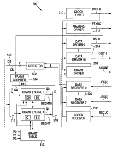
FIG. 5 shows a block diagram that illustrates an example of a bus circuit
500 of a master electronics card in accordance with the present invention. As
described in greater detail below, the bus circuit of the present invention
adaptively grants the upstream bus to the slave electronics cards in a
backplane-
based communications system by the early termination of a scheduled number of
grants to a slave electronics card when the bus circuit on the master
electronics
card detects idle cells.
In the present example, bus circuit 500 is similar to bus circuit 112C and,
as a result, utilizes the same reference numerals to designate the structures
that
are common to both circuits. As shown in FIG. 5, bus circuit 500 differs from
bus
-8
CA 02575724 2007-01-29
WO 2006/041616 PCT/US2005/033173
circuit 112C in that bus circuit 500 includes an adaptive bandwidth circuit
510 in
lieu of grant engine 224, and a grant table 512 in lieu of grant table 228.
Adaptive bandwidth circuit 510, in turn, includes a system frame counter
514 that has an input connected to receive the framing signal FSYNC from
framing driver 212, and an output. System frame counter 514 counts framing
periods, and generates a value on the output that represents either an odd
count,
or a value that represent an even count, during each framing period.
In addition, adaptive bandwidth circuit 510 includes a first grant engine GO
that generates a bus grant signal USGNTO during each even count. The bus grant
signal USGNTO identifies a slave electronics card that is to receive a bus
grant
during a next (odd) framing period of the frame synch signal FSYNC, and
transmit
data during a next (even) framing period of the frame synch signal FSYNC.
In addition, first grant engine GO includes a first consecutive counter CO
that tracks the number of consecutive times that grant engine GO has granted a
slave electronics card 112B control of the upstream bus, and a first spare
counter
SO that tracks the number of frames which were scheduled to be granted, but
which were not granted, due to the detection of idle cells.
Adaptive bandwidth circuit 510 also includes a second substantially
identical grant engine G1 that generates a bus grant signal USGNT1 during each
odd count. The bus grant signal USGNT1 identifies a slave electronics card
which
is to receive a bus grant during a next (even) framing period of the frame
synch
signal FSYNC, and transmit data during a next (odd) framing period.
Further, second grant engine G1 includes a second consecutive counter Cl
that tracks the number of consecutive times that grant engine G1 has granted a
slave electronics card 112B control of the upstream bus, and a second spare
counter S1 that tracks the number of frames which were scheduled to be
granted,
but which were not granted, due to the detection of idle cells. In the present
invention, grant engines GO and G1 are aware of the values held in each others
spare counter SO and S1.
As further shown in FIG. 5, adaptive bandwidth circuit 510 includes a
switch 516 that is connected to the first and second grant engines GO and G1,
and to frame counter 514. Switch 516 passes an idle cell detected signal DS
and
-9
CA 02575724 2007-01-29
WO 2006/041616 PCT/US2005/033173
a congestion marker detected signal CS to first grant engine GO during even
counts, and second grant engine G1 during odd counts.
Adaptive bandwidth circuit 510 further includes a switch 518 that is
connected to grant engines GO and G1, and to frame counter 514. Switch 518
passes the grant signal USGNTO from first grant engine GO to grant driver 216
during each even count. Grant driver 216 drives the grant signal received from
grant engine GO to the slave electronics cards during each odd count.
In addition, switch 518 passes the grant signal USGNT1 from second grant
engine G1 to grant driver 216 during each odd count. Grant driver 216 drives
the
grant signal received from grant engine G1 to the slave electronics cards
during
each even count. (In the example shown, switch 516 has an inverting control
input, while switch 518 has a non-inverting control input.)
In addition, adaptive bandwidth circuit 510 includes a detector circuit 522
that has an input connected to data receivers 220 to receive the data signals
USD[7:0], and an output connected to the input of switch 516. (Although only
one line is shown in FIG. 5, the one line represents a first line and a second
line
that separately carry the idle cell detected signal DS and the congestion
marker
detected signal CS, respectively.)
Grant table 512, in turn, is connected to the first and second grant engines
GO and G1 and, as shown in FIG. 5, includes a first engine pointer P0, a
second
engine pointer P1, and a next pointer P2. Table 2 illustrates an example of
grant
table 512.
Slot Number Maximum # Frames Burst Enable
2 1 No
1 10 No
3 4 Yes
5 2 No
4 20 Yes
0 25 No
Unused Entry
-10
CA 02575724 2007-01-29
WO 2006/041616 PCT/US2005/033173
Unused Entry
TABLE 2
As shown, Table 2 includes a slot number column, a maximum number of
frames column, and a burst enable column such that each listed slot number is
either burst enabled or not.
In operation, framing driver 212 outputs the frame synch signal FSYNC,
which has a plurality of framing periods, while system frame counter 514
counts
the number of framing periods to indicate a value that has an even numbered
count with a. first logic state or an odd numbered count with a second logic
state.
In frame 0 and, the succeeding even numbered frames, system frame
counter 514 outputs a switch signal SW with a logic state that allows the idle
cell
detected signal DS and the congestion marker detected signal CS to pass
through
switch 516 to grant engine GO, and the bus grant signal USGNT1 from grant
engine G1 to pass through switch 518 to grant driver 216.
In frame 1 and the succeeding odd numbered frames, frame counter 514
changes the logic state of the signal to allow the idle cell detected signal
DS and
the congestion marker detected signal CS to pass through switch 516 to grant
engine G1, and the grant signal USGNTO from grant engine GO to pass through
switch 518 to grant driver 216.
During frame 0, grant engine GO reads the slot number, the maximum
number of frames, and whether or not the slot is burst enabled from the row of
grant table 512 identified by the frst engine pointer P0. Thus, in the present
example, grant engine GO reads from row 1 that the slave electronics card
identified as slot 2 is to receive one frame.
In response, grant engine GO generates a bus grant signal USGNTO that
grants the slave electronics card identified as slot 2 control over the
upstream bus
during the next even framing period. The grant to slot 2 is held in grant
engine
GO until frame 1 arrives. In addition, grant engine GO determines that the
slave
-11
CA 02575724 2007-01-29
WO 2006/041616 PCT/US2005/033173
electronics card identified as slot 2 has received the maximum number of
frames
(one), and resets the consecutive counter C0.
Further, grant engine GO sets the first engine pointer PO to be equal to the
next frame pointer P2 which, in the present example, is equal to row 3. Grant
engine GO also sets the next frame pointer P2 to the next populated row in
grant
table 512 which, in the present example, is row 4.
During frame 1, grant driver 216 receives the bus grant signal USGNTO
from grant engine GO via switch 518, and drives the bus grant signal USGNTO as
the bus grant signal USGNT to the slave electronics cards. Further, grant
engine
G1 reads the slot number, the maximum number of frames, and whether or not
the slot is burst enabled from the row of grant table 512 identified by second
engine pointer P1. Thus, in the present example, grant engine G1 reads from
row
2 that the slave electronics card identified as slot 1 is to receive ten
frames.
In response, grant engine G1 generates a bus grant signal USGNT1 that
grants the slave electronics card identified as slot 1 control over the
upstream bus
during the next odd framing period. The grant to slot 1 is held in grant
engine G1
until frame 2 arrives. In addition, grant engine G1 adjusts the value held by
the
second engine consecutive counter Cl to indicate that a grant has been sent.
For
example, the maximum number of frames read from grant table 512 can be
stored in the second engine consecutive counter Cl, and the value can be
decremented by one since one grant has been sent.
During frame 2, the slave electronics card that is identified as slot 2
transmits upstream data signals USD[7:0] over the upstream bus to the data
receivers 220. Grant driver 216 also receives the bus grant signal USGNT1 from
grant engine Gl via switch 518, and drives the bus grant signal USGNTI as the
bus grant signal USGNT to the slave electronics cards.
In addition, grant engine GO reads the slot number, the maximum number
of frames, and whether or not the slot is burst enabled from the row of grant
table 512 identified by first engine pointer P0. Thus, in the present example,
grant engine GO reads from row 3 that the slave electronics card identified as
slot
3 is to receive 4 frames.
-12
CA 02575724 2007-01-29
WO 2006/041616 PCT/US2005/033173
In response, grant engine GO generates a grant signal USGNTO that grants
the slave electronics card connected to slot 3 control over the upstream bus
during the next even framing period. The grant to slot 3 is held in grant
engine
GO until frame 3 arrives. In addition, grant engine GO adjusts the value held
by
the first engine consecutive counter CO to indicate that a grant has been
sent.
For example, the maximum number of frames read from grant table 512 can be
stored in the first engine consecutive counter CO, and the value can be
decremented by one since one grant has been sent.
During frame 3, the slave electronics card identified as slot 1 transmits the
upstream data signals USD[7:0] to the data receivers 220. Grant driver 216
also
receives the bus grant signal USGNTO from grant engine GO via switch 518, and
drives the bus grant signal USGNTO as the bus grant signal USGNT to the slave
electronics cards.
Further, since grant engine G1 has only transmitted one of the 10 frames
allotted to the slave electronics card identified as slot 1, grant engine G1
again
generates a grant signal USGNT1 that grants the slave electronics card
identified
as slot 1 control over the upstream bus during the next odd framing period.
In addition, grant engine G1 again adjusts the value held by the second
engine consecutive counter Cl to indicate that another grant has been
generated.
For example, the value stored in the second engine consecutive counter Cl can
be again decremented by one to a value of eight since another grant has been
sent.
During frame 4, the slave electronics card identified as slot 3 transmits
upstream data signals USD[7:0] over the upstream bus to the data receivers
220.
As long as a slave electronics card has data to send, the process continues as
above with each grant engine GO and G1 counting a number of consecutive
grants that have been output to a slave electronics card that corresponds with
a
slot number, and outputting a grant signal to the slave electronics card
during
each alternating count until the number of consecutive grant signals indicates
that
the maximum number of grants have been received.
Once the number of consecutive grant signals indicates that the maximum
number of grants listed in grant table 512 have been received, the grant
engine
-13
CA 02575724 2007-01-29
WO 2006/041616 PCT/US2005/033173
moves to the next row in grant table 512 that is identified by the pointer to
grant
control of the upstream bus to another slave electronics card.
Further, in accordance with the present invention, detector 522 evaluates
the upstream data signals USD[7:0] received by receivers 220 to detect any
idle
cells within a frame and, when detected, generates the idle cell detected
signal
DS to indicate that an idle cell was detected within the frame.
When the grant engine receives the idle cell detected signal DS, the grant
engine responds as though the slave electronics circuit has received the
maximum
number of grants allowed by grant table 512, even though fewer than all of the
grants have been received. Specifically, the grant engine suspends the
remaining
grants the slave electronics card connected to the slot was scheduled to
receive,
and increases the value held in the spare counter by the number of remaining
grants.
For example, if detector circuit 522 detects an idle cell during frame 3
when the slave electronics card identified as slot 1 is transmitting, detector
circuit
522 generates the idle cell detected signal DS to indicate that an idle cell
has
been detected. Grant engine G1 responds by determining whether the number of
consecutive grants equals the maximum number of grants and, when the values
are unequal, determining a difference value.
In addition, grant engine G1 increases the value held in the second spare
counter S1 by the difference value, nine in this example since idle cells were
detected during the framing period before the second of the ten grants was
output. Thus, nine of the ten grants were spared.
After increasing the value in the spare counter, the grant engine sets the
consecutive counter to a value that indicates that the maximum number of
grants
have been received. For example, after grant engine G1 increases the value
held
in the second spare counter S1 by nine, grant engine G1 sets the second
consecutive counter C1 to zero, thereby indicating that the maximum number of
frames has been granted.
Further, the grant engine also sets the engine pointer to be equal to the
next pointer, and sets the next pointer to identify the next populated row in
the
table. For example, grant engine G1 sets the second engine pointer P1 to be
-14
CA 02575724 2007-01-29
WO 2006/041616 PCT/US2005/033173
equal to the next pointer P2 which, in the present example, is equal to row 4
(pointer P0 points to row 3 in this example). Further, grant engine G1 sets
the
next pointer P2 to identify the next populated row in the table which, in the
present example, is row 5.
Thus, in accordance with the present invention, as soon as a grant engine
receives an idle cell detected signal DS that indicates that an idle cell was
detected, the grant engine stops granting the bus to the current slave
electronics
card, even though the slave electronics card is scheduled to receive more
grants,
and moves on to grant the bus to another slave electronics card. As a result,
the
utilization efficiency of the upstream bus is substantially increased.
Thus, unlike the prior art, where a slave electronics card can continue to
receive bus grants even though there is no more data to send, the present
invention allows other slave electronics cards to receive bus grants when the
slave electronics card scheduled to receive the next grant has no more data to
send, as indicated by the presence of idle cells.
Due to conditions in a communication path, a slave electronics card, which
has a relatively low average traffic throughput, may receive a burst of ATM
cells
in a short period of time. If the throughput of the slave electronics card is
assigned a relatively low level, the data buffer in that slave electronics
card may
become full and drop cells.
In additional accordance with the present invention, when the data in a
data buffer in a slave electronics card exceeds a watermark level, the slave
electronics card can place a congestion marker in the header of each ATM cell
sent. The watermark level, in turn, indicates that the data buffer has
exceeded a
threshold level and that cells are in danger of being dropped. The slave
electronics card also removes the congestion marker when the data in the data
buffer falls below the watermark level.
In the present invention, detector circuit 522 also determines whether the
data signals USD[7:0] includes a congestion marker. When detected, detector
circuit 522 generates the congestion marker detected signal CS which passes
through multiplexer 516 to indicate to a grant engine that the congestion
marker
was detected.
-15
CA 02575724 2007-01-29
WO 2006/041616 PCT/US2005/033173
If the grant engine determines that the current slave electronics card has
additional grants to receive (only two of ten scheduled grants have been
generated), the grant engine ignores the congestion marker detected signal CS.
On the other hand, if the grant engine determines that the current slave
electronics card is being granted its last scheduled bus grant signal, the
grant
engine outputs an additional bus grant signal to the slave electronics card.
The
additional bus grant signal follows the last scheduled bus grant signal when
the
congestion marker is detected, burst mode is enabled, and a spare counter has
a
positive non-zero value that indicates that extra frames are available.
Thus, if burst mode for the slave electronics card is enabled in grant table
512, and if extra grants are available as measured by the first or the second
spare
counters SO and S1, then the grant engine sends additional bus grant signals
to
the slave electronics card when the congestion marker is detected. The
additional
bus grant signals continue until both spare counters are zero, the congestion
marker has been removed (as a result of the data falling below the watermark
level in the buffer), or idle cells are detected.
Once an additional bus grant signal has been sent, the grant engine
reduces the value of a spare counter by one. The grant engine first seeks to
reduce the value of its own spare counter, and only reduces the value of the
spare counter of the other grant engine if its own spare counter is equal to
zero.
For example, assume that the slave electronics card identified as slot 3
receives a burst of data and places a congestion marker in the header of a
cell in
the second frame of data. Since the slave electronics card identified as slot
3 is to
receive two more grants, the grant engine ignores the congestion marker
detected signal DS generated by detector 522.
On the other hand, since the burst mode for the slave electronics card is
enabled in grant table 512, and the second spare counter S1 indicates that
nine
spare grants are available, when grant engine GO detects the congestion marker
after the fourth grant has been issued to the slave electronics card
identified as
slot 3, grant engine GO sends additional bus grant signals to the slave
electronics
card identified as slot 3 until both spare counters are zero, the congestion
marker
has been removed, or idle cells are detected.
-16
CA 02575724 2007-01-29
WO 2006/041616 PCT/US2005/033173
Further, each time an additional bus grant signal is generated, grant
engine GO flrst attempts to reduce the value of the first spare counter SO. In
the
present example, the value of the first spare counter SO is equal to zero,
while the
value of the second spare counter S1 is equal to nine. Thus, since the first
spare
counter SO is equal to zero, first grant engine GO decrements the value held
by
the second spare counter S1 by one.
Each of the spare counters SO and S1 is reset to zero when the grant
engine's table pointer (PO or P1) passes the end of grant table 512. For
example,
when the table pointer PO passes the end of grant table 512, grant engine GO
resets the value held by spare counter SO to zero.
Thus, by enabling burst mode, a slave electronics circuit can request and
obtain additional grants to accommodate burst conditions if any spare grants
have
been obtained by the early termination of a number of grants that were
scheduled to be given to other slave electronics cards.
The following pseudo code further describes an example of the operation
of one grant engine.
serve_cnt = 0; //the value of the consecutive counter.
idle_det = false; //true if an idle cell is detected.
pt_det = false; //true if a congestion-marked cell is detected.
cur_slot = Null; //the current slot number.
spare_cnt = 0; //the value held by the spare counter.
1. forever {
2. wait for start of frame;
3. if (serve_cnt>0 and idle_det == false), send_grant(cur slot);
//line 3, if all of the frames scheduled to be granted to a slave electronics
card have yet to be granted and no idle cell has been detected, send the bus
grant signal USGNT to the slave electronics card in the slot currently
controlling
the upstream bus.
-17
CA 02575724 2007-01-29
WO 2006/041616 PCT/US2005/033173
4. else if (serve_cnt==0 and idle_det==false && pt det ==true &&
5. burst enable==true &&
6. (spare_cnt>0 or other_engine_spare_cnt>0)) {
7. send_grant(cur_slot);
8. if (spare_cnt>0), then spare_cnt = spare_cnt-1
9. else other engine_spare_cnt =
10. other_engine_spare_cnt-1;
11. }
//lines 4-11, if all of the frames scheduled to be granted to a slave
electronics card have been granted, no idle cell has been detected, a
congestion
condition has been detected, burst enable has been enabled, and the value held
by either of the spare counter of the two grant engines GO or G1 is greater
than
zero, send the bus grant signal USGNT to the slave electronics card in the
slot
currently controlling the upstream bus, and decrement the value of one of the
spare counters.
12. else {
13. if (next_pointer<= pointer), spare_cnt = 0; //pointer across 0
//line 13, if the next pointer is less than the current pointer for the grant
engine, then the end of the grant table has been reached and the spare counter
is
reset to zero.
14. else spare_cnt = spare_cnt + serve_cnt;
//line 14, if an idle cell is detected, set the spare count to be equal to the
spare count plus the consecutive count.
15. pointer = next_pointer
16. next pointer = get next pointer(next pointer);
17. serve_cnt = pointer[max_frame];
-18
CA 02575724 2007-01-29
WO 2006/041616 PCT/US2005/033173
18. cur slot = pointer[slot num];
19. send_grant(cur slot);
20. }
//lines 15-20, set a new value for the current slot, set the serving counter
to the maximum number of frames that can be granted to the current slot, and
send the bus grant signal USGNT to the slave electronics card in the current
slot.
21. serve_cnt = serve_cnt-1;
//reduce the serving count by one when the bus grant signal USGNT is
generated.
22. wait for start of frame;
23. idle_det = false;
24. for (i=0; i<8; i=i+1) if (idle_cell_detected) idle_det = true;
25. pt det = false;
26. for (i=0; i<8; i=i+1) if (congestion marked cell is detected)
27. pt det = true;
28. }
//at the start of a frame, set the idle cell detect and congestion detect to
false, but set to true if detected in the next eight cells.
29. get_next pointer(next pointer)
30. { new = next_pointer + 1;
31. if (new==gnum), new = 0;
32. return(new);
33. }
It should be understood that the above descriptions are examples of the
present invention, and that various alternatives of the invention described
herein
-19
CA 02575724 2007-01-29
WO 2006/041616 PCT/US2005/033173
may be employed in practicing the invention. Thus, it is intended that the
following claims define the scope of the invention and that structures and
methods within the scope of these claims and their equivalents be covered
thereby.
-20