Note: Descriptions are shown in the official language in which they were submitted.
CA 02575818 2007-01-31
WO 2006/017530 PCT/US2005/027478
STACKED ORGANIC PHOTOSENSITIVE DEVICES
Field of the Invention
[0001] The present invention generally relates to organic photosensitive
optoelectronic
devices. More specifically, it is directed to organic photosensitive
optoelectronic devices having
increased efficiency.
Background of the Invention
[0002] Optoelectronic devices rely on the optical and electronic
properties of materials to
either produce or detect electromagnetic radiation electronically or to
generate electricity from
ambient electromagnetic radiation.
[0003] Photosensitive optoelectronic devices convert electromagnetic
radiation into
electricity. -Solar cells, also called photovoltaic (PV) devices, are a type
of photosensitive
optoelectronic device that is specifically used to generate electrical power.
PV devices, which
may generate electrical energy from light sources other than sunlight, can be
used to drive power
consuming loads to provide, for example, lighting, heating, or to power
electronic circuitry or
devices such as calculators, radios, computers or remote monitoring or
communications
equipment. These power generation applications also often involve the charging
of batteries or
other energy storage devices so that operation may continue when direct
illumination from the
sun or other light sources is not available, or to balance the power output of
the PV device with a
specific application's requirements. As used herein the term "resistive load"
refers to any power
consuming or storing circuit, device, equipment or system.
[0004] Mother type of photosensitive optoelectronic device is a
photoconductor cell. In
this function, signal detection circuitry monitors the resistance of the
device to detect changes
due to the absorption of light.
CA 02575818 2007-01-31
WO 2006/017530
PCT/US2005/027478
[0005] Another type of photosensitive optoelectronic device is a
photodetector. In
operation a photodetector is used in conjunction with a current detecting
circuit which measures
the current generated when the photodetector is exposed to electromagnetic
radiation and may
have an applied bias voltage. A detecting circuit as described herein is
capable of providing a
bias voltage to a photodetector and measuring the electronic response of the
photodetector to
electromagnetic radiation.
[0006] These three classes of photosensitive optoelectronic devices may
be characterized
according to whether a rectifying junction as defined below is present and
also according to
whether the device is operated with an external applied voltage, also known as
a bias or bias
voltage. A photoconductor cell does not have a rectifying junction and is
normally operated with
- a bias. A PV device has at least one rectifying junction and is operated
with no bias. A
photodetector has at least one rectifying junction and is usually but not
always operated with a
bias. As a general rule, a photovoltaic cell provides power to a circuit,
device or equipment, but
does not provide a signal or current to control detection circuitry, or the
output of information
from the detection circuitry. In contrast, a photodetector or photoconductor
provides a signal or
current to control detection circuitry, or the output of information from the
detection circuitry but
does not provide power to the circuitry, device or equipment.
[0007] Traditionally, photosensitive optoelectronic devices have been
constructed of a
number of inorganic semiconductors, e.g., crystalline, polycrystalline and
amorphous silicon,
gallium arsenide, cadmium telluride and others. Herein the term
"semiconductor" denotes
materials which can conduct electricity when charge carriers are induced by
thermal or
electromagnetic excitation. The term "photoconductive" generally relates to
the process in
which electromagnetic radiant energy is absorbed and thereby converted to
excitation energy of
electric charge carriers so that the carriers can conduct, L e., transport,
electric charge in a
material. The terms "photoconductor" and "photoconductive material" are used
herein to refer to
semiconductor materials which are chosen for their property of absorbing
electromagnetic
radiation to generate electric charge carriers.
2
CA 02575818 2007-01-31
WO 2006/017530
PCT/US2005/027478
[0008] PV devices may be characterized by the efficiency with which they
can convert
incident solar p6v;ier to useful electric power. Devices utilizing crystalline
or amorphous silicon
dominate commercial applications, and some have achieved efficiencies of 23%
or greater.
However, efficient crystalline-based devices, especially of large surface
area, are difficult and
expensive to produce due to the problems inherent in producing large crystals
without significant
efficiency-degrading defects. On the other hand, high efficiency amorphous
silicon devices still
suffer from problems with stability. Present commercially available amorphous
silicon cells
_
have stabilized efficiencies between 4 and 8%. More recent efforts have
focused on the use of
organic photovoltaic cells to achieve acceptable photovoltaic conversion
efficiencies with
economical production costs.
[0009] PV devices may be optimized for maximum electrical power
generation under
standard illumination conditions (i.e., Standard Test Conditions which are
1000 W/m2, AM1.5
spectral illumination), for the maximum product of photocurrent times
photovoltage. The power
conversion efficiency of such a cell under standard illumination conditions
depends on the
following three parameters: (1) the current under zero bias, i.e., the short-
circuit current /sc, (2)
the photovoltage under open circuit conditions, i.e., the open circuit voltage
Voc, and (3) the fill
factor, if
[0010] PV devices produce a photo-generated current when they are
connected across a
load and are irradiated by light. When irradiated under infinite load, a PV
device generates its
maximum possible voltage, V open-circuit, or Voc. When irradiated with its
electrical contacts
shorted, a PV device generates its maximum possible current, I short-circuit,
or Isc. When
actually used to generate power, a PV device is connected to a finite
resistive load and the power
output is given by the product of the current and voltage, I xV. The maximum
total power
generated by a PV device is inherently incapable of exceeding the product, 'Sc
x Voc. When the
load value is optimized for maximum power extraction, the current and voltage
have the values,
'max and V.,,õ respectively.
[0011] A figure of merit for PV devices is the fill factor,ff, defined
as:
3
CA 02575818 2007-01-31
WO 2006/017530 PCT/US2005/027478
ff={ tri. V.. }/{ 'Sc Voc } (1)
where ff is always less than 1, as 'Sc and Voc are never obtained
simultaneously in actual use.
Nonetheless, as ff approaches 1, the device has less series or internal
resistance and thus delivers
a greater percentage of the product of Isc and Voc to the load under optimal
conditions. Where
Pine is the power incident on a device, the power efficiency of the device,
rlp, may be calculated
by:
=if* (isc * Voc) / Pine
10012] When electromagnetic radiation of an appropriate energy is
incident upon a
semiconductive organic material, for example, an organic molecular crystal
(QMC) material, or a
polymer, a photon can be absorbed to produce an excited molecular state. This
is represented
symbolically as So + hv So*. Here So and So* denote ground and excited
molecular states,
respectively. This energy absorption is associated with the promotion of an
electron from a
bound state in the HOMO energy level, which may be a 7c-bond, to the LUMO
energy level,
which may be a 7c*-bond, or equivalently, the promotion of a hole from the
LUMO energy level
to the HOMO energy level. In organic thin-film photoconductors, the generated
molecular state
is generally believed to be an exciton, i.e., an electron-hole pair in a bound
state which is
transported as a quasi-particle. The excitons can have an appreciable life-
time before geminate
recombination, which refers to the process of the original electron and hole
recombining with
each other, as opposed to recombination with holes or electrons from other
pairs. To produce a
photocurrent the electron-hole pair becomes separated, typically at a donor-
acceptor interface
between two dissimilar contacting organic thin films. If the charges do not
separate, they can
recombine in a geminant recombinatidn process, also known as quenching, either
radiatively, by
the emission of light of a lower energy than the incident light, or non-
radiatively, by the -
production of heat. Either of these outcomes is undesirable in a
photosensitive optoelectronic
device.
[0013] Electric fields or inhomogeneities at a contact may caus9 an
exciton to quench
rather than dissociate at the donor-acceptor interface, resulting in no net
contribution to the
4
CA 02575818 2007-01-31
WO 2006/017530
PCT/US2005/027478
current. Therefore, it is desirable to keep photogenerated excitons away from
the contacts. This
has the effect of limiting the diffusion of excitons to the region near the
junction so that the
associated electric field has an increased opportunity to separate charge
carriers liberated by the
dissociation of the excitons near the junction.
[0014] To produce internally generated electric fields which occupy a
substantial
volume, the usual method is to juxtapose two layers of material with
appropriately selected
-
conductive properties, especially with respect to their distribution of
molecular quantum energy
states. The interface of these two materials is called a photovoltaic
heterojunction. In traditional
semiconductor theory, materials for forming PV heterojunctions have been
denoted as generally
being of either n or p type. Here n-type denotes that the majority carrier
type is the electron.
This could be viewed as the material having many electrons in relatively free
energy states. The
p-type denotes that the majority carrier type is the hole. Such material has
many holes in
relatively free energy states. The type of the background, i.e., not photo-
generated, majority
carrier concentration depends primarily on unintentional doping by defects or
impurities. The
type and concentration of impurities determine the value of the Fermi energy,
or level, within the
gap between the highest occupied molecular orbital (HOMO) energy level and the
lowest
unoccupied molecular orbital (LUMO) energy level, called the HOMO-LUMO gap.
The Fermi
energy characterizes the statistical occupation of molecular quantum energy
states denoted by the
value of energy for which the probability of occupation is equal to 1A. A
Fermi energy near the
LUMO energy level indicates that electrons are the predominant carrier. A
Fermi energy near
the HOMO energy level indicates that holes are the predominant carrier.
Accordingly, the Fermi
energy is a primary characterizing property of traditional semiconductors and
the prototypical
PV heterojunction has traditionally been the p-n interface.
- [0015] The term "rectifying" denotes, inter alia, that an interface
has an asymmetric
conduction characteristic, i.e., the interface supports electronic charge
transport preferably in one
direction. Rectification is associated normally with a built-in electric field
which occurs at the
heterojunction between appropriately selected materials.
CA 02575818 2007-01-31
WO 2006/017530 PCT/US2005/027478
[0016] As used herein, and as would be generally understood by one
skilled in the art, a
first "Highest Occupied Molecular Orbital" (HOMO) or "Lowest Unoccupied
Molecular
Orbital" (LUMO) energy level is "greater than" or "higher than" a second HOMO
or LUMO
energy level if the first energy level is closer to the vacuum energy level.
Since ionization
potentials (IP) are measured as a negative energy relative to a vacuum level,
a higher HOMO
energy level corresponds to an IP having a smaller absolute value (an IP that
is less negative).
Similarly, a higher LUMO energy level corresponds to an electron affinity (EA)
having a smaller
absolute value (an EA that is less negative). On a conventional energy level
diagram, with the
vacuum level at the top, the LUMO energy level of a material is higher than
the HOMO energy
level of the same material. A "higher" HOMO or LUMO energy level appears
closer to the top
of such a diagram than a "lower" HOMO or LUMO energy level.
[0017] In the context of organic materials, the terms "donor" and
"acceptor" refer to the
relative positions of the HOMO and LUMO energy levels of two contacting but
different organic
materials. This is in contrast to the use of these terms in the inorganic
context, where "donor"
and "acceptor" may refer to types of dopants that may be used to create
inorganic n- and p- types
layers, respectively. In the organic context, if the LUMO energy level of one
material in contact
with another is lower, then that material is an acceptor. Otherwise it is a
donor. It is
energetically favorable, in the absence of an external bias, for electrons at
a donor-acceptor
junction to move into the acceptor material, and for holes to move into the
donor material.
[0018] A significant property in organic semiconductors is carrier
mobility. Mobility
measures the ease with which a charge carrier can move through a conducting
material in
response to an electric field. In the context of organic photosensitive
devices, a layer including a
material that conducts preferentially by electrons due to a high electron
mobility may be referred
to as an electron transport layer, or ETL. A layer including a material that
conducts
preferentially by holes due to a high hole mobility may be referred to as a
hole transport layer, or
HTL. Preferably, but not necessarily, an acceptor material is an ETL and a
donor material is a
HTL.
[0019] Conventional inorganic semiconductor PV cells employ a p-n
junction to establish
6
CA 02575818 2007-01-31
WO 2006/017530 PCT/US2005/027478
an internal field. Early organic thin film cells, such as reported by Tang,
AppL Phys Lett. 48, 183
(1986), contain a heterojunction analogous to that employed in a conventional
inorganic PV cell.
However, it is now recognized that in addition to the establishment of a p-n
type junction, the
energy level offset of the heterojunction also plays an important role.
[0020] The energy level offset at the organic D-A heterojunction is
believed to be
important to the operation of organic PV devices due to the fundamental nature
of the
_
photogeneration process in organic materials. Upon optical excitation of an
organic material,
localized Frenkel or charge-transfer excitons are generated. For electrical
detection or current
generation to occur, the bound excitons must be dissociated into their
constituent electrons and
holes. Such a process can be induced by the built-in electric field, but the
efficiency at the
electric fields typically found in organic devices (F 106 V/cm) is low. The
most efficient
exciton dissociation in organic materials occurs at a donor-acceptor (D-A)
interface. At such an
interface, the donor material with a low ionization potential forms a
heterojunction with an
acceptor material with a high electron affinity. Depending on the alignment of
the energy levels
of the donor and acceptor materials, the dissociation of the exciton can
become energetically
favorable at such an interface, leading to a free electron polaron in the
acceptor material and a
free hole polaron in the donor material.
[0021] Organic PV cells have many potential advantages when compared to
traditional
silicon-based devices. Organic PV cells are light weight, economical in
materials use, and can
be deposited on low cost substrates, such as flexible plastic foils. However,
some organic PV
devices typically have relatively low external quantum efficiency, being on
the order of 1 % or
less. This is, in part, thought to be due to the second order nature of the
intrinsic
photoconductive process. That is, carrier generation requires exciton
generation, diffusion and
ionization or collection. There is an efficiency ri associated with each of
these processes.
Subscripts may be used as follows: P for power efficiency, EXT for external
quantum efficiency,
A for photon absorption, ED for exciton diffusion, CC for charge collection,
and INT for internal
quantum efficiency. Using this notation:
rip nEXT = 11A *liED * 11CC
7
CA 02575818 2012-07-10
75655-26
riEXT = 11A* niNT
[0022] The diffusion length (LD) Of an exciton is typically much less
(L9 ¨ 50A) than the
optical abso0 tion length (-500A:), requiring a trade off between using a
thick, and therefore
resistive, cell with multiple or highly folded interfaces, or a thin cell with
a low optical
abso0 tion efficiency.
10023] Typically, when light is absorbed to form an exciton in an
organic thin film, a
singlet exciton is formed. By the mechanism of intersystem crossing, the
singlet exciton may
decay to a triplet exciton. In this process energy is lost which will result
in a lower efficiency for
the device. If not for the energy loss from intersystem crossing, it would be
desirable to use
materials that generate triplet excitons, as triplet excitons generally have a
longer lifetime, and
therefore a longer diffusion length, than do singlet excitons.
Summary of the Invention
[0024] A device is provided having a first electrode, a second
electrode, a first
photoactive region having a characteristic absorption wavelength Xi and a
second photoactive
region having a characteristic absorption wavelength k2. The photoactive
regions are disposed
between the first and second electrodes, and further positioned on the same
side of a reflective
layer, such that the first photoactive region is closer to the reflective
layer than the second
photoactive region. The materials comprising the photoactive regions may be
selected such that
Al is at least about 10% different from X2. The device may further comprise an
exciton blocking
layer disposed adjacent to and in direct contact with the organic acceptor
material of each
photoactive region, wherein the LUMO of each exciton blocking layer other than
that closest to
the cathode is not more than about 0.3 eV greater than the LUMO of the
acceptor material.
8
CA 02575818 2012-07-10
75655-26
[0024a] According to another aspect of the present invention, there is
provided
a device, comprising: an anode; a cathode; a plurality of stacked organic
photoactive
regions, disposed between and electrically connected to the anode and the
cathode,
each organic photoactive region further comprising an organic acceptor
material and
an organic donor material; and an exciton blocking layer provided in at least
two of
the plurality of stacked organic photoactive regions, each exciton blocking
layer being
disposed adjacent to and in direct physical contact with the organic acceptor
material
of each organic photoactive region, wherein a LUMO of each exciton blocking
layer
other than the exciton blocking layer closest to the cathode is not more than
about
0.3 eV greater than a LUMO of the acceptor material.
Brief Description of the Drawings
[0025] Figure 1 shows an organic PV device comprising an anode, an
anode
smoothing layer, a donor layer, an acceptor layer, a blocking layer, and a
cathode.
[0026] Figure 2 shows an organic tandem device formed by stacking two
cells
in series.
8a
CA 02575818 2007-01-31
WO 2006/017530 PCT/US2005/027478
[0027] Figure 3 shows the optical field intensities at A, = 450 nm (solid
line) and = 650
urn (dashed line) as a function of the distance from the cathode in the
asymmetric organic
tandem cell B (see Table I), the structure of which is schematically shown at
the top of Figure 3.
[0028] Figure 4 shows the calculated external quantum efficiency spectra
for the front
(dashed line) and back (solid line) cell of cell B.
[0029] Figure 5 shows the current density vs. voltage (J¨V)
characteristics of the
asymmetric organic tandem cell A, in the dark and under various intensities of
simulated
AM1.5G solar illumination.
[0030] Figure 6 shows the illumination intensity (Po) dependence of the
power
conversion efficiencies (1k) of asymmetric organic tandem cells (A, filled
squares; B, open
circles; C, filled triangles) under simulated AM1.5G solar illumination,
compared with that of
the 5% single CuPc/C60 hybrid planar-mixed heterojunction cell (open inverted
triangles).
[0031] Figure 7 shows the fill factor (FF) of the tandem and single
hybrid PM-HJ cells
shown in Figure 6.
[0032] Figure 8 shows two possible geometries of a PV device with
representative
perpendicular optical path lengths.
[0033] Figure 9 shows absorption spectra of CuPc:C60 films with various
mixture ratios,
deposited on ITO.
Detailed Description
[0034] An organic photosensitive optoelectronic device is provided.
Organic devices of
embodiments of the present invention may be used, for example, to generate a
usable electrical
current from incident electromagnetic radiation (e.g., PV devices) or may be
used to detect
9
CA 02575818 2007-01-31
WO 2006/017530 PCT/US2005/027478
incident electromagnetic radiation. Embodiments of the present invention may
comprise an
anode, a cathode, and a photoactive region between the anode and the cathode.
The photoactive
region is the portion of the photosensitive device that absorbs
electromagnetic radiation to
generate excitons that may dissociate in order to generate an electrical
current. Organic
photosensitive optoelectronic devices may also include at least one
transparent electrode to allow
incident radiation to be absorbed by the device. Several PV device materials
and configurations
are described in U.S. Patent Nos. 6,657,378, 6,580,027, and 6,352,777, which
are incorporated
herein by reference in their entirety.
[0035] Figure 1 shows an organic photosensitive optoelectronic device
100. The figures
are not necessarily drawn to scale. Device 100 may include a substrate 110, an
anode 115, an
anode smoothing layer 120, a donor layer 125, an acceptor layer 130, a
blocking layer 135, and a
cathode 140. Cathode 140 may be a compound cathode having a first conductive
layer and a
second conductive layer. Device 100 may be fabricated by depositing the layers
described, in
order. Charge separation may occur predominantly at the organic heterojunction
between donor
layer 125 and acceptor layer 130. The built-in potential at the heterojunction
is determined by
the HOMO-LUMO energy level difference between the two materials contacting to
form the
heterojunction. The HOMO-LUMO gap offset between the donor and acceptor
materials
produce an electric field at the donor/acceptor interface that facilitates
charge separation for
excitons created within an exciton diffusion length of the interface.
[0036] The specific arrangement of layers illustrated in Figure 1 is
exemplary only, and
is not intended to be limiting. For example, some of the layers (such as
blocking layers) may be
omitted. Other layers (such as reflective layers or, additional acceptor and
donor layers) may be
added. The order of layers may be altered. Arrangements other than those
specifically described
may be used.
[0037] The substrate may be any suitable substrate that provides desired
structural
properties. The substrate may be flexible or rigid, planar or non-planar. The
substrate may be
transparent, translucent or opaque. Plastic and glass are examples of
preferred rigid substrate
materials. Plastic and metal foils are examples of preferred flexible
substrate materials. The
CA 02575818 2007-01-31
WO 2006/017530
PCT/US2005/027478
material and thickness of the substrate may be chosen to obtain desired
structural and optical
properties.
[0038] US Patent No. 6,352,777, incorporated herein by reference,
provides examples of
electrodes, or contacts, that may be used in a photosensitive optoelectronic
device. When used
herein, the terms "electrode" and "contact" refer to layers that provide a
medium for delivering
photo-generated current to an external circuit or providing a bias voltage to
the device. That is,
an electrode, or contact, provides the interface between the active regions of
an organic
photosensitive optoelectronic device and a wire, lead, trace or other means
for transporting the
charge carriers to or from the external circuit. In a photosensitive
optoelectronic device, it is
desirable to allow the maximum amount of ambient electromagnetic radiation
from the device
exterior to be admitted to the photoconductively active interior region. That
is, the
electromagnetic radiation must reach a photoconductive layer(s), where it can
be converted to
electricity by photoconductive absorption. This often dictates that at least
one of the electrical
contacts should be minimally absorbing and minimally reflecting of the
incident electromagnetic
radiation. That is, such a contact should be substantially transparent. The
opposing electrode
may be a reflective material so that light which has passed through the cell
without being
absorbed is reflected back through the cell. As used herein, a layer of
material or a sequence of
several layers of different materials is said to be "transparent" when the
layer or layers permit at
least 50% of the ambient electromagnetic radiation in relevant wavelengths to
be transmitted
through the layer or layers. Similarly, layers which permit some, but less
that 50% transmission
of ambient electromagnetic radiation in relevant wavelengths are said to be
"semi-transparent."
[0039] -As used herein, "top" means furthest away from the substrate,
while "bottom"
means closest to the substrate. For example, for a device having two
electrodes, the bottom
electrode is the electrode closest to the substrate, and is generally the
first electrode fabricated.
The bottom electrode has two surfaces, a bottom surface closest to the
substrate, and a top
surface further away from the substrate. Where a first layer is described as
"disposed over" a
second layer, the first layer is disposed further away from substrate. There
may be other layers
\ between the first and second layer, unless it is specified that the first
layer is "in physical contact
11
CA 02575818 2007-01-31
WO 2006/017530 PCT/US2005/027478
with" the Second layer. For example, a cathode may be described as "disposed
over" an anode,
even though there are various organic layers in between.
[0040] The electrodes are preferably composed of metals or "metal
substitutes". Herein
the term "metal" is used to embrace both materials composed of an elementally
pure metal, e.g.,
Mg, and also metal alloys which are materials composed of two or more
elementally pure metals,
e.g., Mg and Ag together, denoted Mg:Ag. Here, the tenn "metal substitute"
refers to a material
that is not a metal within the normal definition, but which has the metal-like
properties that are
desired in certain appropriate applications. Commonly used metal substitutes
for electrodes and
charge transfer layers would include doped wide-bandgap semiconductors, for
example,
transparent conducting oxides such as indium tin oxide (ITO), gallium indium
tin oxide (GITO),
and zinc indium tin oxide (ZITO). In particular, ITO is a highly doped
degenerate n+
semiconductor with an optical bandgap of approximately 3.2 eV, rendering it
transparent to
wavelengths greater than approximately 3900 A. Another suitable metal
substitute is the
transparent conductive polymer polyanaline (RANI) and its chemical relatives.
Metal substitutes
may be further selected from a wide range of non-metallic materials, wherein
the term "non-
metallic" is meant to embrace a wide range of materials provided that the
material is free of
metal in its chemically uncombined form. When a metal is present in its
chemically uncombined
form, either alone or in combination with one or more other metals as an
alloy, the metal may
alternatively be referred to as being present in its metallic form or as being
a "free metal". Thus,
the metal substitute electrodes of the present invention may sometimes be
referred to as "metal-
free" wherein the term "metal-free" is expressly meant to embrace a material
free of metal in its
chemically uncombined form. Free metals typically have a form of metallic
bonding that results
from a sea of valence electrons which are free to move in an electronic
conduction band
throughout the metal lattice. While metal substitutes may contain metal
constituents they are
"non-metallic" on several bases. They are not pure free-metals nor are they
alloys of free-
metals. When metals are present in their metallic form, the electronic
conduction band tends to
provide, among other metallic properties, a high electrical conductivity as
well as a high
reflectivity for optical radiation.
12
CA 02575818 2007-01-31
WO 2006/017530 PCT/US2005/027478
=
[0041] Embodiments of the present invention may include, as one or more
of the
transparent electrodes of the photosensitive optoelectronic device, a highly
transparent, non-
metallic, low resistance cathode such as disclosed in U.S. Patent No.
6,420,031, to Parthasarathy
et al. ("Parthasarathy '031"), or a highly efficient, low resistance
metallic/non-metallic
compound cathode such as disclosed in U.S. Patent No. 5,703,436 to Forrest et
al. ("Forrest
'436"), both incorporated herein by reference in their entirety. Each type of
cathode is preferably
prepared in a fabrication process that includes the step of sputter depositing
an ITO layer onto
either an organic material, such as copper phthalocyanine (CuPc), to form a
highly transparent,
non-metallic, low resistance cathode or onto a thin Mg:Ag layer to form a
highly efficient, low
resistance metallic/non-metallic compound cathode.
[0042] Herein, the term "cathode" is used in the following manner. In a
non-stacked PV
device or a single unit of a stacked PV device under ambient irradiation and
connected with a
resistive load and with no externally applied voltage, e.g, a PV device,
electrons move to the
cathode from the photo-conducting material. Similarly, the term "anode" is
used herein such that
in a PV device under illumination, holes move to the anode from the photo-
conducting material,
which is equivalent to electrons moving in the opposite manner. It will be
noted that as the terms
are used herein, anodes and cathodes may be electrodes or charge transfer
layers.
[0043] An organic photosensitive device will comprise at least one
photoactive region in
which light is absorbed to form an excited state, or "exciton", which may
subsequently dissociate
in to an electron and a hole. The dissociation of the exciton will typically
occur at the
heteroj unction formed by the juxtaposition of an acceptor layer and a donor
layer. For example,
in the device of Figure 1, the "photoactive region" may include donor layer
125 and acceptor
layer 130.
[0044] The acceptor material may be comprised of, for example, perylenes,
naphthalenes,
fullerenes or nanotubules. An example of an acceptor material is 3,4,9,10-
perylenetetracarboxylic bis-benzimidazole (PTCBI). Alternatively, the acceptor
layer may be
comprised of a fullerene material as described in U.S. Patent No. 6,580,027,
incorporated herein
by reference in its entirety. Adjacent to the acceptor layer, is a layer of
organic donor-type
13
CA 02575818 2007-01-31
WO 2006/017530 PCT/US2005/027478
m4terial.. The boundary of the acceptor layer and the donor layer forms the
heterojunction which
may produce an internally generated electric field. The material for the donor
layer may be a
pthalocyanine or a porphyrin, or a derivative or transition metal complex
thereof, such as copper
pthalocyanine (CuPc). Other suitable acceptor and donor materials may be used.
[0045] Through the use of an organometallic material in the photoactive
region, devices
incorporating such materials may efficiently utilize triplet excitons. It is
believed that the
singlet-triplet mixing may be so strong for organometallic compounds, that the
absorptions
involve excitation from the singlet ground states directly to the triplet
excited states, eliminating
the losses associated with conversion from the singlet excited state to the
triplet excited state.
The longer lifetime and diffusion length of triplet excitons in comparison to
singlet excitons may
allow for the use of a thicker photoactive region, as the triplet excitons may
diffuse a greater
distance to reach the donor-acceptor heterojunction, without sacrificing
device efficiency.
Materials other than organometallics may also be used.
[0046] In a preferred embodiment of the invention, the stacked organic
layers include
one or more exciton blocking layers (EBLs) as described in U.S. Patent No.
6,097,147, Peumans
et al, Applied Physics Letters 2000, 76, 2650-52, and co-pending application
serial number
09/449,801, filed Nov. 26, 1999, both incorporated herein by reference. Higher
internal and
external quantum efficiencies have been achieved by the inclusion of an EBL to
confine
photogenerated excitons to the region near the dissociating interface and to
prevent parasitic
exciton quenching at a photosensitive organic/electrode interface. In addition
to limiting the
volume over which excitons may diffuse, an EBL can also act as a diffusion
barrier to substances
introduced during deposition of the electrodes. In some circumstances, an EBL
can be made
t thick enough to fill pinholes or shorting defects which could otherwise
render an organic PV
device non-functional. An EBL can therefore help protect fragile organic
layers from damage
produced when electrodes are deposited onto the organic materials.
[0047] It is believed that the EBLs derive their exciton blocking
property from having a
LUMO-HOMO energy gap substantially larger than that of the adjacent organic
semiconductor
from which excitons are being blocked. Thus, the confined excitons are
prohibited from existing
14
CA 02575818 2007-01-31
WO 2006/017530 PCT/US2005/027478
in ;the EBL due to energy considerations. While it is desirable for the EBL to
block excitons, it is
not desirable for the EBL to block all charge. However, due to the nature of
the adjacent energy
levels, an EBL may- block one sign of charge carrier. By design, an EBL will
exist between two
other layers, usually an organic photosensitive semiconductor layer and a
electrode or charge
transfer layer. The adjacent electrode or charge transfer layer will be in
context either a cathode
or an anode. Therefore, the material for an EBL in a given position in a
device will be chosen so
that the desired sign of carrier will not be impeded in its transport to the
electrode or charge
transfer layer. Proper energy level alignment ensures that no barrier to
charge transport exists,
preventing an increase in series resistance. For example, it is desirable for
a material used as a
cathode side EBL to have a LUMO energy level closely matching the LUMO energy
level of the
adjacent ETL material so that any undesired barrier to electrons is minimized.
[0048] It should be appreciated that the exciton blocking nature of a
material is not an
intrinsic property of its HOMO-LUMO energy gap. Whether a given material will
act as an
exciton blocker depends upon the relative HOMO and LUMO energy levels of the
adjacent
organic photosensitive material. Therefore, it is not possible to identify a
class of compounds in
isolation as exciton blockers without regard to the device context in which
they may be used.
However, with the teachings herein one of ordinary skill in the art may
identify whether a given
material will function as an exciton blocking layer when used with a selected
set of materials to
construct an organic PV device.
[0049] In a preferred embodiment of the invention, an EBL is situated
between the
acceptor layer and the cathode. A preferred material for the EBL comprises 2,9-
dimethy1-4,7-
dipheny1-1,10-phenanthroline (also called bathocuproine or BCP), which is
believed to have a
LUMO-HOMO energy level separation of about 3.5 eV, or bis(2-methy1-8-
hydroxyquinolinoato)-aluminum(III)phenolate (A1q2OPH). BCP is an effective
exciton blocker
which can easily transport electrons to the cathode from an acceptor layer.
[0050] The EBL layer may be doped with a suitable dopant, including but
not limited to
3,4,9,10-perylenetracarboxylic dianhydride (PTCDA), 3,4,9,10-
perylenetracarboxylic diimide
(PTCDI), 3,4,9,10-perylenetetracarboxylic-bis-benzimidazole (PTCBI), 1,4,5,8-
CA 02575818 2007-01-31
WO 2006/017530 PCT/US2005/027478
naphthalenetetracarboxylic dianhydiide (NTCDA), and derivatives thereof. It is
thought that the
BCP as deposited in the present devices is amorphous. The present apparently
amorphous BCP
exciton blocking layers may exhibit film recrystallization, which is
especially rapid under high
light intensities. The resulting morphology change to polycrystalline material
results in a lower
quality film with possible defects such as shorts, voids or intrusion of
electrode material.
Accordingly, it has been found that doping of some EBL materials, such as BCP,
that exhibit this
effect with a suitable, relatively large and stable molecule can stabilize the
EBL structure to
prevent performance degrading morphology changes. It should be further
appreciated that
doping of an EBL which is transporting electrons in a giving device with a
material having a
LUMO energy level close to that of the EBL will help insure that electron
traps are not formed
which might produce space charge build-up and reduce performance.
Additionally, it should be
appreciated that relatively low doping densities should minimize exciton
generation at isolated
dopant sites. Since such excitons are effectively prohibited from diffusing by
the surrounding
EBL material, such absorptions reduce device photoconversion efficiency.
[0051] Representative embodiments may also comprise transparent charge
transfer layers
or charge recombination layers. As described herein charge transfer layers are
distinguished
from acceptor and donor layers by the fact that charge transfer layers are
frequently, but not
necessarily, inorganic (often metals) and they may be chosen not to be
photoconductively active.
The term "charge transfer layer" is used herein to refer to layers similar to
but different from
electrodes in that a charge transfer layer only delivers charge carriers from
one subsection of an
optoelectronic device to the adjacent subsection. The term "charge
recombination layer" is used
herein to refer to layers similar to but different from electrodes in that a
charge recombination
layer allows for the recombination of electrons and holes between tandem
photosensitive devices
and may also enhance internal optical field strength near one or more active
layers. A charge
recombination layer can be constructed of semi-transparent metal nanoclusters,
nanoparticle or
nanorods as described in U.S. Patent No. 6,657,378, incorporated herein by
reference in its
entirety.
[0052] In a preferred embodiment of the invention, an anode-smoothing
layer is situated
between the anode and the donor layer. A preferred material for this layer
comprises a film of
16
CA 02575818 2007-01-31
WO 2006/017530 PCT/US2005/027478
3,4-polyeihylenedioxythiophene:polystyrenesulfonate (PEDOT:PSS). The
introduction of the
PEDOT:PSS layer between the anode (ITO) and the donor layer (CuPc) may lead to
greatly
improved fabrication yields. This is attributed to the ability of the spin-
coateid PEDOT:PSS film
to planarize the ITO, whose rough surface could otherwise result in shorts
through the thin
molecular layers.
[0053] In a further embodiment on the invention, one or more of the
layers may be
treated with plasma prior to depositing the next layer. The layers may be
treated, for example,
with a mild argon or oxygen plasma. This treatment is beneficial as it reduces
the series
resistance. It is particularly advantageous that the PEDOT:PSS layer be
subject to a mild plasma
treatment prior to deposition of the next layer.
[0054] The simple layered structure illustrated in Figure 1 is provided
by way of non-
limiting example, and it is understood that embodiments of the invention may
be used in
connection with a wide variety of other structures. The specific materials and
structures
described are exemplary in nature, and other materials and structures may be
used. Functional
devices may be achieved by combining the various layers described in different
ways, or layers
may be omitted entirely, based on design, performance, and cost factors. Other
layers not
.specifically described may also be included. Materials other than those
specifically described
may be used. Although many of the examples provided herein describe various
layers as
comprising a single material, it is understood that combinations of materials,
such as a mixture of
host and dopant, or more generally a mixture, may be used. Also, the layers
may have various
sublayers. The names given to the various layers herein are not intended to be
strictly limiting.
Organic layers that are not a part of the photoactive region, i.e., organic
layers that generally do
not absorb photons that make a significant contribution to photocurrent, may
be referred to as
"non-photoactive layers." Examples of non-photoactive layers include EBLs and
anode-
smoothing layers. Other types of non-photoactive layers may also be used.
[0055] Preferred organic materials for use in the photoactive layers of a
photosensitive
device include cyclometallated organometallic compounds. The term
"organometallic" as used
herein is as generally understood by one of ordinary skill in the art and as
given, for example, in
17
CA 02575818 2007-01-31
WO 2006/017530 PCT/US2005/027478
"Inorganic Chemistry" (2nd Edition) by Gary L. Miessler and Donald A. Tarr,
Prentice Hall
(1998). Thus, the term organometallic refers to compounds which have an
organic group bonded
to a metal through a carbon-metal bond. This class does not include per se
coordination
compounds, which are substances having only donor bonds from heteroatoms, such
as metal
complexes of amines, halides, pseudohalides (CN, etc.), and the like. In
practice organometallic
compounds generally comprise, in addition to one or more carbon-metal bonds to
an organic
species, one or more donor bonds from a heteroatom. The carbon-metal bond to
an organic
species refers to a direct bond between a metal and a carbon atom of an
organic group, such as
phenyl, alkyl, alkenyl, etc., but does not refer to a metal bond to an
"inorganic carbon," such as
the carbon of CN or CO. The term cyclometallated refers to compounds that
comprise an
bidentate organometallic ligand so that, upon bonding to a metal, a ring
structure is formed that
includes the metal as one of the ring members.
[0056] Organic layers may be fabricated using vacuum deposition, spin
coating, organic
vapor-phase deposition, inkjet printing and other methods known in the art.
[0057] Organic photosensitive optoelectronic devices may function as a
PV,
photodetector or photoconductor. Whenever the organic photosensitive
optoelectronic devices
of the present invention function as a PV device, the materials used in the
photoconductive
organic layers and the thicknesses thereof may be selected, for example, to
optimize the external
quantum efficiency of the device. Whenever the organic photosensitive
optoelectronic devices
= of the present invention function as photodetectors or photoconductors,
the materials used in the
photoconductive organic layers and the thicknesses thereof may be selected,
for example, to
maximize the sensitivity of the device to desired spectral regions.
[00581 This result may be achieved by considering several guidelines that
may be used in
the selection of layer thicknesses. It is desirable for the exciton diffusion
length, LD, to be
greater than or comparable to the layer thickness, L, since it is believed
that most exciton
dissociation will occur at an interface. If LD is less than L, then many
excitons may recombine
before dissociation. It is further desirable for the total photoconductive
layer thickness to be of
the order of the electromagnetic radiation absorption length, 1/a (where a is
the absorption
18
=
CA 02575818 2007-01-31
WO 2006/017530 PCT/US2005/027478
coefficient), so that nearly all of the radiation incident on the PV device is
absorbed to produce
excitons. Furthermore, the photoconductive layer thickness should be as thin
as possible to
avoid excess series resistance due to the high bulk resistivity of organic
semiconductors.
10059] Accordingly, these competing guidelines inherently require
tradeoffs to be made
in selecting the thickness of the photoconductive organic layers of a
photosensitive
optoelectronic cell. Thus, on the one hand, a thickness that is comparable or
larger than the
absorption length is desirable (for a single cell device) in order to absorb
the maximum amount
of incident radiation. On the other hand, as the photoconductive layer
thickness increases, two
undesirable effects are increased. One is that due to the high series
resistance of organic
semiconductors, an increased organic layer thickness increases device
resistance and reduces
efficiency. Another undesirable effect is that increasing the photoconductive
layer thickness
increases the likelihood that excitons will be generated far from the
effective field at a charge-
separating interface, resulting in enhanced probability of geminate
recombination and, again,
reduced efficiency. Therefore, a device configuration is desirable which
balances between these
competing effects in a manner that produces a high external quantum efficiency
for the overall
device.
[0060] The organic photosensitive optoelectronic devices of the present
invention may
function as photodetectors. In this embodiment, the device may be a multilayer
organic device,
for example as described in U.S. Application Serial No. 10/723,953, filed
November 26, 2003,
.incorporated herein by reference in its entirety. In this case an external
electric field may be
generally applied to facilitate extraction of the separated charges.
[0061] A concentrator or trapping configuration can be employed to
increase the
efficiency of the organic photosensitive optoelectronic device, where photons
are forced to make
multiple passes through the thin absorbing regions. U.S. Patent Nos. 6,333,458
and 6,440,769,
incorporated herein by reference in their entirety, addresses this issue by
using structural designs
that enhance the photoconversion efficiency of photosensitive optoelectronic
devices by
optimizing the optical geometry for high absorption and for use with optical
concentrators that
increase collection efficiency. Such geometries for photosensitive devices
substantially increase
19
CA 02575818 2007-01-31
WO 2006/017530 PCT/US2005/027478
the, optical path through the material by trapping the incident radiation
within a reflective cavity
or waveguiding structure, and thereby recycling light by multiple reflection
through the
photoresponsive material. The geometries disclosed in U.S. Patent Nos.
6,333,458 and
6,440,769 therefore enhance the external quantum efficiency of the devices
without causing
substantial increase in bulk resistance. Included in the geometry of such
devices is a first
reflective layer; a transparent insulating layer which should be longer than
the optical coherence
length of the incident light in all dimensions to prevent optical microcavity
interference effects; a
transparent first electrode layer adjacent the transparent insulating layer; a
photosensitive
heterostructure adjacent the transparent electrode; and a second electrode
which is also
reflective.
[0062] Coatings may be used to focus optical energy into desired regions
of a device. US
Patent Application No. 10/857,747, which is incorporated by reference in its
entirety, provides
examples of such a coating.
[0063] The power conversion efficiency (1k) of organic cells may be
improved through
the use of new materials and the introduction of novel device structures. The
efficiency of
organic cells may be improved by using the acceptor material C60 with a long
exciton diffusion
length (LD r-z-; 400A), or by forming a bulk heterojunction structure, where
an interpenetrating
network of donor and acceptor materials enhances tlie probability of excitons
diffusing to a
nearby, "local" D¨A interface. One embodiment of the present invention
provides a copper
phthalocyanine (CuPc)/C60 organic cell incorporating a hybrid planar-mixed
heterojunction (PM-
Hi), consisting of a mixed D¨A layer sandwiched between homogeneous donor and
acceptor
layers. The device demonstrates Tip -= 5% under simulated AM1.5G solar
illumination.
[0064] Stacking two or more cells in series is one way to harvest more
photons while
increasing the open-circuit voltage (Voc) of the cell. A more than doubling of
individual
CuPc/PTCBI cell efficiencies of rip = 1% to tip = 2.5% has been demonstrated,
as described in
A. YakimoV and S. R. Forrest, Appl. Phys. Lett. 80, 1667 (2002), by stacking
two thin cells in
series, with Ag nanoclusters between the subcells providing both optical field
enhancement and
efficient recombination sites for the photogenerated charges. The photovoltage
of this "tandem"
CA 02575818 2007-01-31
WO 2006/017530 PCT/US2005/027478
cell may be twice that of each individual cell (or subcell). One embodiment of
the present
invention comprises two CuPc/C60 hybrid PM-HJ cells in series, with each cell
having a different
ratio of CuPc to Co. This configuration results in rip = (5.7 0.3)% under 1
sun = 100 mW/cm2
simulated AM1.5G solar illumination, representing ¨15% increase from a single
hybrid PM-HJ
cell. Also, Voc of the tandem cell is greater than that of a single PV cell,
reaching up to about
1.2 V under high intensity illumination. One embodiment of the present
invention employs the
highly efficient material combination of CuPc and Cgo in hybrid planar-mixed
double
heterojunction structures. Without including antireflection coatings on the
substrates, organic PV
cells with solar power conversion efficiencies of 6.5% may be possible using
tandem structures
of this type.
[0065] A two-subcell CuPc/PTCBI tandem cell has symmetric spectral
response from
each of the two subcells. The optical interference between the incident light
and that reflected
from the metal cathode leads to a maximum optical intensity at a perpendicular
optical path
length of X/4 from the organic/cathode interface, where X is the incident
light wavelength. As
used herein, "perpendicular optical path length" refers to distance/n,
measured normal to the
surface of the device and integrated over the path traveled by light, where n
is the index of
refraction of the material and may vary within the material. Hence, an
"asymmetric" tandem cell
with a front cell rich in long-wavelength absorbing molecules, and a back cell
rich in short-
wavelength absorbing molecules, may absorb more incident light than an
otherwise equivalent
tandem cell having equal mixtures of CuPc and Cgo in each subcell. For
example, if CuPc
absorbs between X = 550 urn and 750 run, and Cgo between X = 350 nm and 550
nm, an
asymmetric CuPc/C60 hybrid PM-HJ tandem cell may include a front cell with a
thicker
homogeneous CuPc layer and a thinner Cgo layer than the back cell. A tradeoff
between the
homogeneous and mixed layer thicknesses may also be used to balance the
photocurrent in the
two subcells, due to the short exciton diffusion lengths in the homogeneous
layers and the low
charge mobilities in the mixed layers.
[0066] The efficiency of a CuPc/C60 hybrid PM-HJ tandem cell may be
maiximized by
modeling the current density vs. voltage (J¨V) characteristics of subcell i (i
= 1,2 denoting the
front and back cell, respectively) following:
21
CA 02575818 2007-01-31
WO 2006/017530 PCT/US2005/027478
Ji (v.) = fd,i(Vi)+ J Ph,i(V exP i)= J.0
{ [q(V; ¨ J , Rs,i )]
nikT 1}+J Tl (V)
Pki .CC,i i ,
(1)
where Jczi and JPh,t are the dark and photo current densities, respectively,
Jo is the reverse-bias
saturation current, ni is the ideality factor, Rs, i is the cell series
resistance, q is the electron
charge, k is Boltzmann's constant, and T is the temperature. Using a model
that considers both
optical interference and exciton diffusion, the photocurrent density Jõ,,
under an incident optical
power density Po may be obtained, assuming all photogenerated charges are
collected at the
electrodes. This assumption may not hold for a cell with a mixed layer, where
charge carrier
mobilities are significantly reduced from those in homogeneous layers due to
molecular
intermixing, leading to recombination of photogenerated charges within the
mixed layer. The
charge collection efficiency ricc, or the proportion of charges collected at
the electrodes, as a
function of the applied voltage V and the mixed layer thickness din is
Tlcc (V) = c
L (V)
{1 ex[ dc in
, (2)
L (11]}
where LcOl= La(Vbi ¨V)IV is the charge collection length, La is a constant,
and Vbi is the
built-in potential. Given Ji = Ji(V;) (i = 1,2), the J¨V characteristics of
the tandem cell are
obtained from the requirement that J = J1 = J2, and V = Vi + V2, from which
the PV cell
performance parameters (short-circuit current density Jsc, open-circuit
voltage Voc, fill factor
FF, and power conversion efficiency rip) are obtained.
[00671
Table 1 provides the device structures of three tandem cells. Table 2
summarizes
the parameter values used in the model. Referring to Table 1, cell A has mixed
layer thicknesses
based on given asymmetric homogeneous layer thicknesses, leading to rip = 5.2%
under 1 sun
AM1.5G solar illumination. The combination of photoactive layer thicknesses in
cell B leads to a
higher efficiency of rip = 5.9%. A PTCBI layer in the front cell may also
contribute to the
photocurrent when the front-cell homogeneous C60 layer is removed, so that
CuPc molecules in
the-mixed layer may form an exciton dissociation interface with PTCBI. This
leads to a higher
Jsc and a maximum lip = 6.5% in cell C, as the PTCBI absorption fills the gap
between the
absorption regions of CuPc and C60, at around k = 550 urn.
22
CA 02575818 2012-07-10
75655-26
TABLE 1.
Cell Front cell Back cell Jsc Voc FF
label
CuPc CUPC:C60 C60 PTCBI CuPc CUPC:C60 C60 BCP (mA/cn1 9 (V)
(0/0)
A 100 180 20 50 20 130 250 75 9.4 1.03 0.54
5.2
B 75 125 80 50 60 130 160 75 9.7 1.03
0.59 5.9
90 110 0 50 50 100 210 100 10.3 1.04 0.61 6.5
TABLE 2.
Rsn LoVbi LD (A)
(nA/cm2) (Q-cm2) (A) (V) CuPc C60 PTCBI
35 0.25 1.6 400 0.65 80 400 30
=
[0068] In one embodiment of the invention, photoactive regions are
disposed between
two electrodes. In preferred embodiments of the invention, the photoactive
regions comprise
hybrid planar-mixed heterojunction (PM-HJ) devices, as described in US Patent
Application No.
10/822774, incorporated herein by reference in its entirety.
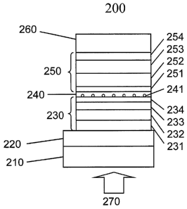
[0069] Figure 2 shows an organic photoactive device 200 according to
one embodiment
of the invention. Device 200 may comprise a substrate 210 on which is
deposited a first
electrode 220, a first (or "front") organic photoactive region 230, an
intervening layer 240, a
second (or "back") photoactive region 250, and a second electrode 260. The
organic photoactive
regions 230 and 250 comprise an organic acceptor material and an organic donor
material.
23
CA 02575818 2012-07-10
75655-26
In another preferred embodiment of the invention, the second photoactive
region 250 comprises
a similar embodiment of the invention, the second photoactive region 250
comprises a similar
arrangement of organic materials as first photoactive region 230. In a
preferred embodiment of
the invention, intervening layer 240 comprises a charge recombination zone. In
another
preferred embodiment, intervening layer 240 may comprise one or more
electrodes, where
multiple electrodes may be separated by an insulating layer.
[0070] In another embodiment of the present invention, the mixture of
the organic
acceptor material and the organic donor material in a mixed organic layer,
such as organic layer
232 may occur in a ratio ranging from about 10:1 to about 1:10 by weight,
respectively. In one
embodiment, an organic layer including a mixture of acceptor and donor
materials (such as
organic layer 232), and an organic layer that includes only an acceptor
material or a donor
material (such as second organic layer 23 1 or 233) may be present.
[0071] When an EBL is deposited in a layer adjacent to and in direct
contact with a
deposited cathode, the EBL may be damaged. This damage is believed to be
advantageous in
that it may allow charge carriers to pass across the EBL more easily, while
still preventing
excitons from doing so. It is believed that selecting materials for the EBL
and organic acceptor
layers such that the LUMO of each EBL is not more than about 0.3 eV greater
than the LUMO
of the adjacent acceptor material produces a similar result. To obtain
favorable charge transport
properties, it is therefore preferable that an EBL disposed adjacent to an
acceptor layer is (1) not
separated from the second electrode by a photoactive region; and/or (2) has a
LUMO not more
than about 0.3 eV greater than the LUMO of an adjacent photoactive region. If
a particular EBL
is not separated from the second electrode by a photoactive region, such that
the EBL is subject
to damage during deposition of the second electrode, the LUMO difference
between the EBL
and the acceptor is less important and the criteria used to select the EBL
material may be
weighted more towards factors other than LUMO.
24
CA 02575818 2007-01-31
WO 2006/017530 PCT/US2005/027478
[0072] In a preferred embodiment of the device, the second exciton
blocking layer 254
comprises a different material than the first exciton blocking layer 234.
Because exciton
blocking layer 254 is not separated from the second electrode by a photoactive
region, a broader
selection of materials may be available. The material of exciton blocking
material 254 may have
a LUMO of not more than about 0.3 eV greater than the LUMO of organic acceptor
layer 253, or
it may have a LUMO that is greater, bt charge transport may still be favorable
due to damage
caused by the deposition of the second electrode 260. Preferred materials for
exciton blocking
layer 254 include BCP, and preferred materials for exciton blocking layer 234
include PTCBI.
[0073] In another embodiment of the invention, organic cell 200 further
comprises an
intervening layer 240. Intervening layer 240 may comprise a charge
recombination zone. In a
preferred embodiment of the invention, the charge recombination zone comprises
a p-doped
organic material, such as m-MTDATA:F4-TCNQ or BTQBT:PTCDA, and the charge
recombination zone further comprises nanoparticles 241. It is especially
preferred that the
nanoparticles comprise Ag or another metal or metallic material. Other
materials may be used.
[0074] In a tandem cell, it may be advantageous to use different acceptor
and donor
materials, or the same acceptor and donor materials in different ratios, in
each subcell. Using
different materials or different ratios of the same materials may allow the
cell to absorb light in a
greater range of wavelengths than if the same materials in the same ratios are
used in each
subcell. In a preferred embodiment of the invention, organic regions 230 and
250 comprise
different acceptor and donor materials. Organic regions 230 and 250 may also
comprise the
same acceptor and donor materials, wherein the mixed organic layers 232 and
252 comprise
different ratios of the acceptor and donor materials. The organic acceptor
material of organic
regions 230 and 250 may be Co. The organic donor material of photoactive
regions 230 and 250
may be CuPc. Other suitable organic donor materials include lead
phthalocyanine (PbPc), metal
containing porphyrins, metal-free porphyrins, rubrene, metal containing
phthalocyanines, metal-
free phthalocyanines, diamines (such as NPD), and fiinctionalized variants
thereof, including =
naphthalocyanines.. Other suitable organic acceptor materials include PTCBI,
C70, fullerenes,
perylenes, catacondensed conjugated molecular systems such as linear
polyacenes (including
anthracene, napthalene, tetracene, and pentacene), pyrene, coronene, and
functionalized variants
CA 02575818 2007-01-31
WO 2006/017530 PCT/US2005/027478
thereof. this listing is not meant to be comprehensive, and other suitable
acceptor and donor
materials may be used.
[0075] In an especially preferred embodiment of the present invention,
the anode
comprises a transparent, conducting indium-tin-oxide (ITO) layer on a glass
substrate, and the
cathode comprises a 1000 A thick thermally evaporated Ag electrode. The
photoactive region of
each subcell comprises a hybrid PM-HJ, i.e., a mixed CuPc:C60 layer disposed
between
homogeneous CuPc and C60 layers, which combines the advantages of a planar HJ
between
homogeneous layers (good transport of photogenerated charge carriers to their
respective
electrodes) and a mixed layer (high exciton diffusion efficiency). A thin
layer of 3,4,9,10-
perylenetetracarboxylic bis-benzimidazole (PTCBI) and bathocuproine (BCP) is
used as the
exciton-blocking layer (EBL) in the front (nearest the ITO) and back (nearest
the cathode)
subcells, respectively, thereby forming a high efficiency double
heterojunction PV structure. A
charge recombination zone for electrons generated in the front cell and holes
generated in the
back cell is disposed between the subcells. The recombination centers comprise
Ag nanoclusters
deposited in an ultrathin (-5A, average thickness) layer disposed in a 50 A
thick 4,4',4"-tris(3-
methyl-phenyl-phenyl-amino)friphenylamine (m-MTDATA) p-doped with 5 mol%
tetrafluoro-
tetracyano-quinodimethane (F4-TCNQ). Device fabrication procedures and methods
of
characterization may be those known in the art.
[0076] It is understood that the embodiments described herein are
exemplary only, and
that other embodiments may be used in accordance with the present invention.
For example, the
order of the layers illustrated may be altered. For example, the positions of
the organic layers 230
and 250 may be switched, with appropriate repositioning of blocking layers,
etc. Additional
layers may or may not also be present, such-as blocking layers, charge
recombination layers, etc.
For example, blocking layers may be removed, and / or additional blocking
layers may be
present. Non-organic regions may be present, and may be used to adjust the
position of the
organic regions relative to a reflecting layer. Different materials than those
specifically
described may be used. For example, a device where all of the electrodes are
ITO may be
fabricated such that the device may be transparent to some degree.
Additionally, the device
could be fabricated onto a substrate, and then applied to a supporting
surface, such that the last
26
CA 02575818 2007-01-31
WO 2006/017530 PCT/US2005/027478
electrode'deposited is closest to the supporting surface. Acceptor and donor
layers may not be
present. For example, donor or acceptor layers 231, 251, 233, and 253 may be
absent. Although
many embodiments are described with respect to solar cells, other embodiments
may be used in
other types of devices, such as a photodetector.
[0077] Where a layer is described as an "unmixed" acceptor or donor
layer, the
"unmixed" layer may include very small amounts of the opposite material as an
impurity. A
material may be considered an impurity if the concentration is significantly
lower than the
amount needed for percolation in the layer, i.e., less than about 5% by
weight. Preferably, any
impurity is present in a much lower amount, such as less than 1% by weight or
most preferably
less than about 0.1% by weight. Depending upon the processes and process
parameters used to
fabricate devices, some impurities of the materials in immediately adjacent
layers may be
unavoidable.
[0078] Organic materials may have absorption spectra with maxima at
specific
wavelengths. As used herein, the term "characteristic absorption wavelength"
refers to the
wavelength at which the absorption spectrum of a material has a maximum.
[0079] Device 200 may include at least one reflective layer. In one
embodiment of the
invention, second electrode 260 is a reflective layer. Other configurations
may be used, such as
the use of a separate reflective layer, or a top emitting (or absorbing)
device where the substrate
or the first electrode is the reflective layer. A "reflective" layer may be a
metal layer, or another
type of layer that reflects, such as an aperiodic or periodic dieliectric
stack. The use of a
reflective layer leads to an optical field strength that varies with
wavelength and with position in
a direction perpendicular to the reflective layer. For any given wavelength,
there are maxima in
the optical field strength as a function ofposition. See, for example, Figure
3. For
photosensitive devices, it is desirable to locate a photoactive region having
a particular
characteristic absorption wavelength such that the position having a maximum
as a function of
position for that wavelength is located within or near the photoactive region.
For a photoactive
region having multiple materials, the characteristic absorption wavelength is-
based on the
maxima of the absorption spectra of the entire region. "Near" may mean, for
example, at a
distance that is not more than about .05X/n from the photoactive region in
question, where n is
27
CA 02575818 2007-01-31
WO 2006/017530 PCT/US2005/027478
the index of refraction of the material in which the maximum occurs.
Preferably, the maximum
is disposed within the photoactive region. Locating the photoactive region in
this manner will
lead to enhanced absorption. For some applications, it is desirable to use
light absorbing regions
that have significantly different characteristic absorption wavelengths. Such
a difference may
allow for absorption of a broader range of wavelengths. In one embodiment of
the invention,
organic regions 250 and 230 have characteristic absorption wavelengths at Xi
and X2,
respectively. It is preferred that ki be at least about 10% different from X2.
Characteristic
absorption wavelength is only one way of quantifying "different" absorption
spectra. Another
way of quantifying different absorption spectra is that the wavelength of at
least one of the top
three absorption peaks of one photoactive region is at least 10% different
from all of the
wavelengths of the top 3 absorption peaks of another photoactive region. Yet
another way to
quatify different absorption spectra is to superimpose two normalized spectra
on each other, and
to measure the area that overlaps. It this overlap area is 80% or less of the
total area of one of
the spectra, the spectra can be considered significantly different. For
example, two materials
may have similar characteristic absorption wavelengths, but other features
(such as subpeaks)
that are significantly different, and possibly complementary for purposes of
absorbing a broad
spectra of incident light. Such an embodiment is intended to be within the
scope of certain
aspects of the invention.
[0080] Many photoactive materials (and combinations of materials, for
photoactive
regions having multiple materials) may have a plurality of absorption peaks. A
photoactive
region that strongly absorbs a particular wavelength of light may be placed at
a position where
the optical field strength for that wavelength is strong. In one embodiment, a
local peak in the
absorption spectra of a photoactive region is used to determine a favorable
position for the
photoactive region. The photoactive region may be located at or near a maximum
in the optical
field intensity for the wavelength for which the photoactive region has a
local maximum. For
devices intended to absorb the solar spectrum, wavelengths between 350 and
1300 nm may be of
greater importance. In general terms, it is preferable to increase or maximixe
the overlap of
optical field intensity at a particular wavelength or range of wavelengths
with a photoactive
region that is a strong absorber of those wavelengths. One way to achieve this
is adjusting the
position of a photoactive region towards a position where there is a greater
overlap between the
absorption of the photoactive region and the optical field intensity (both as
functions of
28
CA 02575818 2007-01-31
WO 2006/017530 PCT/US2005/027478
wavelength). Another way is to alter the absorption characteristics of a
photoactive region by
altering the materials therein, or the ratio of materials, to achieve a
greater overlap between the
absorption spectrum and the optical field intensity (both as functions of
wavelength) at the
position of the photoactive region.
100811 One way to describe such a match is to determine the wavelength of
the top 3
absorption peaks for a photoactive region, and place the photoactive region
such that a peak in
the optical field strength for one of these three wavelengths is either in the
photoactive region or
within .057in of the photoactive region, where k is the wavelength of the peak
that matches the
maximum in the optical field strength, and n is the index of refraction of the
layer in which the
peak in the optical field intensity is located. Another way to describe such a
match is to consider
the wavelengths of all of the absorption peaks of the photoactive region(s).
The "wavelength" of
an absorption peak is the local maximum of the absorption spectra for the
peak, and the "top
three" peaks are the peaks having the three highest local maximums. When
determining the
"top" wavelength or wavelengths, the wavelength range may be limited in some
embodiments.
For example, for some devices intended to absorb the solar spectrum, the range
of wavelength
considered may be limited to 350 - 1300 urn because a large fraction of the
usable energy of the
solar spectra falls within this range, although broader ranges may also be
used in some
embodiments, including embodiments intended to absorb the solar spectrum.
[0082] Locating photoactive regions as described may lead to an increase
in the amount
of incident light absorbed. In preferred embodiments of the invention,
materials and positions of
the photoactive regions are selected such that at least about 10%, and more
preferably at least
about 20%, of the total incident electric field intensity is located in a
photoactive region having
absorption characteristics such that the energy may be absorbed. As used
herein, "optical field
intensity" refers to the integral of the square of the electric field over a
region. Thus, the total
incident electric field intensity is the integral of the square of the
electric field over the entire
device, and the total electric field of the photoactive regions is the sum of
the electric field
integrated over each of the photoactive regions. Thus, for a region R, the
intensity IR will be
calculated as:
/R = 11E12
29
CA 02575818 2007-01-31
WO 2006/017530 PCT/US2005/027478
as, will be appreciated by one skilled in the art. Moreover, the optical field
intensity at each point
is also a function of wavelength. It is preferred to increase the integral as
a function of position
over the photoactive regions of the device of: the integral over wavelength of
the product of the
absorption characteristic of the photoactive region (which may be a function
of position and
wavelength) with the optical field intensity (which may also be a function of
both position and
wavelength). This quantity, divided by the total optical field intensity, is
the percentage of
optical field intensity that may be absorbed by the device, and which is
preferably at least 10%,
and more preferably at least 20%. The percentage of optical field intensity
that may be absorbed
may be increased, for example, by selecting materials that are good absorbers
of particular
wavelengths of light, and placing them where the optical field intensity for
that particular
wavelength is great. It is believed that this will lead to increased
absorption by the photoactive
regions, and thus an improved efficiency of the device. In a preferred
embodiment, the optical
field intensity is based upon a solar spectrum. Note that peak matching may
not be the only way
to achieve 10% or 20% as described above. Matching photoactive regions that
have strong
absorption at a particular wavelength (regardless of whether there is a peak)
with a strong value
for that wavelength in the optical field intensity is one such way to
accomplish this goal. By
calculating the integral described above, it is possible to determine whether
a device will have
strong absorption or not.
[0083] For the case of a single reflective layer, which is a good
approximation of many
embodiments, there is a maximum in the optical field strength for a particular
wavelength X at an
optical path length X /4 distant from the reflective layer. Hence, it is
further preferred that at
least a portion of the first photoactive region 250 is disposed at a
perpendicular optical path
length about 2i/4 25% from the edge of the reflective layer closest to the
first photoactive
region, and at least a portion of the second photoactive region 230 is
disposed at a perpendicular
optical path length about ?2/4 25% from the edge of the reflective layer
closest to the second
photoactive region, where Xi and X2 are the wavelengths at which the first and
second
photoactive regions are strong absorbers. A "strong absorber" may be
quantified in a number of
ways. In one embodiment, the wavelength of at least one of the absorption
peaks of the second
photoactive region may be greater than the wavelength of at least one of the
absorption peaks of
= the first photoactive region. In another embodiment, the wavelength of at
least one of the top
three absorption peaks of the second photoactive region may be greater than
the wavelength of at
=
CA 02575818 2007-01-31
WO 2006/017530 PCT/US2005/027478
least one Of the top three absorption peaks of the first photoactive region.
The 25% margin is a
measure of how far the wavelength of the absorption peak may be from the
maximum in the
optical field strength, while still maintaining a significant overlap between
a strong optical field
strength and a strong absorption for that wavelength and nearby avelengths.
More generally, for
the case of a single reflective layer and configurations that have a similar
optical field intensity
profile, it is preferred to place longer wavelength absorbing materials
proportionally farther from
the reflecting surface than shorter wavelength absorbing materials, where the
constant of
proportionality is X / n, where n is the index of refraction of the materials
in the stack. Where n
varies throughout the stack, a spatially weighted mean index of refraction of
the materials
comprising the stack may be used. For more complex optical configurations, one
of skill in the
art, with the benefit of this disclosure, will be able to determine the
location of maxima in the
optical field strength.
[0084] While many embodiments of the invention are described with respect
to two
stacked cells, it is understood that a greater number of stacked cells may be
used, and the
concepts relating to positioning the cells and the blocking layers used
adjacent to the cells are
generally applicable to stacks having more than two cells.
[0085] As used herein, and as would be understood by one skilled in the
art, the term
"blocking layer" means that the layer provides a barrier that significantly
inhibits transport of
charge carriers and/or excitons through the device, without suggesting that
the layer necessarily
completely blocks the charge miners and/or excitons. The presence of such a
blocking layer in a
device may result in substantially higher efficiencies as compared to a
similar device lacking a
blocking layer.
[0086] Figure 3 shows the optical field intensities at X = 450 nm (solid
line) and X = 650
inn (dashed line) as a function of the distance from the cathode in the
asymmetric organic
tandem cell B (see Table I), whose structure is shown schematically at the top
of Figure 3. The
intensity at X = 450 nin peaks at approximately 400 A from the reflecting Ag
cathode, or about
300 A closer than that for X = 650 nm. Hence, making the front cell rich in
shorter wavelength
absorbing material(s) and the back cell rich in lower wavelength absorbing
material(s) may lead
to increased absorption of a broad spectrum. In cell B the back cell has a
significantly thicker
31
CA 02575818 2007-01-31
WO 2006/017530 PCT/US2005/027478
homogeneous Cgo layer than the front cell, leading to a higher external
quantum efficiency in the
Cgo absorption region (X <550 urn), as shown in Figure 4. As the light
intensity at X ==-=,' 650 urn is
primarily located in the front cell, the quantum efficiency at 550 nm <A <750
nm may be higher
for the front cell, although the thicknesses of the homogeneous CuPc and the
mixed layers are
approximately the same in both subcells to balance their photocurrents.
[00871 Figure 4 shows the calculated external quantum efficiency spectra
for the front
(dashed line) and back (solid line) cell of cell B. The asymmetric spectral
responses from the two
subcells result from the asymmetric tandem cell structure as well as the
optical interference.
100881 Figure 5 shows the current density vs. voltage (J¨J1)
characteristics of the
asymmetric organic tandem cell A, in the dark and under various intensities of
simulated
AM1.50 solar illumination. The experimental J¨V characteristics of tandem cell
A in the dark
and under various intensities of simulated AM1.5G solar illumination are shown
(open symbols).
A rectification ratio of 105¨ 106 at 1.5 V is typical. The open-circuit
voltage is Voc = 1.04 V
under 1 sun illumination, and approaches 1.2 V under 10 suns, which may be
twice of that of a
single CuPc/C60 hybrid PM-HJ cell. The solid lines are modeled J¨V
characteristics, which
agrees with the experimental data except for the reverse-bias dark current, in
which case
generation-recombination current or thermally assisted tunneling may
significantly contribute to
41.
[0089] Figure 6 shows the measured illumination intensity (Po) dependence
of the power
conversion efficiencies (rip) of various asymmetric organic tandem cells (A,
filled squares; B,
open circles; C, filled triangles) under simulated AM1.5G solar illumination,
compared with that
of a 5% single CuPc/C60 hybrid planar-mixed heterojunction cell (open inverted
triangles). The
power conversion efficiency of tandem cell A (filled squares), derived from
the experimental J¨
V characteristics in Figure 5, reaches a maximum of lip = (5.4 0.3)% at Po =
0.34 suns. Under
higher intensity illumination, the FF decreases (see Figure 7) due to the
relatively thick mixed
layers. With thinner mixed layers, tandem cell B (open circles) exhibits a
high FF = 0.56 even
under an intense illumination of approximately 11 suns. This leads to rip =
(5.7 0.3)% at P 1
sun, in agreement with the model. However, tandem cell C (filled triangles)
has a lower
32
CA 02575818 2007-01-31
WO 2006/017530 PCT/US2005/027478
efficiency than model prediction (6.5%), mainly due to a low FF 0.51. This may
suggest a
small energy barrier at the C60/PTCBI interface impeding electrons
transporting to the charge
recombination zone. Nevertheless, the efficiencies of tandem cells A and B are
higher than the
5% single CuPc/C60 hybrid PM-HJ cell (open inverted triangles in Figure 6),
demonstrating the
effectiveness of stacking cells.
[0100] Figure 7 shows the fill factor (FF) of the tandem and single
hybrid PM-HJ cells
shown in Figure 6. Under higher intensity illumination, the FF decreases due
to the relatively
thick mixed layers. With thinner mixed layers, tandem cell B (open circles)
exhibits a high FF =
0.56 even under an intense illumination of approximately 11 suns.
101011 Figure 8 shows two possible geometries of a PV device 810 and 820,
with
representative perpendicular optical path lengths 815 and 825. The
perpendicular optical path
length is measured normal to the surface of the device.
10102] Figure 9 shows absorption spectra of CuPc:C60 films with various
mixture ratios,
deposited on ITO. The concentrations of CuPc in mixed films are 100% CuPc(CuPc
single
layer) 910, 62% 920, 40% 930, 33% 940 and 21% 950. The pure CuPc film has two
peaks
centered at wavelengths of 620 nm and 695 nm. The longer wavelength peak is
due to molecular
Frenkel exciton generation, whereas the shorter wavelength feature is
attributed to the formation
of CuPc aggregates. The longer wavelength peak is dominant in the gas phase or
dilute solution.
Figure 9 shows that the magnitude of the longer wavelength peak increases with
increasing C60
content. Accordingly, CuPc molecules show a lower tendency to aggregate with
increasing C60
content. This suggests that an increase in C60 concentration inhibits CuPc
aggregation, thereby
reducing hole transport in the mixed film, perhaps leading to a low carrier
collection efficiency.
This is reflected in the reduced power efficiency Op = (2.6 0.1) %, see
Table 2) of a CuPc:C60
(1:2) mixed layer PV cell. However, at a concentration of 1:1, there is
sufficient aggregation of
CuPc molecules to allow for low resistance hole transport, while the much
higher symmetry C60
molecules may also form a percolation path for efficient electron transport to
the cathode.
[0103] Table 1 shows the layer thicknesses (in A) of three organic tandem
photovoltaic
cells as well as predicted performance parameters (short-circuit current
density Js, open-circuit
33
CA 02575818 2007-01-31
WO 2006/017530 PCT/US2005/027478
voltage Voc, fill factor FF, and power conversion efficiency Tip) under 1 sun
AM1.5G solar
illumination. The charge recombination zone in each tandem cell consists of a
5 A thick Ag
nanoclusters layer and a 50 A thick m-MTDATA doped with 5 mol% F4-TCNQ.
10104] Table 2 shows the parameters used in modeling the J¨V
characteristics of
CuPc/C60 hybrid PM-HJ tandem PV cells.
[0105] It is understood that the embodiments described herein are
exemplary only, and
that other embodiments may be used in accordance with the present invention.
For example, the
order of the layers illustrated may be altered. For example, in Figures 1 and
2, the positions of
the photoactive layers, i.e., organic regions 230 and 250 may be switched,
with appropriate
repositioning of blocking layers, etc. Additional layers may or may not also
be present, such as
blocking layers, charge recombination layers, etc. For example, blocking
layers may be
removed, and / or additional blocking layers may be present. Non-photoactive
regions may be
present, and may be used to adjust the position of the photoactive regions
relative to a reflecting
layer. Various solar cell configurations may be used, such as tandem solar
cells. Different
materials than those specifically described may be used. For example, a device
where all of the
electrodes are ITO may be fabricated such that the device may be transparent
to some degree.
Additionally, the device could be fabricated onto a substrate, and then
applied to a supporting
surface, such that the last electrode deposited is closest to the supporting
surface. Although
many embodiments are described with respect to solar cells, other embodiments
may be used in
other types of photosensitive devices having a D-A heterojunction, such as a
photodetector.
101061 The power efficiencies achieved by embodiments of the invention
are higher than
previous efficiencies achieved for organic solar cells. These results may be
due to interactions
between several features of embodiment of the invention, including the use of
an unmixed,
organic photoactive layer in connection with a mixed organic photoactive
layer, with thicknesses
and positions selected with efficiency in mind. Embodiments of the invention
may be capable of
reaching power conversion efficiencies approaching that of a-Si cells,
currently in production,
with efficiencies of 7%-10%. It is expected that with refinement of devices
consistent with
embodiments of the invention, even higher power efficiencies may be achieved.
For example, by
applying simple anti-reflection coatings to the glass substrates, an
additional 10% improvement
34
CA 02575818 2007-01-31
WO 2006/017530
PCT/US2005/027478
to pfficiericies may be possible, suggesting that the tandem cell structure
proposed here may
attain efficiencies in excess of 7%. Stacking more than two cells in series
could help to harvest
more light, although an efficient cell structure is more difficult to achieve.
An ultimate
advantage of the asymmetric tandem cell structure is that it enables the
incorporation of different
donor-acceptor material combinations in the individual subcells to cover a
broader solar
spectrum region than the current CuPc¨C60 system. Provided that high
production yields and
long operational lifetimes are possible in properly packaged organic solar
cell modules, the
asymmetric hybrid PM-HJ tandem cell has considerable potential for use a
variety of
applications.
Examples
101071 In one embodiment of the invention, an efficient photovoltaic
cell is provided. A
cell with two stacked hybrid planar-mixed heterojunction cells was fabricated
on a glass
substrate pre-coated with transparent conducting ITO. The device has the
structure: ITO / 75 A
CuPc / 122 A CuPc:C60 (1.2:1 by weight)! 80 A C60 / 50 A PTCBI / 5 A Ag! 50 A
m-
- MTDATA:F4-TCNQ / 60 A CuPc / 132 A CuPc:C60 (1.2:1 by weight)! 160 A C60
/ 75 A BCP /
Ag. The cell farther away from the cathode is slightly rich in CuPc, which
absorbs in the
spectral region from 550 nm to 750 urn, whereas the cell closer to the cathode
is rich in C60,
which absorbs in the spectral region from 350 nm to 550 nm. A maximum power
efficiency was
measured of (5.6 0.3)% under 1 to 4 suns simulated AM1.5G solar
illumination.
[0108] The organic hybrid planar-mixed heterojunetion photovoltaic
cells were
fabricated on glass substrates precoated with a ¨1500 A thick transparent,
conducting ITO anode
with a sheet resistance of 15 0/Sq. The substrates were cleaned in solvent
followed by UV-ozone
treatment for 5 minutes. The organic layers and a metal cathode were deposited
via thermal
evaporation in a high vacuum chamber with a base pressure ¨ 2x1027 Ton. A CuPc
layer with a
thickness of dp ¨ 50 ¨ 200 A, a cordeposited layer of CuPc:C60 (1:1 by weight)
with a thickness
of d,n ¨ 0 ¨ 300 A, and a C60 layer with a thickness of dA ¨ 250 ¨ 400 A, are
sequentially
deposited onto the ITO anode, followed by a 100 A thick exciton-blocking layer
of BCP. Finally,
_
a 1000 A thick Ag cathode was evaporated through a shadow mask with 1 mm
diameter
openings.
CA 02575818 2007-01-31
WO 2006/017530 PCT/US2005/027478
101091 Current-voltage characteristics of the PV cells at 25 C in the
dark and under
simulated AM1.5G solar illumination from a 150 W Xe-arc lamp (Oriel
Instruments) were
measured using an HP 4155B semiconductor parameter analyzer. The illumination
intensity was
varied using neutral density filters and measured with a calibrated broadband
optical power
meter (Oriel Instruments).
[ono'. Although the present invention is described with respect to
particular examples -
and preferred embodiments, it is understood that the present invention is not
limited to these
examples and embodiments. The present invention as claimed may therefore
include variations
from the particular examples and preferred embodiments described herein, as
will be apparent to
one of skill in the art.
36