Note: Descriptions are shown in the official language in which they were submitted.
CA 02575913 2007-02-02
WO 2006/013396 PCT/GB2005/050124
1
Ioii Mobility S ectrometer
FIELD OF THE INVENTION
The presezlt inveiition relates to aii ion iziobility spectroineter, and more
particularly to a field asyiliilictric ion mobility (FArM) spectrometer.
Certain aspects of
the invention relate to a micro macliined FAIM spectrometer. Aspects of tlle
illvention
also relate to metllods of perforiiiing ion mobility spectron3etry, and to
compolleilts for
use in such a spectroiiieter.
BACKGROUND TO THE INVENTION
Ion mobility spectrometry is a versatile tecllilique used to detect presence
of
molecular species in a gas san--ple. The technique has particular application
in detection
of explosives, drLigs, and chemical agents in a sailiple, altliottgh it is not
limited to these
applications. Portable detectors are commonly used for security screening, and
in the
defence iiidListry. However, coiiveiltioaial portable devices are still
noiletlleless relatively
large.
Ion mobility spectroiiietry relies on the differential nlovernent of different
ioil
species through an electric field to a detector; by appropriate selection of
the pararneters
of the electric field, ioils Ilaviilg differing properties will reacll the
detector at differiilg
tinles, if at all. Time of flight (TOF) ion I71oIUIlity spectrometry
I?leaslires the time taltell
by ions when subject to an electric field to travel aloilg a drift tube to a
detector against
a drift gas flow. By varying the electric field ions of different
cllaracteristics will reach
tlie detector at differeilt times, and the composition of a sample can be
analysed. This
foiiii of spectrometry relies on the length of the drift tiiue for its
resolZition; lhe longer
the drift tube, the il-iore powerft2l the detector. This restricts the
possible illiiiiaturisatioil.
of sltcll spectrometers, since there is a limit to the lower size of the drift
hiUe whicll may
effectively be used. Fui-tller, given that relatively high electric field
strengtlis are
necessary, the restriction on drifi tube length also results in the need to
use relatively
CA 02575913 2007-02-02
WO 2006/013396 PCT/GB2005/050124
7
liigll voltages in the device, which niay be potentially hazardous to the
operator and
fur-tlier restricts the possibility of miniaturisation of the device.
A variation on TOF ion nlobility spectrometry is described in US 5,789,745,
which nlakes use of a nioving electrical potential to move ions against a
drift gas flow
towards a detector. A pltirality of spaced electrodes are altenlately pulsed
to generate a
moving potential well, whicll carries selected ions along with it. Tilis
device is unsuited
to nllnlattlrlsatlon dlle to, amoiig other reasons, the need for a pump to
produce the drift
gas flow.
Field asyllimetric ion mobility spectronietry (FAIMS) is a derivative of time
of
fligllt ion mobility spectrometry (TOFIMS), which potentially offers a
snlaller fornl.
factor; however, existing desigiis use nloving gas flows and lligll voltages,
whicll are
undesirable for rrticrocl7ip inlplementations. Scaling is further liindered by
tlzolectilar
drfftision, an effect that becomes sigtli.Ocant in the micron regime.
Background
inforniation relating to FAIMs can be fotind in L.A. Buryalcov et aI. Int.J.
Mass.
Spectrom. Ion Process. 128 (1993) 143; and E.V. K.a.-ylov et al. Int.J. Mass.
Spectrom.
Ion Process. 225 (2003) 39-51; llereby incotporated by reference.
Conventional FAIMS operates by drawing air at atnlasplleric pressure into a
reaction region wliere the constituents of the saniple are ionized. Cllemical
agents in
vapotir-phase compotinds fon-i1 ion cltisters when tlley are exposed to their
parent ions.
The mobility of the ion clusters is mainly a fiislction of'sllape and weigllt,
The iotls are
blown between two nietal electrodes, one witll a low-voltage DC bias and the
other witll
a periodic lligll-voltage pulse waveform, to a detector plate where they
collide and a
culTent is registered. Ions are quickly driven toward one electrode during the
pulse
phase and slowly driven toward the opposite electrode between pulses. Some
ions
impact an electrode before reaciling the detector plate; other ions with the
appropriate
differential mobility reach the end, mal.ijig this device a sort of
differential mobility ion
filter. A plot of the ctirrent generated versus DC bias provides a
cllaracteristic
differential ioil inobility spectrtrtM. The intensity of the pealcs in the
spectrLiin, wllicll
cot-t'esponds to the aniount of charge, indicates the relative concentration
of tl-ie agent.
While this ai-rangenzent offers the possibility for greater miniattirisation
tllan
conventional TOFIMS, the need to generate a gas flow requires the presence of
a ptiznp,
diaphragiii or similar, which iising present tecllnology limits tlle lower
size of such a
CA 02575913 2007-02-02
WO 2006/013396 PCT/GB2005/050124
3
device. Representative exa~i-iples of sucla devices are described in US
6,495,823 and US
6,512,224.
It would be of benefit to provide miiliaturised ion naobility spectrometers
for use
in sensing teclu3iclues; iiot taixly would these be suitable for covert use or
for large scale
distribution, the smaller size will allow use of lower voltages in the device.
Devices
with no or fewer moviiig parts than conventional devices would also be of
bcnefit, in
that they would be niore robust than conveiilional sensors, aiid so suitable
for
deployment in 11igh-traffic areas or in harsh environments.
The preseiit inventors have developed a fiirtller modification of FAIMS, which
does iiot require a drift gas flow for its operatioiY, histead, ail electric
field is used to
cause ions to move toward the detector. This allows for a solid state
construction which
does not require a gas puanp or siiliilar, so allowiiig for greater
miiliaturisation of the
device than wotild otl7erwise be possible, as well as a niore robust
coiistrtiction. The
systein as a wlzole cat1 be reduced in size and cost, since no pump is
necessary and the
electronics may be reduced in size. Size reduction permits smaller gap sizes
between
electrodes aiid hence lower voltages, lead3ilg to siiialler, more integrated
electronics,
more precise and controllable waveforms, azid improved perfonilaiice in teniis
of power
usage and resolution. The specti-tiin of detected ions can provide infomiation
on
multiple analyles simultaiieously, since the ion filter is readily retunable
simply by
altering the electric field properties. Detection of additional aiialytes may
be
incorporated by altering the software coiltrolling the filter and subsequent
analysis, so
making the systen-i Iiighly custornisable.
Ot11er advaiitages of the present inventioj1 include the reduction of false
positives
by adjustment of Iilultiple paranieters over tiine, which again may be
acliieved with
software control. Many detectors may be networlted togetlier to coiaibiiie
outputs, to
reduce the deleterious effects of local interferents azid increase
classifxcation confidence,
as well as to make the systei-n as a whole more robust.
Finally, the presezit iiivention is higlily sensitive, allowing detectioil at
trace
levels, and rapid. Witli a reduccd distaiice between ioiiiser and detector the
time for
wliich ions must exist to be detected is reduced, so allowing detectioii of
sllort-lived
ioiis. The system may be operated at low voltages, aiYd at low power,
allowizlg for
longer operational use in a rangc of enviroiimerits.
CA 02575913 2007-02-02
WO 2006/013396 PCT/GB2005/050124
4
SUMMARY OF THE INVENTION
According to a first aspect of the present invention, there is provided an ion
iYiobility spectrometer coniprising an ioiiizer, an ion filter, and aii ion
detector;
wliereiii the ion filter defines at least one ioii channel along wliich iozis
may pass
f~=om the ionizer to the ion detector; and
wlierein the ion filter comprises a plurality of electrodes disposed proximate
the
ion channel;
the spectrometer ftiirtlier comprising electrode control iiieans for
controlling the
electrodes such that a first drive electric field is generated aloi-ig the
lengtll of the ion
channel, and a second transverse electric field is geilerated ortliogoiial to
the first, and
wliere'ry1 eacl-e of said plurality of electrodes is involved in generating a
component of
botli the drive and. transverse electric fields.
This aixangement allows for the drive electric field to be used to propel ions
throtigli the channel, wl-iile the transverse electric field may be used to
selectively affect
the mobility of ions according to parameters sticli as their cllargc. Tlie
spectrometer of
the present ii-tvention may therefore be used without a drift gas flow, and so
requires
fewer mnving parts than conventional spectrometers. In additioii, a long drift
tlibe is not
necessary for the present inveiition to operate effectively. The drive and
trazlsverse
electric fields are preferably applied simultaneously. Use of the same
electrodes to
generate coialponents of botli drive and trayisWerse electric fields
miniil3ises tlle number
of electrodes needed, as well as reducing the size of the device. In certain
e~iiUodiments
of the invention, additional electrodes may ljowever be present, and not all
of the
electrodes in the spectroi7ieter need be involved in generating a coiilpoaient
of both the
drive and the traiisverse electric fields. The drive field is preferably a
longitudiiial
electric field.
Preferably the drive electric field is a static electric field; that is, the
field does
not vary over time. However, a time-varying drive field ca.ii be employed, for
exa~i-iple,
to adjust the width of the resolution peaks and tl7us configure ai7
instrii2i7ieiit for
optimum perfoFinaiice in a particular application. In some instrulilents tlie
field ilzay be
swept and data collected over a range of field streiigths. In this way drive
field strength
iiiay be used as a further parameter for post-processing to achieve et-
diai7ced (more
accurate) results. The field may be generated by application of a DC bias
across the
electrodes. It has been fotind that a continuous, static electric field is
sufficient to drive
CA 02575913 2007-02-02
WO 2006/013396 PCT/GB2005/050124
ions along the ion Cl]allllel while the transverse field separates the ions
accorClnlg to
mobility, and hence parameters sucll as shape, mass and charge; this
combination of
fields removes the need for a drifl gas flow.
Tl1e transverse electric field may vary over time, and may be generated by
5 application of an AC voltage across the electrodes. The AC voltage is
preferably
asynilnetric. Tlius in preferred elnbodiments of the inveiltion, the
transverse electric
field comprises an AC component and a DC cOlnponeIlt. The DC component is
preferably opposed to the AC component; that is, the AC component will tend to
drive
Ions towards one side wall of the ion cl7alu'lel, wlllle the DC cornponent
will tend to
drive the ions towards the other side wall of the channel. A DC ranip or sweep
voltage
Inay also be added and parameters of the AC voltage sucli as amplitude, duty
cycle and
the like niay also varied to obtain sweep and in-iprove sensitivity and
selectivity or other
effects.
The electrode control 7neans preferably allows any or all of the electric
fields to
be varied; this allows for the field to be tuned in order to perrl-tit
cletection of particular
IOns.
Preferably the electrodes are disposed adjacent the entrance and exit to the
ion
channel. Alternatively the electrodes may be disposed within the c1larlnel
itself:
At least two electrode pairs may be provided; one electrode is conveniently
situated at each corner of the cllannel. That is, four electrodes forni four
electrode pairs :
two transverse pairs which serve to generate a traiasverse field, and two
Iongitudinal
pairs wliich generate a drive field. Each electrode is a melnber of two pairs,
one
transverse pair and one drive pair. The electrode pairs are transversely
separated by tl7e
cllaIulel itself, while the pairs may be vertically separated by a resistive
(eg 1-100K92cm
resistive silicon) seniicondticting or insulating niaterial to provide
strLictllral stability.
Preferably four electrodes are provided at each ioli channel.
The ionizer may comprise aliy convenient means; for example, a source of
ionisilig radiatiol3, a UV source, or the like.
The filter preferably comprises a plurality of ion c17alu1els, and
conveniently
more tlian 5, inore than 10, more than 15, and more than 20 ion chamiels. The
cllannels
may convenieiltly be defined by a plurality of electrode Engers forlning a
comb-like
arrangement. In preferred elnbodimelts, the filter comprises two or Inore
interdigitated
electrode aiTays, each an=ay having a p1LIrality of electrode fingers. The
presence of
CA 02575913 2007-02-02
WO 2006/013396 PCT/GB2005/050124
6
multiple ion cllaivlels pei-Iiiits a relatively large ioilisation volume to be
used adjacent
the cliaiuiels, tljereby improving sensitivity of the spectrometer conipared
witli
Coi7vel1tl0I3al devices having a sil7gle ion cllallllel and hence restricted
to a relatively
small ionisatioii volulne.
Preferably the ion channels are elongate; that is, they 11ave a relatively
short
iengtli (the direction along which ioiis will flow) alid a relatively short
width (in a miilor
trailsverse direction), with a relatively lolig depth (in a I1iajor transverse
direction).
Optionally the iiiterdigitated fiiigers may be ctlrved, more particularly
sei'peIltlIle, and in this way may then define cuI-ved or selpentine
chaiinels. This bas the
advailtage of reducilig difftlsion losses wliicli, with straiglit electrodes,
are caused by
ions difftlsillg 117to the walls oftI1e cl'IaI1TFels. With curVed or
sei'pelltiI3e electrodes these
difftlSI0I1 losses are reduced (and the cllarlllel width in this sense is
effectively
il7creased) because of the forlllatioll of aparf:ial potel7tial well Witlilrl
a c17aI7.I7.eI, Curved
or seiWIltil]e cllallllels also reduce the deleteriotls effects of space
charge repulsion.
Tlltis in another aspect the Il3vei7tiol1 provides ai1 Ioli filter having
c11ai7I7el5
defined by electrodes with this general foI-iiiation. Also provided is aI7 ion
filter
coIllprlslllg two illterdigitated electrodes forll]il7g a plurality of ion
c1lallllels. Such an
arrangenielit may be used as described, or witli a drifl gas flow; the smaller
gap size
provided by the interdigitated filter arrangement still provides advantages of
reduced
voltages alid lience simpler coiitrol electronics evei3 when a drift gas flow
is used.
The filter preferably comprises a resistive or semiconductive substrate oI7
whiclt
is provided a coiidtictive surface to foriii an electrode. A conductive
surface may be
disposed on two faces of the substrate. The substrate may comprise silicoil.
The
condtictive surface may comprise metal, doped polysilicoil or the like. In
preferred
embodiments, where the spectrometer is on a micro machined scale, the
substrate and
surface inay conveniently be etched to foI-n-i a desired shape ajid coi3f
guration, and to
provide the ion channels, tlsiiig coliventional semiconductor processing tecl-
uliques. This
allows many cliaialiels to be forliied in parallel, alid on a small scale.
Preferably the lengtli of the ion cliannel is less tI1aIi. the depth of the
filter, alld
preferably sigliiiicantly less; for exaliiple, at least 10 tilnes less. hi
preferred
ei1ibodiments, the filter has a generally wafer-like form, witli tlxe cliai-
iliel leiigth being a
fi-action of the filter depth. In soine prefei-red embodiments, the channel
length is less
than 1000 microns, less than 900 microns, a13d less t1lall 800 microns, while
the filter
CA 02575913 2007-02-02
WO 2006/013396 PCT/GB2005/050124
7
deptla is more than 10,000 inicrons. Preferred cliaruiel length is fronz 1000
to 100
microns, iYiore preferably frorn 800 to 300 microns, and most preferably frorn
500 to
300 microns.
Preferably also the width of the ioii chanzael (that is, the gap spacing
across the
chaiulel over wl3ich the transverse electric field is generated) is less than
the cliaiuiel
length. In prefetTed embodimerits the gap spacing is between 10 and 100
microns. Such
an arrangement allows the generation of relatively large electric fields
across tile
chamlel widtli witli relatively low voltages and power consumption. ha
prefeiTed
embodinients of the invention, the electric fields may be large eiiouglY to
cause ion
fTagEZientation or ion craclcing. This allows large ion species to be
fragmented into
sniaIler species, wliicli can iiiiprove detector sensitivity ancl reduce the
likelihood of
interferents obscuring results.
The spectrometer preferably cojiiprises means for heating the filter.
Preferably
the filter may be heated to at least 150 C. Heating the filter cail improve
performance,
and will assist in removing contanunants fTom the filter. A separate heater
may be
provided (for example, a substrate on which the filter is inounted), although
preferably
the 1leating means is integrated with the filter. In preferred embodiments,
the filter
comprises a substrate wlllcll is heated, for exan-iple by Joule effect heating
wlien a
voltage is applied across the substrate. If the substrate is integrated into
the filter, tllen
such a voltage will be applied when the filter electrodes are actuated. Tlle
prefeiTed
microscale embodiments of the invention allow relatively low voltages to be
used to
provide effective 1leating by the 7oule effect.
The spectrometer conveniently comprises a plurality of functional layers;
eacli
layer may Iiave a wafer-like fon7i. This arTan~etnent is a.dvantageous in
assernbling a
micro inacliiiied spectrometer since it allows mass production (for example,
batcli or
parallel nzanufacturing processes) semicoziductor techiiiclues to be used. The
use of
seniiconductor techniques generally means that n--anufacture will take place
in a cleaii
room environment, such that lengthy decontamination and preparation steps are
not
needed before the asseiiibled product can be used. Such a spectrometer will
also be
relatively compact due to the layer structure, wliicll tllus allows for
greater
miniaturisation than otlierwise. For example, eacl-i of the ionizer, filter,
and detector n7ay
comprise a fiinctional layer. In certain embodiments, it is possible to
comfiille one or
more fitiictional layers oii a single playsical wafer-like layer. For
instance, the filter layer
CA 02575913 2007-02-02
WO 2006/013396 PCT/GB2005/050124
8
and detector layer could be merged by using a silicon on insulator (SOI) wafer
handle
layer as the detector electrode alid depositing the integrated circuitry on
the backside, or
simply moving the control electronics out of the device. The ioiiizer could be
integrated
with an inlet layer by pattemijig a metallic radioisotope film on the
ul7derslde of the
inlet slab. In one embodiment, the sensor could be composed of just two
layers: all
integrated filter and detector layer fabricated in a single SOI wafer, and a
porous inlet
cap witli metal ionization material pattemed oli the underside. This
embodiment would
require just one bonding step.
In ei7ibodinients the chailnels are substailtially perpelidicular to a face of
the
filter. Preferably the filter has face area to char-liel leligtli ratio of
greater tllan 1:1
(mm), more preferably greater thali 10:1 or 100:1 (millimetres). For example a
filter
may have an 8mm x 81nm face area and a chaa-niel leligth of approximately
200~.m.
The spectrometer iiiay fuilher comprise olie or iiiore of the following
additional
c41111]ollellts; in preferred embodiilielxts, eacli of these for171s all
additional fuaictional
layer:
a) An inlet layer irlay be preselit, to prevent unwalited particles fi=oln
el7terilig tlle
spectrometer wliile pel-niitting analytes to diffiise i11to the device. The
inlet layer is
convellielitly made from a porous material, such as a porous ceramic.
b) A dellumidifier layer to deplete water vapour fi-alii the speclrometer.
This
layer may comprise an absorbent material; altematively a desiccant or similar
inay be
used. The layer may furtlier include a heating eleliient, wliicli 1i1ay be
used to purge the
absorbent material periodically.
c) Apreccancelitrator layer, to accumulate and periodically release alialyte
to
effectively concetltrate the al7alyte. This layer may also comprise an
absorbent laiaterial,
such as a molecular sieve lYaving pores of aii appropriately large size to
absorb the
desired ran;e of analytes. A lleatilig eleinent niay then be activated to
release absorbed
aiialytes periodically.
d) A dopant layer coliiprising a material impregliated with a desired
cllemical or
dopal3t that is released or desorbed froln the layer ai1d into the active
region to affect
cheiliical reactions aiid therefore niodify pcrfoniialice. This could be for
example
ammoliia to enliance atmospheric pressure ioiiization of certaili coliapouilds
or could be
for example water, which is known to ellllallce separat7Q17 of colllpollllds
in tlle SpeCtrl1P17
and therefore resolution.
CA 02575913 2007-02-02
WO 2006/013396 PCT/GB2005/050124
9
The detector may coii-iprise an electrode located on a substrate. Conveniently
the
detector is a wafer-like seniicozadtictor substrate; for exan-iple, silicon.
The detector may
further comprise control circuitry aiid the like; this is col7veniently foi-
nied on the
semiconductor substrate. The detector may furtlier comprise colinectors for
connecting
the control circuitry aiid/or the electrode to a processor inearis or the like
for monitoring
the electrode or controlling the device.
The spectrometer may also comprise means for generating a gas cottnterflow
through the filter against the directioii of izlovement of ions. Rarely will
all of a sample
be ioi3ised, sucll that ll7,tact molecules or partial ionisation prodllcts
ITlay eI7ter the filter.
Such molecules in the filter region may lead to furtlier reactions aiid
iiiteractioiis, wllich
cause deleterious effects sucli as peak shifting etc. The use of a gas
couriterflow can
assist in removiiig cozltaiilil3ants froin the filter, or in maintaiiiing aai
'wueactive
environmeiit within the filter. The gas used may be unreactive - for example,
nitrogeil
or lielium - or may be selected to affect affinity of contaminants to
ionisatioll - for
ex.ample, ainmonia, DCM etc may be used. A gas cour-terflow can also be used
to alter
mobility of ions witliin the filter. The gas couiiterflow may be at a very low
flow rate;
for exa3ziple, a miniilial pressure differei7ce between sides of the filter is
generally
sufficient, since the flow is not needed to l1'3ove loI7s (unlike gas flows in
conventional
ion spectrometers). Thus miiiiaturised pumps or diapl3ragiiis may be used,
witli
relatively low power col7slllllptloll; or a pressurised gas reserVOIr may be
used.
Accordiiig to a fiirtlier aspect of the invention, there is provided a method
of
analysing a sample, the method comprisiiig the steps of:
providing a first drive electric field aloiig the Ieiigth of an ioii
cliaiiiiel;
providing a second transverse electric field orthogonal to the first;
ionising a sample to geiierate ions adjacent aii entralice to the ion
chaiuiel; and
detectiiig generated ioiis wliich have passed tllrougli the ion chax-niel.
Preferably the drive electric field is a static electric field; that is, the
field does
not vary over time. However a time-varying field can also be employed, as
previously
meiitioi7ed. The field may be generated by applicatioil of a DC bias across
the
electrodes.
The transverse electric field may vary over time, aiid may be generated by
application of an AC voltage across the electrodes. In prefeiTed eriibodiments
of the
CA 02575913 2007-02-02
WO 2006/013396 PCT/GB2005/050124
invention, the transverse electric field comprises an AC co111ponent and a DC
component. The DC component is preferably opposed to the AC coniponent; tllat
is, the
AC component will tend to drive ions towards one side wall of the ion channel,
while
the DC co~i-iponeiit will teiid to drive the ions towards the other side wall
of the cliaiulel.
5 Paran-leters iiiay be varied as previously described.
The drive and transverse electric fields are preferably provided
simultalleously.
Preferably the drive and traiisverse electric fields are generated by a
plurality of
electrodes, each electrode coiitributing a componei7t ofbotlz the drive and
the transverse
electric fields.
10 The metliod may also coii7prise the step of applying a counterflow of gas
across
the filter opposed to the direction of motion of the ions.
The metllod niay furtlier comprise the step of fragmeiiting ions by
applicatiorl of
a sufficiently large electric field across the ion cliaiuiel.
The ion cliannel may be heated, for example by applying sufficient voltage
across a substrate to generate 7o~.tle heating.
According to a fiirtlier aspect of the present invention, tllere is provided
an ion
filter for use in a spectrometer sLicli as an iozi mobility spectrometer, the
filter defining
at least one ion clianiiel along wliicli ions may pass, and a plurality of
electrodes
disposed prox117.1ate the ion Cl7ailliel, the electrodes being collfYgllred to
allow geileratlol7
of a first drive electric field along the lengtli of the ion chaiuiel, and
generation of a
second transverse electric field ortliogonal to the first, wlierein each of
said plurality of
electrodes is involved in generating a coiriponent of botli the drive and the
transverse
electric fields.
At least two electrode pairs may be provided; one electrode is conveniently
situated at each coriier of the cl7annel, The electrode pairs are transversely
separated by
the cliaainel itself, wbile the pairs may be vertically separated by an
insulating inaterial
to provide structural stability. Preferably four electrodes are provided at
each ion
cl7ai-n1e1.
The filter preferably comprises a plurality of ion cl3aiuiels, and
conveniently
more tliaii 5, n-iore than 10, more than 15, and more than 20 ion cliannels.
T11e channels
may conveniently be defined by a plurality of electrode fingers fonning a comb-
like
aiTangement. In preferred embodiments, the filter comprises two or more
interdigitated
CA 02575913 2007-02-02
WO 2006/013396 PCT/GB2005/050124
11
electrode arrays, eacli array haviilg a plurality of electrode fingers,
optionally curved as
previously described.
Preferably the ion clianliels are elongate; that is, they have a relatively
sltort
length (tlic direction along which ions will flow) and a relatively short
width (in a millor
transverse direction), with a relatively long depth (in a major transverse
direction).
The filter preferably colnprises a resistive substrate on wliicll is disposed
a
conductive surface to form an electrode. A col-iductive surface niay be
disposed on two
faces of the resistive substrate. The substrate nlay comprise silicon. The
conductive
surface may comprise metal, polysilicon or the like. In prefelTed embodiments,
where
the spectrometer is on ainicro niacliilied scale, the substrate and surface
may
coliveiiiently be etched to foI-ni a desired sllape and configuration, and to
provide the ion
cliannels, using conventional semiconductor processing tecimiclues. Tiiis
allows many
cliannels to be fornled in parallel, and on a smali scale.
Preferably the lengtli of the ion cllannel is less than the depth of the
filter, and
preferably significantly less; for exaniple, at least 10 times less. In some
preferred
embodiments, the Olter llas a generally wafer-like fonn, with the cliannel
length laeing a
fTaction of the filter deptll. In a particularly preferred elnbodiment, the
clianiiel length is
less tlian 1000 microns, less tllan 900 Inicrons, and less thai1 800 microns,
while the
filter depth is more than 10,000 microns. Preferred chaniiel lengtlis are from
1000 to
100 inicrons, more preferably 800 to 300 microns, and most preferably 500 to
300
microns.
Accordilig to a furtlier aspect of the present invention, there is provided an
ion
mobility spectrometer conlprlsing an IOnIZer, an ion filter, and an ion
detector;
wherein the ion filter defines a plurality of Ion cllalll]elS along which ions
may
pass from the ionizer to the ion detector; and
wherein the ion filter comprises a plurality of electrodes disposed proximate
the
ion cliannel;
the spectrometer filrther comprising electrode control means for controlling
the
electrodes such that a first drive electric field is generated aloiig tlle
length of the ion
cliannel, and a second transverse electric field is generated orthogonal to
the first.
The invention also provides an ioi7 filter for use in a spectrometer such as
an ion
rnobility spectrometer, the filter defining a plurality of ion channels along
wliich ions
CA 02575913 2007-02-02
WO 2006/013396 PCT/GB2005/050124
12
may pass, ai1d a plurality of electrodes disposed proximate the ioii chai-
niel, the
electrodes being configured to allow generatioil of a first drive electric
field along the
length of the ion channel, and generation of a second transverse electric
field orthogonal
to the first.
Accordiiig to a still fiirtller aspect of the present iiivention, there is
provided a
liletl'lod of I71at7.Llfactllrilg aii 1071 mobility spectrometer, the iiiethod
comprising t11e steps
of:
providing a generally planar resistive substrate having a conductive layer
provided oii two faces thereof;
patteming, for example etching the substratc to provide a filter comprising
two
or more interdigitated electrode aaTays defiiling a plurality of ion cliannels
having
electrodes disposed proxiiiiate said chaiiiiels;
bonding said filter on one face to a geilerally planar ioii detector layer
comprising a detector electrode; arid
attaching, for exaiYiple bonding said filter on the opposed face to a
generally
planar ionisation layer coiliprisiiag means for ionising an aiialyte.
Preferably the metllod itirther comprises the step of providing electrode
control
means for controlliiig the electrodes sucli that a first drive electric field
is generated
along the lengtli of the ioti cllannel, aaid a second transverse electric
field is gerierated
orlliogonal to the first.
BRIEF DESCRIPTION OF THE DRAWINGS
These aiad other aspects of tl7e present iiivention will now be described by
way
of example only with reference to the accompanying Figures, in wllicli:
Figure 1 is a scliematic of a conventional FAIMS filter structure;
Figure 2 is a schematic of a FAIMS filter strticture as may be used witll a
spectroineter in aceordaiice witli embadiiiients of the preseiit iiiventian;
Figure 3 is a perspective view of a spectrometcr in accordaiice wit11 aii
embodiinent of the preseiit invention;
Figure 4 is an exploded perspective view of the spectrometer of Figure 3;
Figure 5 is a perspective view of the ixilet layer of the spectrometer of
Figure 3;
CA 02575913 2007-02-02
WO 2006/013396 PCT/GB2005/050124
13
Figure 6 is a perspective view of the dehumidifier layer of the spectrometer
of
Figure 3;
Figure 7 is a perspective view of the preconceiitrator layer vfi:he
spectrometer of
Figure 3;
Figure 8 is a perspective view of the ionizer layer of tlie spectrometer of
Figure
3;
Figure 9 is a perspective view of the filter layer of the spectroiiieter of
Figure 3;
Figure 10 is a perspective view of the detector layer of the spectX'onieter of
Figtire 3;
Figure 11 is a grapli sllowii7g the response of a spectrometer according to
the
invention as saniple flow is varied;
Figure 12 is agrapll sllowing the response of a spectronleter according to the
invention to acetone as an aiialyte;
Figure 13 is ai-i electron micrograph of a poi'iion of aii ion filter in
accordance
witli an embodiment of the present iiivention, illustrating the filter
structure;
Figure 14 s130Ws the use of a heated meinbrane inlet tube witli the present
inveiition;
Figure 15 sliows the use of ai1 inlet tube to sample fluids with the preseiit
invention;
Figure 16 sliows the incorporation of a standard iiito the present invention;
Figure 17 sliows a detector electrode array as may be used with the preseiit
invention;
Figure 18 Sl"lows a switched lIltegrator wlllcli may be used with the
1r1veI7t1oI7;
and
Figure 19 sllows an exa~i-iple of a filter structure foi-iiied from stacked
pla3lar
layers.
DETAILED DESCRIPTION OF THE DRAWINGS
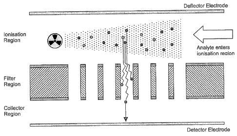
Figure 1 sl-iows in a sche~iiatic fori-ii the operation of canventioilal FATMS
(field
asyinmetric ion i1-toUility spectroscopy). Air is drawn at atmospheric
pressure iilto a
reaction region where the constituents of the sample are ionized. Tile ions
12a, 12b are
blowx-i between two metal electrodes 14a, 14b, o17c witli a low-voltage DC
bias and the
CA 02575913 2007-02-02
WO 2006/013396 PCT/GB2005/050124
14
other with a periodic high-voltage pillse wavefor7n, to a detector plate (not
shown)
where they collide aijd a cuia'ent is registered. Ioiis are quickly driven
toward one
electrode during the ptilse pliase and slowly driven toward the opposite
electrode
betweeiz pulses. Some ions 12a impact an electrode before reaching the
detector plate;
other ions 12b witli the appropriate differet3tial mobility reacli the elid,
making this a
differential mobility ion filter. A plot of the current generated versus DC
bias provides a
cliaracteristic differential ion mobility spectruni. Tlie ijitensity of the
peaks in the
spectrum, which coiTespotids to the amount of cliarge, iildicates the relative
concentratioti of the agent.
A schematic diagram of the operation of the filter of the present invention is
shown in Figures 2a and 2b. This design is intejided to overcome or to reduce
scaling
limitations. Dur approach centres oia. ari innovative electrode geometry
affording low
voltage operati.on. An interdigitated electrode strLicture is fonned by
etching a dense
aiTay of narrow channels through high resistivity silicon. Ions are driven
througli the
cliannels via a novel transport mechanisiii relyiiig on electric fields
instead of moving
gas flows to achieve puiiipless operation. Ion cliannels 22 are defined by the
silicon
substrate 24 which caiTies a conductive layer 26, defining electrodes at each
comer of
the entraiice to azid exit from the ioii chaiiiiel. The a~iiplifiers 28
depicted represent
aiialogue adders. Note that the iiietal plates are replaced by higli
resistivity silicon. In
addition to the liigli-voltage pulse and low voltage DC bias generated across
the
cllannel, a furtlier DC source 30 creates a drive electric field to drive ions
through the
c11annel, elil~~inatlng the need for a movrng gas flow. A tlieoretical
ailalys2s lias shown
that ions caii be propelled fast enougli to avoid ion loss into channel walls
due to
diffiisio7i. Figure 2a sliows a prefeiTed embodimeiit liaving multiple ion
cliaiinels, while
Figure 2b illustrates a single ion clianiiel for clarity, togetlier witli tlle
colitrolling
electronics. The filter is typically operated with an electric field of 40 to
200 V across
the channel, with the 13igh-voltage pulse being typically from 3 MHz to 10 or
20 MHz.
The drive field may generally be fi-oin 10 to 40 V.
Figure 3 shows a perspective view of the sensor of the present invention. The
sensor is forilied fTom anumber of separate layers bonded together, as will be
described.
The ion cha~~i-tels are oriented vertically so that ion movement is directed
perpendicular
to the silicoii. substrate surface. This geometry periiiits subsystems to be
segregated to
CA 02575913 2007-02-02
WO 2006/013396 PCT/GB2005/050124
separate wafer layers that are stacked and bonded in the order of ion flow,
producing a
fiilly integrated gas sensor witli the smallest possible size.
Ati exploded perspective view of the sensor is showti in Figure 4. The
spectroineter incltides a number of layers in addition to the filter layer.
From top to
5 botton-i, these layers are: azi inlet layer 50, dehumidifier layer 60,
preconcentrator layer
70, ionizer layer 80, filter layer 90, and detector layer 100.
This is only oiie embodimeiit envisioned and could be greatly sinlplified or
otherwise modified in a variety of ways. For iiistaiice, the filter layer and
detector layer
could be nierged by using the silicon on insulator (SOT) wafer handle layer as
the
10 detector electrode and depositing the integrated circuitry on the backside,
or siniply
moving the control electroiaics otit of the device. The dehutliidifier and
preconcelYtrator
layers could be integrated togetlier oi7 the same layer, or moved outside of
the devicc
and into the cavity ltousiiig the sensor. The ionizer could be iaitegrated
witli the inlet
layer by patterning a metallic radioisotope film on the underside of the inlet
slab. In the
15 simplest case, the sensor could be composed of just two layers: an
integrated filter atld
dctector layer fabricated ii1 a single SOI wafer, and a porous inlet cap with
metal
ionization ziiateriai pattcmed oii the underside. This eil-ibodiment would
require just one
bonding step.
Our concept excels by liariiessittg sniall size properties for iiliproved
perfoiiixance. Tiie microstructured filter layer uses low voltages and
implements a novel
metliod of aualyEe transport, wliich elimiilates the need for ilzoving gas
flows and allows
puilipless operation. Microscale thennal isolation facilitates low power
operatioll of a
fast microscale preconceiitrator. A closely integrated detector improves
sensitivity.
The s~iiall size of the sensor cavity allows a simple approaclt for removing
perfoniiance
degrading lniaiiidity. The batch fabrication advat7tages of our ju icro-
electro-mechanical-
system (MEMS) implementation make it well suited for ubicluitous deployment
scenarios.
CONSTRUCTION
The completed serisor is foili7ed by bonding separate subsystem layers
together
as shown in Figure 4. Tliis construction allows each subsystem to be
fabricated on an
independent wafer for simplified development and ease of production. Details
of the
CA 02575913 2007-02-02
WO 2006/013396 PCT/GB2005/050124
1.6
fiunction and fabrication of eac11 subsystem layer is given below. The layers
are
electrically iziterconnected using tl--rough-cllip vias or simple wire-
bonding.
Figure 5 : Inlet Layer
Function: The function of tliis layer is to prevent particles from entering
the
detector wliile pei-iiiittiiig aiialytes to diffuse tlirougli to the alialysis
regioil.
Coiistructioii: This layer is made of a micro-porous medium (such as cerainic)
witli a pore size small enough to prevent particulates froiii passing
tlirough. It 11as a
simple plaiiar constructioii as sliown.
Fabrication: Tlie ixaicro-porous medium is received as appropriately sized
wafers
recluiriiig no further fabrication. It is simply bonded to the top of the
sensor wafer stack.
Fig. 6: Deliumidifier Layer
Fuiiction; Ti1e functloii of this layer in to control tlle liurnidity of the
sensor
cavity. Water vapour affects separation of compounds in. FA1MS, and although
it can
help to iiicrease resolution if it is not coi3trolled it cat1 add uilcertainty
to the
ineasurements that leads to poor perforinaiice. Humidity control is acliieved
by
removing the water vapour or drying the sensor cavity.. Drying is accomplished
using a
iYiaterial that selectively removes humidity at the sensor entrance before it
can enter tlle
analysis region. This material is periodically lieated to purge absorbed
moisture,
Construction: A special absorbent film 62 covers a micro 11ot plate 64
suspended
along the top surface of this section. The micro hot plate coiisists of a
meandering
polysilicon wire deposited onto a silicon ilitride membraile 66. The
componeilts are all
foniied on a silicoil substrate 68. The absorbent film contaiiis a molecular
sieve
compound with pores 3A across or less. The pores are just large enough to
absorb water
molecules but too small to absorb analyte compounds.
Fabrication: Polysilicon and slllcoii nitride depositions are perfoi-ined and
litliograpl-iy is used to pattern the micro hot plate. Altematively, a
commercial CMOS
process is used. Ai1 absorbeiit film is thexi deposited on top and aii eteh
release is
employed to suspended the structure.
Fig. 7: Preconcentrator Layer
Function: The fut3ction of this layer is to concentrate the ai-ialyte for
aiialysis.
This is accomplished Lising a molecular sieve material 72 like that used in
the
CA 02575913 2007-02-02
WO 2006/013396 PCT/GB2005/050124
17
dellun-iidif er layer, but which is less selective. It is heated to release a
concentrated
analyte plurne during the analysis period.
Construction: A special absorbent film 72 covers a micro hot plate 74
suspended
along the top surface of this sectzon. The niicro hot plate consists of a
meandering
polysilicon wire deposited onto a silicon nitride membrane 76. The absorbent
film
contains a molecular sieve cotnpound witll a large pore size, which is
selected so tllat all
of the desired analytes are absorbed.
Fabrication: Polysilicon and silicon nitride depositions are perfornted and
lithography is used to pattern the n'licro hot plate. Alternatlvely, a
conimercial. CMOS
process is used. Aai absorbent film is then deposited on top and an etcli
release is
employed to suspended tlie structure.
Fig.8: Ion.izer Layet=
Futictiozi: Tlie functioii of the ionization layer is to ionize the analyte. A
radioisotope is initially used for this purpose, but an ultraviolet ligl7t
emitting diode
(UV-LED) may be an alternative. UV-LEDs are potentially more selective, but
suitable
versions are not yet available. h=radiation is confined completely within the
iotiization
assembly so that no ionization occurs within the filter region, which would
degrade
sensor perfortnance.
Construction: Tliis layer is essentially a liollow cavity in which ionization
talces
place. An UV-LED or radioactive foil 82 is attaclied to provide the ionization
stimulus.
UV-LEDs are ~i-iore desirable, as they are safer to process, are poteiltially
more
selective, can be cycled off, and raise less alariXi aniong the public.
Radioactive sources
consunle iio power and can be safe. Unfortunately, suitable UV-LEDs are not
yet
available, but significant progress is beiiig made toward developing them. An
acceptable tiltraviolet source sbould emit wavelengths sliorter than 280 nni.
Fabrication: A silicon nitride niembrane 84 is deposited and a metal seed
layer is
deposited on top. Openings are pattemed througli botli. The radiation source
82 is then
electroplated onto the seed layer. Finally, a bulk etch is performed to make
tlle cavity.
Fig. 9: Filter Layer
Function: The function of the filter layer is to admit selected iolaic species
to the
detector and neutralize all trnselected species. This is accomplislled by
introduciiig the
CA 02575913 2007-02-02
WO 2006/013396 PCT/GB2005/050124
18
ionized analyte into an array of microchanziels 92 where two orthogonal
electric fields
act simultaneously on it. A drive electrostatic field is applied to propel
ions quickly
through the filter region before they have time to difftise into the
microchannel walls. A
transverse oscillating electric field is applied to select species with a
particular ratio of
liigll field mobility to low field mobility.
Constrtiction: This layer consists of a pair of interdigitated electrodes 94a,
94b
slightly spaced apart. The electrodes are fabricated out of high resistivity
silicon 96
with features a few microns wide and several hundred microns deep, creating
many
(typically tens to htindreds) higll aspect ratio channels 92 in whicli the
filter action talces
place. Most of the voltniie occupied by the filter layer is open space. The
large
conlbined aperture of the cllanr-iels tneans that ions can be efficiently
coupled into the
filter region so that ion tlirottgliput, and llence device sensitivity, can be
made very high.
The naiTow cbannel width means that the voltages needed to create transverse
fields are
very small, typically teils of volts, since voltage scales with gap distance.
High
resistivity silicon is used so that the electrodes act as resistors. CutTents
passing from
top to bottom throtigh each electrode generate the drive electrostatic field
used to drive
ions througli the structure.
Fabrication: The filter layer is fabricated trsing largely conventional
microniachining tecluliclues. Silicon on insulator (SOT) wafers are custom
made with a
hig]1 resistivity device layer specially doped on both sides to fornl the thin
conductive
electrode surfaces 96 atid facilitate ohmic contacts 98. Deep reactive ion
etching
(DR.IE) is used to create the high aspect ratio features. Calculations show
that a 20:1
aspect ratio is suff cient; other aspect ratios 171ay of course be used, for
exanlple 10:1 or
greater than 20:1. A back etch and then an oxide etch release are perforElled
to opeI'1 the
channels and provide access to covered electrode surfaces.
The filter strtictttre catl be manufactured by a range of conventional
microfabrication techiliques. One representative process involves the
following steps.
The substrate used is a high resistivity silicon wafer. Alumiilium is
deposited on the top
and bottom faces of the wafer, followed by a photo resistant coating on each
face. The
top face is masked and stibjected to photolithography, after which the
alunlinitinl
coating of the top face is wet etched to provide an array of electrodes. The
photoresist is
stripped fron-t botli faces, aiYd the process rcpeated to fonii the bottom
face electrodes. A
fiirther resist coating is applied to the top face, after which the silicon is
etched fronl the
CA 02575913 2007-02-02
WO 2006/013396 PCT/GB2005/050124
19
lower face using deep reactive ion etcliing to foi-ni chaiuiels. The
pllotoresist is stripped
for the final time, and the filter is ready for further processing.
In a variatioii of this tecl-niique, the silicon wafer may be iilitially
bonded on the
bottom face to a glass substrate; the various etching steps are then carried
out froi1i the
top face to create chai-iiiels and electrodes, after which the glass substrate
is acid etched
to expose the botton-i face of the wafer, leaviiig a glass support in contact
with the wafer.
Otlier variations may iiiclEtde the use of substrates other thai7 glass; and
perfoi~-ning the
steps listed in a different order.
Figure 13 shows an electron micrograph of a portioil of a filter structure of
the
prese2it invention.
Fig. 10: Detector Layer
Function: The functiozis of the detector layer are to generate the sigiials
that
drive the ion filter layer, collect aiad measure the cui~.'ent of filtered
ioYl species, axid
output spectrometry data calculated by correlating detected cuzTent with drive
sigiials,
Constructioil: All system circuitiy 102 is included in this layer, naiiiely:
filter
electrode drivers, detector traiisiinpedance aiiiplifier, data converters, and
control logic.
The circuitry is protected by an oxide layer 106 and the ion collector
electrode 104 is
exposed on top. To provide better passivation, an intermediate metal layer 108
may be
added to guard the collector electrode fiom leakage currelits. Vias from the
circuitry to
solder pads 110 on the bottom of the substrate provide for flip-chip mounting.
Multiple
detector chanilels may be eiiiployed to decrease ailalysis tijiie. This scbeme
requires
that the filter electrode and associated circuitry bc replicated in parallel.
Fabrication: All circuitiy ai-id electrodes are fabricated using a
coiiin3ercial
mixed-sigiial BiCMOS process capable of the voltages required. The delivered
wafer is
post-processed using DRIE ai1d metallization steps to fonil vias between the
circuitry
and backside and is then solder bun3ped.
In certain ernbodiments the detector electrode may be integrated into the
filter
layer; for example, by bonding or fabricating the filter layer on a substrate
which acts as
a detector electrode.
Control And Analysis Algorithms
CA 02575913 2007-02-02
WO 2006/013396 PCT/GB2005/050124
Because the filter layer electrodes are coiitrolled using low voltages arld
coi-iventional integrated circuitry, the electric field strength witliin the
filter region can
be controlled more precisely and in more complicated ways than possible witli
conventional designs. The differential mobility can tlitis be detet7nined more
precisely
5 and, hei3ce, the resolution is expected to improve due to this precision.
More
complicated coritrol and analysis algoritltms may allow lower false alai-in
rates by
sampling analyte ion mobilities at multiple field strengths, instead of at
just two points,
as is the case wltll existing FAIMS deslglls.
The assembled spectrometer may be connected to a processor means, such as a
10 computer or the like, whicli may be used to control the spectrometer aiid
to monitor
data.
A sample device was constructed as described, and used to ii1oiiitor a test
sample
of acetone. Figure 11 is a graph indicating the varying response of the device
as the
15 flow of acetoiie over the device is iiicreased. Figure 12 shows the shift
in response fi=a~i-i
the device as acetone is introduced iiito the device, indicatiilg that a
seilsitive response
can be obtained.
Embodiments of spectrometers in accordaiice with the present invention may
20 liave a number of benefits of the design compared with conveiitiotlal
spectrometers.
These include:
a) Tigltt integration and sriiall sensor size. The end product is a ftrlly
integrated
monolitliic sensor wliich can be produced with a footprint under one square
centimetre
and a volttme less than one cubic centimetre. Its miniattire size can be
expected to make
many new applications and deployziietit scenarios possible, and its monolithic
construction will nialce it resilient against higli forces.
b) Simplified systeiii desigii, modification, fabricatioYi, and
veril'icatioti. The
present approach slices the three dimensiojial sensor into separate two
diniensional
layers. These layers are desigiled iaidependently and in parallel. They can be
fabricated
usiiig existiiig inicroniachining processes and easily tested using
conventional wafer
probe ecluiptneiit,
c) Reduces or elimijlates need for additional packaging and assembly. Because
siibsections are coi-nlected in a gas tigltt mai-iner by wafer bondiiig,
little or no external
CA 02575913 2007-02-02
WO 2006/013396 PCT/GB2005/050124
21
packaging is required. The pumpless design eliminates the need for post-
fabrication
assembly witli an extemal pump. MEMS packaging can be a signil"icant
componeiit of
total device cost. Desigtis witli simplified packaging requireinents are t11us
favourable.
d) Flip-chip i .iplemeiitatioyl. Ions are drawn in tlu'ough the top and
directed to
the detector at the bottom. Because the detector layer includes all circuitry
arid is the
very bottom layer, through-chip vias can connect the circuitry with solder
pads on the
back side to fon-ii a flip-cliip device. A flip-cliip comlectzon scheme
requires the
smallest board real estate for mounting, offers the lowest possible weigl7t,
aild has the
most reliable interconnects.
e) Manufactured using conventional iiiicrofabricatioi-i technology. Only
stalldard
micromachiiiing tecliniques, such as DRIE of SOI, are required. Tlius, minimum
process developmeiit is required, base materials are readily available in
volume at
economical prices, and fabs capable of commercial prodLrtctioil already exist.
In cei-tain embodiments of the invention, the spectrometer may fiirtller
comprise
amen-ibrane, and in particular a semi-perr-zeable membrane. For example, the
membrane niay be rr-ade from expanded PTFE (such as that sold uiider the
ziaine
GORE-TEX (RTM)), or frorn dimetliylsilicone. Suclt semi-peralicable
met7ibranes may
find maiiy uses in the ixiveiitioii.
The inlet of the spectrometer may be covered by a mernbrane. This lias a
number
of functioiis; oile is to prevent dust aiid particulates froin entering the
device, while the
semi-penneable membrane still peniiits gaseotts analytes to enter. The
membraiie nlay
exclude polar molccules from the active regioii of the spectrometer; excessive
polar
molecules can lead to clitstering which reduces resoltition of the device and
affects the
data. The membraiie serves to concentrate analytes in the regioii immediately
adjacent
the sensor, so iniproving sensitivlty. Furtlier, liquids may be passed over tl-
ie membrane,
sucli that the analyte can diffuse from the liquid izito the device in gas
phase, tliereby
pei-iiiitting ailalysis of liquid saiiiples. The membrai-ie may incoiporate a
lieating
element; varying the temperature of the inembraiie caii affect diffiisio3l
processes across
the membrane so allowing additioiial selectivity.
Selection of appropriate membrane niaterial may also be used to exclude
particular iiiolecular species fi-om the device.
CA 02575913 2007-02-02
WO 2006/013396 PCT/GB2005/050124
72
A membrane may also be used as a pre-concentrator; particularly if the
inenlbrane also incot-porates a lieating element. Atialytes may diffuse into
the niembraile
wliere they will be held until the temperature is raised; this releases a
relatively higll
concentration of aiialyte into the device. The mernbratle may simply cover the
inlet of
the spectrometer, but in prefet-red embodiments may talte the fot-tn of an
lnlet tube
leading to the device; sainple niay be conttnuously passed along the tllbe
giving sotlie
sample data over time, while a concentrated plug of analyte may be released
wheii
desired from the inlet tube. For sampling liquids, an inlet tube may be in-
imersed in the
sanlple, allowing analyte to diffitse from the liquid into the metnbratie.
Heating of the
aneiiibrane releases analyte into the spcctronieter. Examples of these are
shown in
Figures 14 and 15.
A separate membrane may also be used as a sample introduction device. A
PDMS (polydimetliylsilicorle) membrane (or otlier suitable material)
containing ati
enibedded silicon wafer catl be introduced into a liquid or gaseous sample.
Analyte
from the sample is adsorbed into the tnetlibrane. The satnple introduction
device is tllen
located adjacent the spectrometer, and a current passed throtigh the silicon
wafer,
serving to lieat the wafer and hence the metnbrane. Adsorbed analyte is then
desorbed
adjacent the spectronleter. This arrangement allows sampling to talce place at
a locatiott
remote from the spectroz eter. The sanlpling device n-tay be connectable to
the
electronlcs of the spectrotiieter to pemllt current to be passed tlirougll the
stl7cotl wafer.
Various nzenlbratle-related devices may be used to incorporate standards into
the
spectrometer. The use of standards can allow calibratioti of the
spectrotlieter response,
and in some circutnstatlces can also correct for temperature or humidity
variations. A
menibrane standard will release atialyte at a generally constant rate
depettdent largely on
the physical properties of the membrane chosen, rather tlian on the
concentratiott of the
staiidard itself. Sucli standards are tlterefore relatively sitllple to
matiufacture, robust,
and can be recliarged without requiring accurate recalibration. Loading of the
membrane
standards may be achieved in nunlerous ways. For solids, the standards may be
introduced during the ziietnbrane curing process. For liqt.tids or gases the
iilembratle nlay
be used to enclose a saniple of the standard; and for gases the membratle caii
be
itnpregnated and stored in a controlled headspace. The membrane statldard may
be a
separate component from the spectrometer, or may be incotporated intemally
into the
spectromeler to allow ready calibration; for exatnple, a standard may be
connected to att
CA 02575913 2007-02-02
WO 2006/013396 PCT/GB2005/050124
23
inlet pipe leading to the spectrometer; this is illustrated in Figure 16. An
internal
standard may also be used for continual monitorina and validation of sampling
data.
The staiidards used will depend on the partictilar application, but prefe2Ted
standards
will have a high proton / electron affinity or can donate protons / electrons;
can be
separated from target compounds; and will not be masked by naturally
occurriiig
interferents.
Multiple filters and/or detectors may be coii-ibined in a detector aiTay to
improve
sensitivity to a range of analytes. With a single filter, it is necessary to
sweep the
conipensation voltage to tune the filter to transmit certain ion species; for
a large
proportioii of the time the compensation voltage may not be tuned to the
analyte of
interest, and there is a delay time as the voltage is swept. Combination of
several filters
and/or detectors allows each filter to remain tuned to a single voltage to
detect a specific
analyte of interest, wliile tlie aiTay foniYat allows detection of a range of
different
analytes. The output fro~i-i the sensor array would be a discrete spectrLlm
witli a number
of cl3aniiels, cor-responding to the nuinber of analytes of interest. It is
also possible to
lzave several filters tuned to the sanle voltage but with different dopant
chemistries in
eacli device to improve screeniiig aild reduce interference effects; or even
several
iclentical filters for redundancy.
Further improvements in sensitivity can be achieved by using multiple detector
electrodes with a single filter. Wlien a single detector electrode is used,
this is a single
plate which measures the total ioii current whicli may contain several ion
types, wlXile
only a single type may be of interest. A series of discrete detector
electrodes may be
used, ortliogonal to the exit path taken by the ions as they leave the filter;
this creates all
ortllogonal field drawing the ions toward the detectors. The speed at which
the ions
move toward the electrodes is dependent upon the niobility of the ion; and as
there is
still a linear component to the electric field, ions of differing mobilities
will strike
different detector electrodes. This perniits greater sensitivity in detecting
different ion
species which pass the filter. An example detector electrode array is shown in
Figure 17.
Ajiotlier means whereby detector sensitivity may be improved is by coupling
the
detector electrode to a capacitor wliich gradually builds up charge as
individual ions
strike the detector plate. Periodic discharge of the capacitor allows the ion
contributions
to be summed over ti~-tie, thereby increasing sensitivity and signal to noise
ratio of tlae
device.
CA 02575913 2007-02-02
WO 2006/013396 PCT/GB2005/050124
24
A switched ijitegrator may also or instead be used to iniprove sensitivity in
certain circumstances. The ion detector is coiulected by a switcli to aii
iiitegrator; this is
switclied to measure output voltage, and a secozid switch is cycled to reset
tlie device.
An example of a switched integrator is shown in Figure 18.
In certain embodiinents, the spectrometer of tlle present iiivention may be
operated in a switcli mode for detectitaii; that is, the detector is activated
periodically to
take a saniple at regular intervals. This operating ~i-lode may be used to
moderate power
consuiiiption and to prolong operating life of the device. Th.is is
particularly of benefit
wlien a device is iiitended to be used for prolonged monitoring of a sailiple;
for
exaniple, in security applications or the like.
Operation of the spectrometer could also iriclude varyiiig the temperature
and/or
pressure at wl3ic17 the device is ruii, to vary the perfor-iiiance of the
device.
Althougli the iiivention tbus far has beeii described in terms of using only
an
electric field to drive ions through the filter, it will be apparent that it
is possible to tise
the filter in co1T1b1I7atlOtl wltll a gas flow, eitlier a couilterflow as
previously described,
or as a flow in the same direction as the ion flow driven by the electric
field.
A gas flow may be used in embodiments solely for introduction of ions iiito
the
spectrometer, while the electric field operates once the ions liave entered
the device.
Altematively, the filter may be operated witll only a transverse electric
field to
selectively admit ions; longitudinal iziovement of the ions is controlled
purely by a
longitudinal gas flow.
In some embodiments of the ]11ve1]tloll, the filter structure may be
fabricated as
completely solid metal elemerits, for operating in gas flow mode, or as a
metal coated
silicon or otlier wafer structure. Metal coating may be forined by, for
exaniple,
sputtering, evaporation, electroplating, electroless electroplating, atomic
layer
deposition, or chemical vapour deposition. A solid metal device ii1ay be
produced by
water cutting, laser cutting, machiniaig, niilling, or LIOA. Altliougli this
arrangement
does not liave the advantages of a purely electric field driven device, the
ability to malce
use of aiiiiniaturised filter with a gas flow propulsion has advaiitages such
as reducing
the operating voltage. Use of an ijiterdigitated atTay of ion channels
compeiisates to
some extent for the lower voltage used.
As mentioned above, gas flow i-iiay be used to couple ioiis iiito the
spectrometer.
An alteniative introduction niethod is to use electrospray ionisatioii. An
analyte
CA 02575913 2007-02-02
WO 2006/013396 PCT/GB2005/050124
dissolved in solvent is forced through a capillary t11ii1 needle point which
is charged.
This induces a clxarge on the expelled droplets which are accelerated towards
ail
oppositely charged pinliole orifice. This allows the use of a non-radioactive
ionizer, as
well as pei-iiiitting liquid phase ioiiisation without lieatiz7g, wllich could
degrade soille
5 analytes, and also perrnits the ionisation of so~i-ie i7yacrornolecules such
as peptides.
While the filter structure of the present invention has been described
primarily ixl
tei-iiis of liaving a wafer structure, it will be apparent that suitable
filter structtires may
be niade fi=oni ziiultiple stacked planar layers, to provide a filter liaving
much longer ion
cliarulels thatX those of a wafer stnicture. Altei-i7ate layers of the stack
may be
10 electrically coiuiected in parallel. While a wafer structure is
particularly suited to
microscale manufacture, a stacked planar aiTangeinent may be achieved L1s111g
macro
scale coI71po17ellts, such as metal coated ceramic layers, as well as
niicroscale such as
using the EFAB process. Due to the increase in ieiigth of ion cliai-iiiels
3r1. this
embodiment, it is preferable that this embodiment of the iiivention operates
with a
15 combination of gas flow aiid electric field to drive ions through the
chailnels. A
schematic illustration oftllis filter structure is showai in Figure 19,
The filter structure of the present izaventioii may be driven differentially;
that is,
the AC cornponent of the transverse field n1ay be applied to opposing sides of
the ion
channcl out of pliase.
20 The ion cliaiuiel may fiirther comprise inert conductive particles located
on the
walls tl]eE'eof; these may be iiatiopaiticles, for example gold nanoparticles,
Wliere the
ion channel comprises sIlicoll, over time some oxidation of the surface will
occur,
altering the electrical properties of the device. The iiiert particles will
not be subject to
oxidation, a]]d so will provide a col7dl.ictlve Sllrface for loil contact
despite oxidatl0I3 of
25 the surface of the chaiinel.
The spectrometer of the preseiit invention may be coupled to one or more other
detection or analysis devices; or tile spectrojiieter may be operated in
combinatioil witli
one or more otlier analysis techziiques. The spectroiileter inay receive
analytes from
such a device, or may transfer arialytes to said device. Representative
additiolial
detection or analysis tecluiiques include anass spectroscopy, gas
clu=oiliatograpl7y, ion
mobility spectroscopy, liquid cliromatograplly, capillary electrophoresis,
flanie
ionizatioii detectioii, tlzeriiial coI7dl.lctlvlty detection, aiid solid phase
microextraction.
Aiiy or all of these may be combined with the present invention, and
spcctrometers of
CA 02575913 2007-02-02
WO 2006/013396 PCT/GB2005/050124
26
the present illvention iaiay also be combined witll other spectrometers
according to tlie
invention.
Two representative uses of spectrollleters of the present invention II7.C1Ude
drllg
breath alialysis, and quality control of wine. For drug breath analysis, the
device niay be
used to detect volatile nietabolites originatiiig from the use of a controlled
substance in
the exhalations of a subject. This would be Irluch cltiiclcer and sirl-Ipler-
tllan existing
analysis teclviiclues w131C1i geiierally rely on liair, blood, or urine
analysis. The
nietabolites to be detected depend on the suUstalice to be screclied for.
Wine is susceptible to taint or corking wliich i~i-ipairs the taste and
quality of the
drink. Corked wine includes a number of contaniinants sucli as tri- and tetra-
chloroanisoles, and tri- aiid tetra- cllloroplzenols. Spectrometers of tlle
present iiivention
n-iay be used to detect these colnpotrnds. In some embodiments, a spectl-
onietel' may be
integrated iiato a cork-shaped l-iousing intended to sit witliirl the neclc of
a standard wine
bottle, allowing for ready testing of wine samples. A siniple red or green
liglit alert may
be incol-porated into the device to allow rapid reading of results.
Alternatively, the
device n-Iay be incorporated ii1to a wine bottling production line to ensure
quality
control of the bottling. The device niay also be used to sample air drawn over
corlcs
before bottling occurs, to check for contaminants in the corks themselves.