Note: Descriptions are shown in the official language in which they were submitted.
CA 02575990 2007-02-02
WO 2006/017393 PCT/US2005/027012
EMBEDDED CONTROL VALVE USING HOMOPOLAR MOTOR
BACKGROUND OF THE INVENTION
Description of the Related Art
Miniaturization of various devices which incorporate
fluidic systems has spurred a need for fluidic systems having
very small components. These systems are commonly known as
microfluidic systems. Microfluidic systems have the potential
to play an increasingly important role in many developing
technology areas. For example, there has been an increasing
interest in recent years in the use of liquid fuels in
microengines and in the use of fluid dielectrics in
electronics systems.
Another technological field where micro-fluidic
systems are likely to play an increasingly important role is
fuel cells. Fuel cells generate electricity and heat by
electrochemically combining a fuel and an oxidant, via an ion-
conducting electrolyte. Some types of fuel cells produce
waste water as a byproduct of the reaction. This waste water
must be transported away from the reaction to be exhausted
from the system by a fluid management sub-system.
Efforts are currently under way to create very small
fuel cells, called microcells. It is anticipated that such
microcells may eventually be adapted for use in many portable
electronics applications. For example, such devices could be
used for powering laptop computers and cell phones. Still,
microcells present a number of design challenges that will
need to be overcome before these devices can be practically
implemented. For example, miniaturized electro-mechanical
systems must be developed for controlling the fuel cell
reaction, delivering fuel to the reactive components and
disposing of water produced in the reaction. In this regard,
innovations in fuel cell designs are beginning to look to
-1-
CA 02575990 2007-02-02
WO 2006/017393 PCT/US2005/027012
silicon processing and other techniques from the fields of
microelectronics and micro-systems engineering.
As with most other types of fluidic systems,
microfluidic systems usually incorporate control valve devices
that are implemented as discrete components. Discrete
components tend to be bulky, however, which oftentimes impedes
miniaturization efforts. Moreover, such control valve devices
typically include pluralities of moving parts that must
interoperate. The reliability of such devices, however, is
generally inversely proportional to the number of moving parts
since the moving parts tend to wear. Hence, an embedded
control valve that can overcome the aforementioned limitations
is needed for use in microfluidic systems.
SUbII4ARY OF THE INVENTION
The present invention relates to a method for
controlling fluid flow. A fluid can be communicated to a
first fluid flow port disposed adjacent to a first surface of
a rotatable disk of a homopolar motor. The fluid can flow
through at least one orifice in the rotatable disk to a second
fluid flow port. The rotation of the disk can be selectively
controlled to vary a fluid flow rate. Further, the disk can
be rotated to align a selected one of the orifices with at
least one of the first and second fluid flow ports. In
another arrangement, the shape of the orifice can have a
radial width that increases in a circumferential direction.
The disk can be resiliently biased toward a first
rotation position. Further the disk can be rotated by flowing
an electric current through the disk in the presence of a
magnetic field aligned with an axis of rotation of the disk.
The invention further includes a fluid flow valve
with a homopolar motor having a rotatable disk with at least
one orifice. The orifice ca:z have a radial width that
increases in a circumferential direction. A first fluid flow
-2-
CA 02575990 2007-02-02
WO 2006/017393 PCT/US2005/027012
port can be disposed adjacent to a first surface of the disk
and a second fluid flow port can be disposed adjacent to a
second surface of the disk.
The disk can be rotationally operable between a
first position and at least a second position such that fluid
flows from the first fluid flow port through the orifice in
the first position, and the flow of fluid is reduced in the
second position. The disk can be continuously variable
between the first position and the second position. The
microfluidic control valve can include a closed loop control
circuit and at least one sensor to control the amount of
rotation of the disk. The sensor can be an optical sensor, a
hall sensor, a fluid flow sensor or an electrical current
sensor. A biasing member can be included which resiliently
biases the rotatable disk.
The disk can be disposed within a cavity defined in
a substrate. The substrate can be a ceramic substrate, a
liquid crystal polymer substrate or a semiconductor substrate.
A fluid channel fluidically coupled to the first fluid flow
port also can be defined within the substrate.
BRIEF DESCRIPTION OF THE DRAWINGS
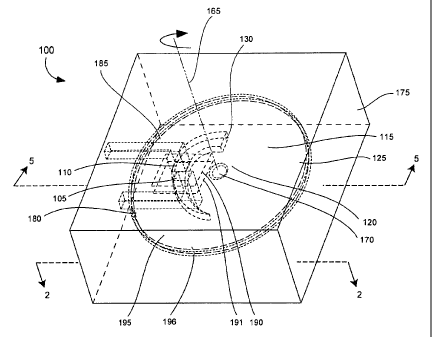
Fig. 1 is a perspective view of a microfluidic
control valve that is useful for understanding the present
invention.
Fig. 2 is section view of a microfluidic control
valve of Fig. 1, taken along section line 2-2.
Fig. 3 is a section view of an alternate embodiment
of the microfluidic control valve.
Fig. 4 is a section view of another embodiment of
the microfluidic control valve.
Fig. 5 is a cross section of the microfluidic
control valve of Fig. 1 taken along section line 5-5.
-3-
CA 02575990 2007-02-02
WO 2006/017393 PCT/US2005/027012
Figs. 6A-6C illustrate a process for manufacturing
the microfluidic control valve on a dielectric substrate,
which is useful for understanding the present invention.
Figs. 7A-7H illustrate a process for manufacturing
the microfluidic control valve on a semiconductor substrate,
which is useful for understanding the present invention.
Fig. 8 is a schematic diagram of a fluidic system
that is useful for understanding the present invention.
Fig. 9 is a flow chart that is useful for
understanding the present invention.
DETAILED DESCRIPTION OF THE PREFERRED EMBODIMENTS
The present invention relates to a microfluidic
control valve (control valve). The control valve can be used
in microfluidic systems to control a fluid flow rate, as well
as to turn on and turn off fluid flow. Importantly, the
control valve can be embedded in a substrate containing a
fluid flow channel through which the fluid flows. The control
valve can include a microelectromechanical homopolar motor
(homopolar motor) to impede fluid flow as required via
rotation of a disk having at least one orifice through which
the fluid can flow. Through the rotation of the disk, the
alignment of the orifice with respect to a fluid flow port can
be varied, and thus provide a variable fluidic impedance.
Notably, the disk can be very small. For example, the disk
can have a diameter that is smaller than 1 cm, or even smaller
than 1 mm. Accordingly, the system profile of the
microfluidic system is smaller in comparison to fluidic
systems using discrete components. Additionally, there are a
reduced number of fluidic seals in the microfluidic system,
thereby making the microfluidic system comparatively more
robust.
The control valve can be a stand alone device or can
be advantageously integrated with a larger system on the
-4-
CA 02575990 2007-02-02
WO 2006/017393 PCT/US2005/027012
substrate. Examples of such larger systems can include fuel
cells, micro-motors, and other MEMS type devices. Other
examples can include fluid dielectric based devices in the RF
field such as antenna elements, matching sections, delay
lines, beam steering elements, tunable transmission lines,
stubs and filters, variable attenuators, and cavity
structures. Still, the invention is not limited to any
particular type of device.
A control valve 100 in accordance with the present
invention is shown in Fig. 1. The control valve 100 can be
manufactured on a variety of substrates. For example, the
control valve 100 can be manufactured on a substrate made of
liquid crystal polymer (LCP), ceramic, silicon, gallium
arsenide, gallium nitride, germanium or indium phosphide.
Still, the invention is not so limited and any substrate
material suitable for a micro-electromechanical manufacturing
process can be used.
The control valve 100 can include a first fluid flow
port 105 and a second fluid flow port 110. The control valve
100 also includes a rotatable conductive disk (disk) 115, or
rotor, having a central portion 120 and radial edge portion
125. At least one orifice 130 can be provided in the disk
115, located between the central portion 120 and the radial
edge portion 125 of the disk. As defined herein, an orifice
is an opening in the disk 115 through which fluid may flow.
Although an orifice may have a continuous perimeter defined
between the central portion 120 and the radial edge portion
125, as used herein the term is not so limited. For instance,
an orifice within the meaning of this specification also may
be only partially bounded by the material forming the disk
115. When fluid flow is desired, the orifice can be aligned,
or partially aligned, with at least one of the fluid flow
ports 110, 115.
-5-
CA 02575990 2007-02-02
WO 2006/017393 PCT/US2005/027012
Referring to Fig. 2, a section view of the control
valve taken along section line 2-2 is shown. The orifice 130
of the disk 115 can be defined by a continuous perimeter 235
of an opening 240 within the diFk 115. For example, the
orifice 130 can be elongate having a first end 245 and a
second end 250. The second end 250 can be narrower than the
first end 245. Moreover, a width 255 of the orifice can
decrease from the first end 245 to the second end 250. n
this arrangement, fluid flow adjustment can be continuously
varied by rotating the disk 115 to adjust alignment of the
orifice 130 with one or both fluid flow ports. For instance,
if a small amount of fluid flow is desired, the disk 115 can
be oriented so that the second (narrower) end 250 of the
orifice 130 is aligned with the fluid flow port 105. If a
greater amount of fluid flow is desired, the disk 115 can be
oriented so that the first (larger) end 245 of the orifice 130
can be aligned with one or both of the fluid flow ports 105,
110. Moreover, if it is desired that there be no fluid flow,
a portion 260 of the disk 115 not having an orifice can be
aligned with the fluid flow port 105.
In another arrangement of the control valve 100, as
shown in Fig. 3, an orifice 305 can be defined by a radial
discontinuity in a perimeter 310 of the disk 115 (i.e. the
perimeter 310 of the disk 115 does not have a constant radius
315 from the central axis 165 of the disk 115). For example,
at a first end 320 of the orifice 305 the disk 115 can have a
smaller radius 315 as compared to a second end 325 of the
orifice 305.
In a first position, the disk 115 can be disposed
such that the first end 320 of the orifice 305 is near the
fluid flow port 105 such that the fluid flow port 105 is
unimpeded by the disk 115. The disk can be rotated to a
second position such that the second end 325 of the orifice
305 is near the fluid flow port 105 and flow of fluid through
-6-
CA 02575990 2007-02-02
WO 2006/017393 PCT/US2005/027012
the fluid flow port 105 is impeded by the disk 115. As the
disk 115 is rotated between the first and second positions,
the perimeter 320 of the disk 115 can extend over the fluid
flow port 105 and change the fluidic impedance at the port.
In a position where a portion 330 of the disk 115 having a
maximum radius 315 is proximate to the fluid flow port 105,
the flow of fluid through the fluid flow port 105 can be
stopped. For example, in the present example, the disk 115
can be rotated clockwise so that the fluid flow can be
gradually reduced until fluid flow is stopped. The fluid flow
can be stopped more abruptly by rotating the disk 115 counter
clockwise so that the end 320 of the orifice passes over the
fluid flow port 105 to place the portion 330 of the disk
between the fluid flow ports 105.
In yet another embodiment of the control valve 100,
multiple orifices 430 can be provided, as shown in Fig. 4. In
this arrangement, fluid flow can be adjusted in discrete
steps, as opposed to the fluid flow being continuously
variable. For example, the disk 115 can be rotated until an
orifice 430 having an appropriate size for the desired fluid
flow is positioned over the fluid flow port 105.
At this point it should be noted that the
embodiments disclosed in Fig's. 2-4 are presented for
exemplary purposes only, and the present invention is not
limited to the precise disk and orifice embodiments presented
herein. For instance, while keeping in accordance with the
present invention, disks and/or orifices can be provided to
have any shapes or configurations that are suitable for
controlling fluid flow through the control valve using one or
more homopolar devices.
Referring again to Fig. 1, the disk 115 can be
positioned proximate to a substrate surface, for example
within a cavity 180 defined within a substrate 175.
Importantly, the cavity 180 can have a shape that is
-7-
CA 02575990 2007-02-02
WO 2006/017393 PCT/US2005/027012
substantially circular, square, rectangular, or any other
desired shape. In one arrangement, the disk 115 can be
provided with an axle 170 to facilitate rotation about the
central axis 165 of the disk 115 and maintain the disk 115 in
the proper operating position. Nevertheless, other
arrangements can be provided as well. For example, in another
arrangement the cavity 180 can be structured with a low
friction peripheral surface 185 that maintains the disk 115
within the cavity 180. In yet another arrangement, a hole can
be provided at the central axis 165 of the disk 115. The hole
can fit over a cylindrical structure, such as a bearing, to
maintain the operating position of the disk 115.
Gaskets 190, 191 can be provided to form a seal
between the disk 115 and the first and second ports 105, 110,
thereby directing fluid through the orifice 130. For example,
a gasket 190 can be provided between an upper surface 195 of
the disk 115 and the second fluid flow port 110, and a gasket
191 can be provided between lower surface 196 of the disk and
the first fluid flow port 105. In the case that the fluid
which flows through the control valve 100 is a dielectric,
seepage of fluid beyond the seal into cavity 180 typically
will not present a problem so long as the dielectric is not
corrosive to the disk 115 or the other components that may be
contained in the cavity 180. However, in the case that the
fluid is conductive, it can be beneficial to provide multiple
gaskets both above and below the disk 115 to minimize the risk
of fluid seepage into the cavity 180.
Referring to Fig. 5, a cross section is shown of the
control valve 100 of Fig. 1 taken along section line 5-5. The
rotatable disk 115 is immersed in a magnetic field,
illustrated with magnetic field lines 505, which are typically
perpendicular to a surface 510 of the disk 115. One or more
magnets 530 can be provided above and/or below the disk 115 to
-8-
CA 02575990 2007-02-02
WO 2006/017393 PCT/US2005/027012
generate the magnetic field. The magnets 530 can include
permanent magnets and/or electromagnets.
A first contact brush 515 can contact the disk 115
near its central portion 120, which is proximate to the disk
central axis 165. A second contact brush 520, which can be
radially spaced from the first contact brush 515 to contact
the radial edge portion 125 of the disk 115. The second
contact brush 520 can extend over a portion of the radial edge
125, or circumferentially extend under or around the entire
radial edge 125.
In one arrangement, a contact brush (not shown) can
be provided to contact the axle 160. Additional contact
brushes also can be provided. For example, contact brushes
can be spaced in a circular pattern to contact multiple points
on the radial edge 125. Similarly, contact brushes can be
spaced near the central portion 120 of the disk 115 to contact
the central portion 120 at multiple points, to form a
continuous circumferential contact surface at the central
portion 120, or to contact the axle 160.
When voltage is applied across the contact brushes
515 and 520, causing current to flow through the disk 115,
magnetic forces are exerted on the moving charges. The moving
charges in turn exert the force to the disk 115, thereby
causing the disk 115 to rotate. Notably, the direction of
rotation depends on the direction of the current flow through
the disk 115, for example, whether the current flows from the
central portion 120 of the disk 115 to the radial edge portion
125, and vice versa. Accordingly, the polarity of the applied
voltage can be changed when it is desired to change the
direction of rotation of the coriducive disk 115.
In one arrangement control stops can be provided to
limit the amount of rotation of the disk 115. For example, a
raised nub 535 can be disposed on the disk 115 at a radial
distance from the central axis 165 of the disk 115. A
-9-
CA 02575990 2007-02-02
WO 2006/017393 PCT/US2005/027012
plurality of raised nubs 540 can extend downward from an upper
portion 545 of the substrate 175. The raised nubs 540 can be
positioned at an approximately equivalent radial distance from
the central axis 165 as the raised nub 535 at
circumferentially offset locations. The raised nubs 535, 540
can be disposed on their respective surfaces such that the
raised nub 535 abuts against a first one of the raised nubs
540 in a position of maximum clockwise rotation of the disk
115, and the raised nub 535 abuts a second one of the raised
nubs 540 in a position of maximum counterclockwise rotation.
Still, there are a number of other methods that can be used to
limit the rotation of the disk 115 and the invention is not so
limited.
In one arrangement the disk 115 can be resiliently
biased into a particular position. For example, the disk 115
can be biased into a maximum clockwise rotation, a maximum
counter clockwise rotation, or any other desired amount of
rotation. To bias the disk 115, one or more biasing members
565 can connect between the disk 115 or axle 160 and any other
non-rotational structure within the control valve 100. For
example, the biasing members 565 can be springs, elastic
members, or any other device that can be used to bias the disk
115. In this arrangement, an amount of electric current
conducted through the disk and/or a strength of the magnetic
field can be controlled to achieve a desired amount of disk
115 rotation.
In another arrangement, an electric current (bias
current) can be conducted through the disk 115 to bias the
disk 115. For example, a small amount of current can flow
through the disk 115 to maintain the disk 115 in a maximum
clockwise or counter clockwise rotation. The bias current can
be removed when rotation of the disk 115 is desired.
As noted, gaskets 190, 191 can be provided to form a
seal between the disk 115 and the first and second ports 105,
-10-
CA 02575990 2007-02-02
WO 2006/017393 PCT/US2005/027012
110, thereby directing fluid through the orifice 130.
Further, a sensor 550 can be provided for monitoring the
amount of disk rotation. For instance, the sensor 550 can be
included in a closed loop control system which controls the
rate of fluid flow. Such control systems are known to the
skilled artisan. For example, the sensor can be an optical
sensor which reads marks on the disk 115 that represent an
amount of disk rotation. The marks can correlate to a width
of a portion of the orifice 130 which is currently disposed
between the fluid flow ports 105, 110. In another
arrangement, an optical sensor also can be used to measure a
width of the orifice 130 in the disk 115.
The sensor 550 also can be a Hall sensor that is
used to measure the width of a portion of the orifice 130
which is currently disposed between the ports 105, 110. In
particular, a portion of the disk 115 having a wider portion
of the orifice 130 will have less material than a portion of
the disk 115 having a narrower portion of the orifice 130.
The Hall sensor can be used to measure changes in magnetic
influence due to changes in the amount of material in
respective portions of the disk 115.
In yet another arrangement, the sensor 550 can be a
fluid flow sensor located proximate to a fluid channel 555 to
measure the flow of fluid 560 within the channel 555. The
sensor 550 also can be an electrical current sensor that
monitors the electrical current through the disk 115, from
which the amount of disk rotation can be determined. Still,
there are a myriad of other sensors known to the skilled
artisan that can be used to control the operation of the
control valve, and thus the invention is not limited to the
examples discussed herein.
Figs. 6A-6C represent one manufacturing process that
can be used for manufacturing the control valve on a ceramic
substrate. Nevertheless, it should be noted that the
-11-
CA 02575990 2007-02-02
WO 2006/017393 PCT/US2005/027012
structures represented in Figs. 6A-6C also can be implemented
for manufacturing the control valve with other types of
substrates, for example with LCP substrates. It should be
noted, however, that the lamination and curing processes can
differ for each type of substrate, as would be known to the
skilled artisan.
One LCP substrate that can be used is R/flex 3000
Series LCP Circuit Material available from Rogers Corporation
of Rogers, CT. The R/flex 3000 LCP has a low loss tangent and
low moisture absorption, and maintains stable electrical,
mechanical and dimensional properties. The R/flex 3000 LCP is
available in a standard thickness of 50 pm, but can be
provided in other thicknesses as well.
One ceramic substrate that can be used is low
temperature 951 co-fire Green TapeTM from Dupont . The 951 co-
fire Green TapeTM is Au and Ag compatible, and has acceptable
mechanical properties with regard to thermal coefficient of
expansion (TCE) and relative strength. It is available in
thicknesses ranging from 114 pm to 254 pm. Other similar
types of systems include a material known as CT2000 from W. C.
Heraeus GmbH, and A6S type LTCC from Ferro Electronic
Materials of Vista, CA. Any of these materials, as well as a
variety of other LTCC materials with varying electrical
properties can be used.
Referring to Fig. 6A, a first substrate layer 602
can be provided. The substrate material that is to be used in
each of the substrate layers can be preconditioned before
being used in a fabrication process. For example, if the
substrate is ceramic, the ceramic material can be baked at an
appropriate temperature for a specified period of time or left
to stand in a nitrogen dry box for a specified period of time.
Common preconditioning cycles are 160 C for 20-30 minutes or
24 hours in a nitrogen dry box. Both preconditioning process
are well known in the art of ceramic substrates.
-12-
CA 02575990 2007-02-02
WO 2006/017393 PCT/US2005/027012
Once the first substrate layer 602 is
preconditioned, a fluid channel 630 can be formed in the first
substrate layer 602 for carrying fluid through the control
valve. In the arrangement shown, the fluid channel 630
extends from a bottom surface 632 of the first substrate layer
602 to a top surface 634 of the substrate layer 602, but the
invention is not so limited. For instance, in the case that a
substrate layer is used that is thicker than the desired
diameter of the fluid channel 630, the fluid channel 630 can
be contained between the bottom surface 632 and the top
surface 634, and a via can be used to tap into the fluid
channel 630 where desired.
A conductive via 636 can be formed in the first
substrate layer 602 to provide electrical conductivity through
the substrate layer. Many techniques are available for
forming conductive vias in a substrate. For example, vias can
be formed by mechanically punching holes or laser cutting
holes into the substrate. The holes then can be filled with a
conductive material, such as a conventional thick film screen
printer or extrusion via filler. Vacuum can be applied to the
first substrate layer 602 through a porous stone to aid via
filling. Once the conductive via 636 has been formed in the
first substrate layer 602, the conductive material can be
dried in a box oven at an appropriate temperature and for an
appropriate amount of time. For example, a common drying
process is to bake the ceramic substrate having the conductive
material at 160 C for 5 minutes.
After the conductive filler in the via has dried, a
first conductive circuit trace 638 and a second conductive
circuit trace 640 can be provided. The circuit traces 638,
640 can be deposited onto the first substrate layer 602 using
a conventional thick film screen printer, for example,
standard emulsion thick film screens. In one arrangement, the
circuit traces 638, 640 can be deposited onto opposite sides
-13-
CA 02575990 2007-02-02
WO 2006/017393 PCT/US2005/027012
of the first substrate layer 602, with the first circuit trace
638 being in electrical contact with the conductive via 636.
The second circuit trace 640 can extend around, and be
concentric with, the conductive via 636. Nonetheless, a
myriad of other circuit layouts can be provided, as would be
known to the skilled artisan. As with the via filling
process, once the circuit traces have been applied to the
first substrate layer 602, the circuit traces can be dried in
a box oven at an appropriate temperature and for an
appropriate amount of time.
Subsequent substrate layers can be laminated to the
first substrate layer 602 after appropriate preconditioning
and drying of the circuit traces and/or via fillers. In
particular, a second substrate layer 604 can be stacked onto
the first substrate layer 602. The second layer 604 can
insulate circuit traces on the top of the first substrate
layer 602. The second substrate layer also can include vias
642, 644, which can be filled with material to form an axial
contact brush 646 and at least one radial contact brush 648,
respectively. The vias can be positioned so that the contact
brushes are electrically continuous with respective circuit
traces 638, 640. In one arrangement, a plurality of radial
contact brushes 648 or a continuous radial edge contact brush
can be disposed concentric with, and at a uniform radius from,
the axial contact brush 646 to reduce a net contact resistance
between the a conductive object and the brushes.
The contact brushes can include any conductive
material suitable for use in a contact brush, for example a
conductive epoxy, conductive polymer, carbon nano composite or
a conductive liquid. In the case that the contact brushes are
a solid material, such as carbon nano composite, the contact
brushes can be screen printed into the vias in the second
substrate layer 604 using a conventional thick film screen
printer. In the case that a conductive liquid is used as
-14-
CA 02575990 2007-02-02
WO 2006/017393 PCT/US2005/027012
contact brushes, ferromagnetic properties can be incorporated
into the conductive liquid so that a magnetic field can
contain the conductive liquid within the vias 642, 644. In
one arrangement, the axial contact brush 646 can fill only
part of the via 642 so that a top surface of the via is
disposed below an upper surface 654 of the second substrate
layer 604. Accordingly, the via 642 also can function as a
bearing. The second substrate layer 604 also can include a
fluid channel 650 extending from a lower surface 652 to the
upper surface 654 of the second substrate layer 604. The
fluid channel 650 can align with a portion of the fluid
channel 630 so that fluid can flow between the fluid channels
630, 650.
A third substrate layer 606 can be stacked above the
second substrate layer 604. The third substrate layer 606 can
incorporate an aperture 656 having a radius edge 658 aligned
with an outer radius of vias 644 (a portion of each via
furthest from the via 642). A fourth substrate layer 608 can
be stacked below the first substrate layer 602 to insulate
circuit traces on the lower surface 632 of the first substrate
layer 602. Further, a fifth substrate layer 610 can be
stacked below the fourth substrate layer 608. The fifth
substrate layer 610 also can include an aperture 660 having an
outer radius 662.
A sixth substrate layer 614 can include a fluid
channel 664 extending from a lower surface 666 of the sixth
substrate layer 614 to an upper surface 668 of the sixth
substrate layer 614. Further, a seventh substrate layer 616
can include a fluid channel 670 extending from a lower surface
672 to the upper surface 674 of the seventh substrate layer
616. The fluid channel 670 can align with a portion of the
fluid channel 664 so that fluid can flow between the fluid
channels 664, 670. Finally, an eighth substrate layer 618 can
be provided.
-15-
CA 02575990 2007-02-02
WO 2006/017393 PCT/US2005/027012
In some instances it can also be desirable to
include a conductive ground plane (not shown) on at least one
side of one or more of the substrate layers 602, 604, 606,
608, 610, 614, 616, 618. For example, the ground plane can be
used in those instances where RF circuitry is formed on the
surface of a substrate layer. The conductive ground plane
also can be used for shielding components from exposure to RF
and for a wide variety of other purposes. The conductive
metal ground plane can be formed of a conductive metal that is
compatible with the substrate. Still, those skilled in the
art will appreciate that the ground plane is not required for
the purposes of the invention.
Referring to Fig. 6B, the first five layers 602,
604, 606, 608, 610 can be stacked to form a bottom substrate
structure 686 and define a fluid channel 690. The substrate
layers 614, 616, 618 can be stacked to form a top substrate
structure 688 and define a fluid channel 692. Importantly, it
should be noted that the layer scheme presented herein is by
example only. A greater number or a fewer number of substrate
layers also can be used.
Once the substrate layers have been stacked to form
the substrate structures 686, 688, each of the structures 686,
688 can be laminated using a variety of lamination methods.
In one method, the substrate layers can be stacked and
hydraulically pressed with heated platens. For example, a
uniaxial lamination method presses the substrate layers
together at 3000 psi for 10 minutes using plates heated to 70
C. The substrate layers can be rotated 165 following the
first 5 minutes. In an isotatic lamination process, the
substrate layers are vacuum sealed in a plastic bag and then
pressed using heated water. The time, temperature and
pressure can be the same as those used in the uniaxial
lamination process; however, rotation after 5 minutes is not
-16-
CA 02575990 2007-02-02
WO 2006/017393 PCT/US2005/027012
required. Once laminated, the structures 686, 688 can be
fired inside a kiln on a flat tile. For example, the
substrate layers can be baked between 200 C and 500 C for one
hour and a peak temperature between 850 and 875 can be
applied for greater than 15 minutes. After the firing
process, post fire operations can be performed on the
substrate layers.
Referring to Fig. 6C, the disk 115 can be provided
within the cavity 180. The disk 115 can be comprise a
conductive material, such as aluminum, copper, brass, silver,
gold, steel, stainless steel, or any other rigid conductive
material. In another arrangement, the disk 115 can comprise a
plurality of materials, for example a semi-rigid conductive
material that is laminated to a rigid material, for instance
ceramic. The disk 115 can include a central contact 676
axially located on the lower surface 196, and at least one
radial contact 678, also located on the lower surface 196. In
one arrangement, the radial contact 678 can extend around the
lower peripheral region 680 of the disk 115. The disk 115 can
be positioned above the second substrate layer 604 so that the
central contact 676 makes electrical contact with the axial
contact brush 646 and the radial contact 678 makes electrical
contact with the radial edge contact brush 648. Accordingly,
electrical current can flow between central portion 120 and
radial edge portion 125 when voltage is applied across the
contact brushes 646, 648. The radial wall 682 of the via 642
can function as a bearing surface for the central contact 676
of the disk 115. Alternatively, bearings (not shown) can be
installed between the radial wall 682 and the central contact
676. The bearings can be, for example, electromagnetic or
electrostatic bearings.
As noted, a sensor 684 can be provided for use in a
control circuit for controlling operation of the disk 115.
-17-
CA 02575990 2007-02-02
WO 2006/017393 PCT/US2005/027012
The sensor 684 can be attached to the structures 686, 688 or
within either of the fluid channels 690, 692, depending on the
type of sensor that is used. Circuit traces can be provided
as required for propagating sensor data, as would be known to
the skilled artisan.
One or more magnets can be fixed above and/or below
the disk 115 to provide the magnetic field aligned with an
axis of rotation of the disk 115. For example, a magnet 530
can be attached to the bottom of the substrate structure 686,
for example in the aperture 660, such that the magnet 530 is
spaced from the lower surface 196 of the disk 115.
Nonetheless, the invention is not limited in this regard. For
instance, a magnet 530 also can be spaced from the upper
surface 195 of the disk 115. The magnet 530 can be a
permanent magnet, such as a magnet formed of magnetic
material. For example, the magnet 530 can be made of ferrite,
neodymium, alnico, ceramic, and/or any other material that can
be used to generate a magnetic field.
The magnet 530 also can be a non-permanent magnet,
for example, an electromagnet. In another arrangement, the
magnet can be a combination of one or more permanent magnets
and one or more non-permanent magnets, for example, an
electromagnet adjacent to one or more layers of magnetic
material. As previously noted, the strength of the magnetic
field generated by an electromagnet can be varied by varying
the current through the conductor of the electromagnet, which
can provide an additional means for controlling the amount of
rotation of the disk 115.
In another exemplary embodiment, the control valve
100 can be manufactured on a semiconductor substrate, for
example on a silicon substrate using a polysilicon
microfabrication process. Polysilicon microfabrication is
well known in the art of micromachining. One such process is
disclosed in David A. Koester et al., MUMPs Design Handbook
-18-
CA 02575990 2007-02-02
WO 2006/017393 PCT/US2005/027012
(Rev. 7.0, 2001). An exemplary polysilicon microfabrication
process is shown in Figs. 7A-7H. It should be noted, however,
that the invention is not limited to the process disclosed
herein and that other semiconductor microfabrication processes
can be used.
Referring to Fig. 7A, a first silicon substrate
layer (first silicon layer) 702 can be provided to begin
forming the control valve structure 700, for example, a
silicon wafer typically used in IC manufacturing. In some
cases, it may be desirable for the first silicon layer 702 to
have electrically insulating properties. Accordingly, the
first silicon layer 702 can be formed without doping or have
only a light doping.
A first structural layer of polysilicon (poly 1
layer) 704 can be deposited onto the first silicon layer 702
using low pressure chemical vapor deposition (LPCVD). The
poly 1 layer 704 then can be etched to form a first channel
portion 706. In an alternate arrangement, the first channel
portion 706 region can be masked prior to application of the
poly 1 layer 704, thereby preventing deposition in the first
channel portion 706 region.
After the first channel portion 706 has been formed,
it can be filled with a sacrificial material 707, for example
silicon dioxide (Si02) or phosphosilicate glass (PSG) The
sacrificial material can be removed at the end of the process,
as is further discussed below. The sacrificial material can
be deposited by LPCVD and annealed to the circuit. For
example, in the case that PSG is used for the sacrificial
material, the sacrificial material can be annealed at 1150 C
in argon. The sacrificial material then can be planarized
within the channel 706 using a planarizing etch-back process
to form a flat base 708 upon which a second polysilicon layer
(poly 2 layer) 710 can be deposited.
-19-
CA 02575990 2007-02-02
WO 2006/017393 PCT/US2005/027012
The second structural layer of polysilicon (poly 2
layer) 710 can be deposited onto the poly 1 layer 704 using
LPCVD. The poly 2 layer 710 then can be etched to form a
second channel portion 712. Alternatively, the second channel
region 712 can be masked prior to application of the poly 2
layer 710, thereby preventing deposition in the second channel
portion 712. The second channel portion 712 can be filled
with a sacrificial material 713. Again, the sacrificial
material can be removed at the end of the process.
A conductive layer, for example a layer of doped
polysilicon or aluminum, can be deposited onto the poly 2
layer 710. After deposition of the conductive layer,
conductive circuit traces 714 can be defined using known
lithography and etching techniques. After the circuit traces
are formed, an electrically insulating layer 716, such as
silicon nitride (SiN), can be deposited over the poly 2 layer
710 and the circuit traces 714. For example, LPCVD involving
a reaction of dichlorosilane (SiH2C12) and ammonia (NH3) can be
used to deposit an insulating layer. A typical thickness for
the SiN layer is approximately 600 nm, but other thicknesses
can be used.
A third channel portion 718, inner vias 720 and
outer vias 722 then can be formed through the insulating layer
716. A gasket 724 can be formed around the third channel
portion 718, on the surface of the electrically insulating
layer 716. The gasket 724 can be formed using a
photodefinable polymer, such as a benzocyclobutene-based
polymer, polyimide or SU-8. Such polymers are commercially
available. For instance, SU-8 is commercially available from
MicroChem Inc. of Newton, MA 02164. The polymer can be
deposited using thin film deposition and shaped using photo
lithography. Such processes are known to the skilled artisan.
The inner vias 720 and outer vias 722 can be filled
with electrically conductive material (e.g. aluminum) to
-20-
CA 02575990 2007-02-02
WO 2006/017393 PCT/US2005/027012
electrically contact the circuit traces 714 at desired
locations. Axial contact brushes 726 then can be deposited on
inner vias 720 and radial edge contact brushes 728 can be
deposited on outer vias 722 so that the contact brushes 726
and 728 are electrically continuous with the respective vias
720 and 722 and correlating circuit traces 714. Two axial
contact brushes 726 and two radial edge contact brushes 728
are shown in the figure, but additional axial and radial edge
contact brushes can be provided. Further, the contact brushes
can include any conductive material suitable for use in a
contact brush, for example, a carbon nano composite which can
be applied using a thermo spray method commonly known to the
skilled artisan. In another arrangement, the contact brushes
can be a conductive liquid.
A third structural layer of polysilicon (poly 3
layer) 730 can be deposited onto the insulating layer 716
using LPCVD. The poly 3 layer 730 then can be etched to form
a radial aperture 732, which exposes the gasket 724 and the
contact brushes 726 and 728. In an alternate arrangement, the
aperture 732 region can be masked prior to application of the
poly 3 layer 730, thereby preventing deposition in the
aperture 732 region.
Referring to Fig. 7B, a first sacrificial layer 734,
for example silicon dioxide (Si02) or phosphosilicate glass
(PSG), can be applied to the substrate over the previously
applied layers. The first sacrificial layer 734 can be
removed at the end of the process. The sacrificial layer can
be deposited by LPCVD and annealed to the circuit. Referring
to Fig. 7C, the first sacrificial layer 734 then can be
planarized within the aperture 732 using a planarizing etch-
back process to form a flat base 736 within the aperture 732
that is recessed from an upper elevation 738 of the first
sacrificial layer 734.
-21-
CA 02575990 2007-02-02
WO 2006/017393 PCT/US2005/027012
Referring to Fig. 7D, a conductor then can be
deposited into the aperture 732 to form a disk (disk) 740
having opposing upper surface 742, a lower surface 744, an
axial portion 746, and a radial edge portion 748. Further,
the disk 740 can be wholly contained within the aperture 732
so that the only material contacting the disk 740 is the first
sacrificial layer 734. The thickness of the disk 740 can be
determined by the thickness of the first sacrificial layer 734
and the amount of etch-back. Importantly, mechanical
characteristics, such as rigidity, should be considered when
selecting a thickness for the disk 740.
Referring to Fig. 7E, a first orifice 750 then can
be etched through the inner region of the disk 740 and through
the first sacrificial layer 734 below the center of the disk
740 to expose the insulating layer 716. Notably, the first
orifice 750 can be sized to form a hole in the disk 740 having
a radius equal to or smaller than the radial distance between
opposing axial contact brushes 726 and 728. Further, a
portion of the first sacrificial layer 734 in contact with the
insulating layer 716 also can be etched away to expose a
region 752 of the insulating layer 716 below the first orifice
750. Additionally, a second orifice 754 can be etched through
the disk 740 in a region of the disk 740 disposed between the
axial portion 746 and the radial edge portion 748. The second
orifice can be narrower than a width of the gasket 724. Known
etching techniques can be used, for example reactive ion etch
(RIE), plasma etching, etc.
A second sacrificial layer 756, for example Si02 or
PSG, then can be applied over an upper surface 742 of the disk
740 and over the radial wall 758 formed by the first orifice
750. The region 752 of the insulating layer 716 should be
masked during the application of the second sacrificial layer
756 to prevent the second sacrificial layer 756 from adhering
to the insulating layer 716 in the region 752. Alternatively,
-22-
CA 02575990 2007-02-02
WO 2006/017393 PCT/US2005/027012
a subsequent etching process can. be performed to clear away
the second sacrificial layer from the region 752.
Referring to Fig. 7F, using LPCVD, a fourth layer of
polysilcon (poly 4 layer) 760 can be deposited over the
previously applied layers, for example over the poly 3 layer
730 surrounding the disk 740, thereby adding an additional
silicon structure. Notably, the poly 4 layer 760 also can
fill the orifice 750. A portion of the poly 4 layer 760 then
can be etched to remove a washer shaped portion 762 of the
poly 4 layer 760 located above the disk 740. Notably, the
inner radius of the washer shaped region 764 can be larger
than the inner radius of the disk 740. Accordingly, the
etching of the poly 4 layer 760 can leave a structure 766,
having a "T" shaped cross section, within the first orifice
750. An upper portion 768 of the structure 766 can extend
over the inner portion 758 of disk 740, thereby limiting
vertical movement of the disk 740 once the sacrificial layers
are removed. Further, the structure 766 can operate as a
bearing around which the disk 740 can rotate. Alternatively,
electromagnetic or electrostatic bearings can be provided in
the first orifice 750.
The sacrificial material 707, 713 in the first and
second channel regions 706, 712, respectively, and the first
and second sacrificial layers 734, 756 then can be released
from the control valve structure 700, for example using a
hydrogen fluoride (HF) solution. Such a process is known to
the skilled artisan. For example, the control valve structure
700 can be dipped in an HF bath. HF does not attack silicon
or polysilicon, but quickly etches Si02. Notably, the HF can
etch deposited Si02 approximately 100X faster than SiN.
Referring to Fig. 7G, the release of the sacrificial
material and sacrificial layers clears the first, second and
third channel portions 706, 712, 718 to form a fluid channel
782. Further, the release of the sacrificial layers enables
-23-
CA 02575990 2007-02-02
WO 2006/017393 PCT/US2005/027012
the lower portion 744 of the disk 740 to seat on the gasket
724, thereby forming a fluidic seal. Accordingly, fluid can
flow through the fluid channel and through a first fluid flow
port 770 disposed between sides of the gasket 724 to flow
through the second orifice 754 within the disk 740. The
release of the sacrificial layers also enables the disk 740 to
rest upon, and make electrical contact with, the axial and
radial edge contact brushes 726 and 728. The disk 740 then
can be free to rotate about its axis and can be used to
regulate fluid flow through the first fluid flow port 770.
A lid 772 can be provided above the disk 740 to
provide an enclosed region 774 in which the disk 740 can
rotate, as shown in Fig. 7H. A second fluid flow port 776 can
be provided in the lid 772 and fluidically coupled to the
first fluid flow port 770. However, the invention is not
limited in this regard. For example, the second fluid flow
port can be positioned to allow fluid flow through a second
fluid channel within one or more of the substrate layers.
Further, a sensor 778 also can be provided. For example, in
the case that the sensor 778 is a fluid flow sensor, the
sensor 778 can be located proximate to the second fluid flow
port 776, as shown, or proximate to the first fluid flow port
770. Still, as previously noted, other types of sensors can
be implemented. Circuit traces can be provided for as
required for propagating sensor data, as would be known to the
skilled artisan.
A magnet 780 can be fixed above and/or below the
disk 740 to provide a magnetic field aligned with the axis of
rotation of the disk 740. For example, the magnet 780 can be
attached to the bottom of the lid 772, spaced from the upper
surface 742 of the disk 740. Further, a magnet 780 can be
attached to the bottom of the first silicon substrate below
the disk 740, for example using additional substrate layer.
-24-
CA 02575990 2007-02-02
WO 2006/017393 PCT/US2005/027012
As previously noted, the magnet 780 can be a
permanent magnet, non-permanent magnets, or a combination of a
permanent magnet and a non-permanent magnet. For example, the
magnet can include an electromagnet and one or more layers of
magnetic material. The strength of the magnetic field
generated by an electromagnet can be varied by varying the
current through the conductor of the electromagnet, which can
be useful for varying the output current of the control valve,
also as previously noted. In operation, a voltage applied
across axial contact brush 726 and radial edge contact brush
728 causes current to flow between the axial portion 746 and
the radial edge portion 748 of the disk 740, thereby causing
the disk to rotate, as previously described. A gasket 784 can
be disposed between the T-shaped structure 766 and the disk
710 to maintain the position of the disk 740 in contact with
contact brushes 726, 728. For example, the gasket 784 can
comprise a photodefinable polymer, such as a benzocyclobutene-
based polymer, polyimide or SU-8. Such polymers are
commercially available. For instance, SU-8 is commercially
available from MicroChem Inc. of Newton, MA 02164. Teflon and
Vespel, available from Dupont , also are materials that can be
used for the gasket 784. In one arrangement, the gasket 784
can be attached to the lid 772 or magnet 780 and lightly
pressed down over the structure 766 when assembled.
In another arrangement, a framework with standoffs
can be attached to the lid 772, the insulating layer 730, the
poly 3 layer 730, and/or the poly 4 layer 760. The standoffs
can maintain the position of the disk 740 in contact with
contact brushes 726, 728. The standoffs can comprise a
photodefinable polymer, Teflon, or Vespel. Additionally, the
framework can be perforated to allow fluid flow.
Alternatively, aerodynamic forces caused by rotation of the
disk 740 can maintain the position of the disk 740 in contact
with contact brushes 726, 728.
-25-
CA 02575990 2007-02-02
WO 2006/017393 PCT/US2005/027012
A fluidic system 800 that is useful for
understanding the present invention is shown in Fig. 8.
Examples of such systems can include fuel cells, micro-motors,
and other MEMS type devices. Other examples can include fluid
dielectric based devices in the RF field such as antenna
elements, matching sections, delay lines, beam steering
elements, tunable transmission lines, stubs and filters,
variable attenuators, and cavity structures. Still, the
invention is not limited to any particular type of system.
The fluidic system 800 can include a control valve
810 embedded in a substrate 840, a fluid pump 820, and a
microfluidic device 830. Further, a fluid reservoir 850 can
be provided. The fluid reservoir 850 can be embedded in the
substrate 840 as shown, or be provided as a discrete unit.
The control valve 810, the fluid pump 820, the microfluidic
device 830 and the fluid reservoir 850 can be fluidically
coupled via fluid channels 855, for example fluid channels
within the substrate 840.
The fluidic system 800 also can include control
circuitry 860, for example to provide a closed loop control
circuit that controls operation of the control valve 810. The
control circuitry 860 can receive fluid data 880 from a sensor
870 that measures fluid flow through the control valve 810.
As noted, the sensor 870 can be contained within the control
valve 810, but the invention is not so limited. For instance,
the sensor can be external to the control valve 810. The
control circuit 860 can process the fluid flow data 880 and
generate one or more control sic=nals 890 that are propagated
to the control valve 410. For example, the control signal 890
can be a voltage potential that causes electric current to
flow through the disk of homopolar motor, thereby causing the
disk to rotate, as previously discussed.
A flow chart 900 which is useful for understanding
the method of the present invention is shown in Fig. 9.
-26-
CA 02575990 2007-02-02
WO 2006/017393 PCT/US2005/027012
Beginning at step 905, a fluid channel can be formed in a
substrate. A cavity also can be formed within the substrate,
as shown in step 910. The cavity can be fluidically connected
to the fluid channel via a fluid flow port. Continuing at
step 915, contact brushes can be formed on the substrate
within the cavity. At least one contact brush can be disposed
proximate to a central portion of the cavity and at least one
contact brush can be disposed proximate to a radial edge
portion of the cavity. Proceeding to step 920, a conductive
disk having an axial portion and a radial edge portion then
can be disposed within the cavity. An orifice can be defined
in the cavity between the axial portion and the radial edge
portion such that the orifice aligns with the fluid flow port
in at least one of a first and a second position of the
conductive disk. The conductive disk can be disposed to make
electrical contact with the contact brushes. Referring to
step 925, a magnet can be disposed on the substrate to define
a magnetic field aligned with an axis of rotation of the
conductive disk.
-27-