Note: Descriptions are shown in the official language in which they were submitted.
CA 02576056 2007-02-05
WO 2006/017553 PCT/US2005/027523
FLASH 1vM RY WITi R INTEGRATED YIAI.dE AHD lE ~D41VIALE
CGITl'CT RS
CROSS REFERENCE TO RELATED APPLICATIONS
[0001] This. application claims the benefit of United States Provisional
Application
No. 60/599,226, filed August 4, 2004, entitled "Flash Memory Drive with
Integrated
Male and Female USB Connector Device", the disclosure of which is hereby
incorporated by reference.
BACKGROUND OF THE INVENTION
Field of the Invention
[0002] The present invention relates to a flash memory drive and, more
particularly, to a flash memory drive with integrated male and female
connectors.
Description of Related Art
[0003] Flash memory drives are typically non-mechanical devices that can
currently hold from 8 megabytes to 1 gigabyte of data. A flash memory drive,
such as
a compact flash drive, connects to a computer via a Universal Serial Bus (USB)
connector and can transfer data at rates of more than 1 MB per second. Current
flash
memory drives have male USB connectors that plug into female USB ports on a
desktop computer, a laptop computer or a palm device. An advantage of a flash
memory device is that it is small, portable, tough and has a large memory
capacity. A
typical flash memory drive is about the size and weight of a disposable
lighter or a
pack of gum. It can also be worn around a user's neck, attached to a key chain
or
easily fit into a handbag.
[0004] Currently flash memory devices do not include any means for
transferring
information between two flash memory devices without the use of a computer or
a
palm device. This limits the file sharing capabilities of such devices.
Furthermore,
the use of such devices limits the nuinber of available USB ports on a
computer that
may be needed for printers, digital cameras, scanners and the like.
[0005] Accordingly, a need exists for a flash memory drive that can transfer
data to
another flash memory drive without the use of a computer. A furtlier need
exists for a
flash memory drive that enables devices witll male USB connectors to be
plugged into
the flash memory drive.
CA 02576056 2007-02-05
WO 2006/017553 PCT/US2005/027523
SUMMARY OF THE TNVENTI N
[0006] The present invention is a flash memory drive with integrated male and
female connectors. The flash memory drive includes a printed circuit board, a
male
connector mounted to the printed circuit board, a female connector mounted to
the
printed circuit board and configured to mate with the male connector, a flash
memory
chip mounted on the printed circuit board and electrically coupled to the male
connector and the female connector, and means for enabling data to be
transferred to
or from the flash memory chip. The female connector is configured to mate with
another male connector for transferring data to or from the flash memory chip.
[0007] The flash memory drive can include a battery coupled to provide power
to
the flash memory chip, the means for enabling data to be transferred to or
from the
flash memory chip and/or a means for facilitating electrical connection of at
least one
of the male and female com7ector to at least one of a cable, another drive and
a
peripheral device. The flash memory drive can include a switch for causing the
transfer of data to or from the flash memory chip, a master/slave switch for
setting the
drive to transfer data to or from the flash memory chip as a function of the
setting of
the master/slave switch and/or a plurality of light emiting diodes for
indicating the
status of the flash memory drive. An enclosure can be provided that surrounds
the
printed circuit board and provides protection for the components mounted
thereon.
[0008] The flash memory drive can also include a digital audio chip for
retrieving
digital audio data froni the flash memory chip, for decoding the digital audio
data and
for converting the decoded audio data to an analog audio signal. An output
connector,
such as a head phone jack, can be provided for outputting the analog audio
signal to
headphones or speakers, and buttons can be provided for controlling the
digital audio
chip. Buttons and switches are used interchangeably throughout the
specification to
indicate a means for manually activating a function of the flash memory drive.
[0009] The flash memory drive can also include a display screen, such as a
liquid
crystal display (LCD) or plasma screen, that provides information to the user
such as,
without limitation, the name of the song, the time remaining in the song, the
status of
the device, such as master or slave, and any other useful information.
[0010] The present invention is also a method of transferring information from
a
first flash memory drive having an integrated male connector to a second flash
memory drive having an integrated female connector. The method includes
inserting
the male connector of the first flash memory drive into the female connector
of the
2
CA 02576056 2007-02-05
WO 2006/017553 PCT/US2005/027523
second flash memory drive, and transferring information from the first flash
memory
drive to the second flash memory drive, or vice versa.
[0011] Further details and advantages of the present invention will become
apparent upon reading the following detailed description in conjunction with
the
accompanying drawings.
BRIEF DESCRIPTION OF THE DRAWINGS
[0012] Fig. 1 is an exploded perspective view of a flash memory drive in
accordance with a first embodiment of the present invention;
[0013] Fig. 2 is an assembled perspective view of the flash memory drive of
Fig. 1;
[0014] Fig. 3 is a perspective view of two first embodiment flash memory
drives
interacting;
[0015] Fig. 4 is a perspective view of the first embodiment flash memory drive
interacting with a USB cable having a male connector;
[0016] Fig. 5a is an exploded perspective view of a flash memory drive in
accordance with a second embodiment of the present invention;
[0017] Fig. 5b is an assembled perspective view of the flash memory drive of
Fig.
5a;
[0018] Fig. 6 is a perspective view of a flash memory device in accordance
with a
third embodiment of the present invention; and
[0019] Fig. 7 is flow-diagram of a method of transferring information between
two
flash memory drives.
DETAILED DESCRIPTION OIF THE INVENTION
[0020] The present invention will be described with reference to the
accompanying
figures where lilce reference nLUnbers correspond to like elements.
[0021] With reference to Figs. 1 and 2, a flash memory drive 1 includes a top
cover
3, a bottom cover 5 and a printed circuit board 7.
[0022] Top cover 3 and bottom cover 5 can mate around printed circuit board 7
to
form a protective housing. These covers can be made of a variety of materials,
but are
desirably made from, without limitation, plastic or metal.
[0023] Flash memory drive 1 further includes a male USB connector 9 and a
female USB connector 11. Male USB connector 9 and female USB connector 11 are
mounted on printed circuit board 7 by soldering, surface mount technology,
press
3
CA 02576056 2007-02-05
WO 2006/017553 PCT/US2005/027523
fitting or other means of mounting components on printed circuit boards kiiown
in the
art. Male USB connector 9 is configured to mate with a female USB connector of
a
desktop computer, laptop computer, palm device, an interface cable, etc.
Female
USB connector 11 is coilfigured to mate with a male USB connector of another
flash
memory drive. This other flash meinory drive can either be a prior art flash
memory
drive or a flash memory drive in accordance with the present invention.
[0024] One or more flash memory chips 13, a download/copy logic chip 15, a hub
logic chip 17 and a battery 19 can be mounted on printed circuit board 7 in a
manner
known in the art. Hereafter, it will be assumed that only one flash memory
chip 13 is
present. However, this is not to be construed as limiting the invention. Flash
memory
chip 13 is configured to store anywhere from 8 megabytes to 1 gigabyte of
data.
Download/copy logic chip 15, which is electrically connected to flash memory
chip
13, facilitates the transfer of data stored therein to a flash memory chip of
another
flash memory drive, or vice versa. Hub logic chip 17 facilitates connection of
one or
both of male USB connector 10 and female USB connector 11 to a universal
serial
bus having connected thereto one or more other devices, such as, without
limitation, a
prior art flash memory drive, anotlier flash memory drive in accordance with
the
present invention, a desktop computer, a laptop computer, a palm device, a
printer, a
digital camera, a scanner, and the like. Battery 19 provides power to flash
memory
chip 13, download/copy logic chip 15 and hub logic chip 17 when flash memory
drive
1 is not attached to the USB port of an externally powered device, such as a
computer,
palm device, etc. Battery 19 enables the combination of flash memory chip 13,
download/copy logic chip 15 and hub logic chip 17 to transfer data from flash
memory chip 13 to the flash memory chip of another flash memory drive, or vice
versa, attached to male USB connector 9 or female USB connector 11 without the
use
of such an externally powered device. A logic chip (not shown) can be
electrically
coupled to battery 19 to enable the charging of battery 19 when male USB
connector
9 or female USB connector 11 of flash meinory drive 1 is connected to an
externally
powered device. While battery 19 is used in the present embodiment, it is
envisioned
that flash memory drive 1 may also or alternatively include other power
supplies, such
as one or more solar cells that can be utilized to power chips 13, 15 and 17
and/or
charge battery 19. While download/copy logic chip 15, hub logic chip 17 and
the
logic chip for enabling the battery to charge are described above as separate
chips, it
is envisioned that that the function of each of these chips could be
incorporated into
4
CA 02576056 2007-02-05
WO 2006/017553 PCT/US2005/027523
one or two cliips. Accordingly, the number of chips described herein is not to
be
construed as limiting the invention.
[0025] With reference to Fig. 3 and with continuing reference to Figs. 1 and
2, a
first flash memory drive 1 a and a second flash memory drive 1 b, both in
accordance
with the present invention, can be joined togetlier by inserting fihe male USB
connector 9a of first flash memory drive 1a to the female USB connector 11b of
a
second flash memory drive lb for the purpose of transferring or copying data
from the
flash memory chip of first flash memory drive 1 a to the flash memory chip of
second
flash memory drive lb, or vice versa.
[0026] Each flash memory drive 1 can include a master/slave switch 21 coupled
to
download/copy logic chip 15 for setting the flash memory drive as either a
master or a
slave. In operation, when first flash memory drive 1 a and second flash memory
drive
lb are joined together, the flash memory drive set to be the master transfers
data from
its flash memory chip to the flash memory chip of the flash memory drive set
to be
the slave. For example, first flash memory drive la can be set as the master
and
second flash memory drive lb can be set as the slave using each flash memory
drive's
master/slave switch 21. Hence, when first flash memory drive 1 a and second
flash
memory drive Ib are joined together data is transferred from the flash memory
chip of
first flash memory drive 1 a to the flash memory chip of second flash memory
drive
lb.
[0027] When flash memory drive 1 in accordance with the present invention is
utilized with a conventional, prior art flash memory drive having only a male
USB
connector, the master/slave switch 21 of flash memory drive 1 can set flash
memory
drive 1 as the master for transferring data from the flash memory chip of
flash
memory drive 1 to the flash memory chip of the prior art flash memory drive.
Alternatively, the master/slave switch 21 of flash memory drive 1 in
accordance with
the present invention can set flash memory drive 1 as the slave for
transferring data
from the flash memory chip of the prior art flash memory drive to the flash
memory
chip 13 of flash memory drive 1 in accordance with the present invention.
Thus, it
can be seen that flash memory drive 1 in accordance with the present invention
can be
used with other flash memory drives 1 in accordance with the present invention
or
with prior art flash memory drives.
[00281 Desirably, when male USB connector 9 is plugged into a female USB
connector of a computer, a palm device, and the like, the transfer of data to
or from
CA 02576056 2007-02-05
WO 2006/017553 PCT/US2005/027523
flash memory chip 13 can be controlled via the device in a manner known in the
art.
Thus, desirably, it is only when the master/slave switch 21 sets flash memory
drive 1
as the master that flash memory drive 1 is operative for controlling the
transfer of data
from its flash memory chip 13. This is in contrast to when master/slave switch
21 sets
flash memory drive 1 as a slave, wherein flash memory drive 1 enables data to
be
transferred into its flash memory chip 13 under the control of another flash
memory
drive in accordance with the present invention, from a prior art flash memory
drive or
under the control of a computer, palm device, and the like.
[0029] A push button switch 23 can be provided on printed circuit board 7 and
accessible via top cover 3 to allow for manual activation of the transfer of
data
between coupled flash memory drives. For example, in response to activation of
push
button switch 23 of first flash memory drive 1 a, set as a master by
master/slave switch
21, download/copy logic chip 15 of first flash memory drive la transfers data
from
the flash memory chip 13 of flash memory drive 1 a to the flash memory chip 13
of
either second flash memory drive lb or a prior art flash memory drive (not
shown)
coupled to first flash meinory drive 1 a. However, the use of push button
switch 23 is
not to be construed as limiting the invention since it is envisioned that
other control
means can be utilized to cause the transfer of data between flash memory
drives. For
example, flash memory drive 1 can be responsive to the setting of master/slave
switch
21 for transferring data to or from its flash memory chip when flash memory
drive 1
is connected to another flash memory drive in accordance with the present
invention
or a prior art flash memory drive.
[0030] Each flash memory drive 1 can also include a plurality of light
emitting
diodes (LEDs) 25a, 25b and 25c. LEDs 25a, 25b and 25c provide the user with an
indication of the status of flash memory drive 1. For instance, LED 25a
illuminates
when flash memory drive 1 is on. LED 25a also provides a blinking illumination
when data is being transferred therefrom to either another flash memory drive
in
accordance with the present invention or a prior art flash memory drive, or
vice versa.
LED 25a then returns to a steady illumination indicating that the data
transfer is
complete. LED 25b is illuininated only in the occurrence of an error in flash
memory
drive 1. Finally, LED 25c provides an indication of the status of battery 19
of flash
memory device 1. If LED 25c is providing a steady illumination, battery 19 is
charging. LED 25c provides a blinking illumination when battery 19 has a low
charge. LEDs 25a, 25b and 25c may be selected from any light emitting device
6
CA 02576056 2007-02-05
WO 2006/017553 PCT/US2005/027523
suitable for such an application and may be any color. LEDs 25a, 25b and 25c
are
desirably each a different color.
[0031] Flash memory drive 1 may fiu-ther include a reset button (not shown).
The
reset button allows a user to restart flash memory drive 1 if LED 25b is
illuminated
indicating that an error has occurred in flash memory drive 1. Once the reset
button is
pressed, flash memory drive 1 is powered down and may then be restarted.
[0032] With reference to Fig. 4 and with continuing reference to Figs. 1 and
2, flash
memory drive 1 may also be used to maximize the available USB ports on a
computer
or palm device. Specifically, male USB connector 9 of flash memory drive 1 may
be
inserted into a USB port of a computer (not shown). Thereafter, female USB
connector 11 can accept a male USB connector 27 of a USB cable. This enables
peripheral devices, such as cameras, printers, scanners or additional flash
memory
drives, to utilize the same USB port on a computer as flash memory drive 1.
[0033] With reference to Figs. 5a and 5b, a second embodiment of flash memory
drive 1 includes a digital audio chip 29 and an output connector 31, such as a
headphone jack. Digital audio chip 29 includes a digital signal processor
(DSP), an
amplifier and a digital-to-analog converter (DAC). The DSP can retrieve
digital
audio data from flash memory chip 13 and can decode said digital audio data
utilizing
a decompression algorithm, such as an mp3 or wma decompression algorithm, that
undoes the compression of the digital audio data stored in a corresponding
compressed format on flash memory chip 13. Then, the DAC converts the
decompressed audio data back into an analog audio data. Finally, the amplifier
boosts
the strength of the signal and sends it to sound output connector 31. Buttons
33 can
be provided on top cover 3 for controlling digital audio chip 29. Buttons 33
peirform
such functions as playing the digital audio data, stopping, pausing, skipping,
rewinding and the like. While push button switch 23 is shown, the function
provided
by push button switch 23 can be incorporated into one or more buttons 33,
whereupon
push button switch 23 can be omitted from the embodiment shown in Figs. 5a and
5b.
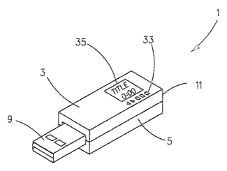
[0034] With reference to Fig. 6, a third embodiment a flash memory drive 1
includes a display screen 35 viewable via top cover 3. Display screen 35 can
be
connected to suitable circuitry mounted on printed circuit board 7 for
providing a
visual indication of the title of the digital audio data, the time remaining
in a song and
other useful and desirable information. This elnbodiment can replace push
button 23
a.nd/or master/slave switch 21 witli buttons 33. Flash memory drive 1 can be
7
CA 02576056 2007-02-05
WO 2006/017553 PCT/US2005/027523
programmed so download/copy logic chip 15 is responsive to the actuation of
one or
more buttons 33 for setting the device to be a master or a slave. A visual
indication of
"Master" or "Slave" can be provided on display screen 33. A signal can also be
sent
to download/copy logic chip 15 to initiate the transfer of data to or from
flash memory
clup 13 when another one of the buttons 33 is pressed. A visual indication
such as
"Transfer in Progress" may be provided on display screen 35, thereby obviating
the
need for LEDs 25a, 25b and 25c. However, display screen 35 and LEDs 25a, 25b
and
25c may also be used together in a single embodiment. Display screen 35 can be
a
liquid crystal display (LCD), a plasma screen or the like.
[0035] With reference to Fig. 7, the present invention is also a method for
transferring data to or from the flash memory chip of a flash memory drive
with
integrated male and female connectors. The method begins at step 61 by
inserting the
male connector of a first flash memory drive into the female comiector of a
second
flash memory drive. Next, at step 63, the first drive is set to master and the
second
drive is set to slave using each of the drive's master/slave switches. Then,
at step 65,
the push button switch is activated to initiate the transfer of data from the
flash
memory chip of the first flash memory drive to the flash memory chip of the
second
flash memory drive. Finally, at step 67, the data is transferred from the
flash memory
chip of the first drive to the flash memory chip of the second drive. The
preceding
method is illustrative of the transfer of data between two flash memory drives
in
accordance with the present invention and is not to be construed as limiting
the
invention. The transfer of data between a flash memory drive in accordance
with the
present invention and prior art flash memory drives, computers, palm devices,
laptops, and the like is also envisioned. For example, when the male connector
of a
prior art flash memory drive is inserted into the female connector of a flash
memory
drive in accordance with the present invention, the master/slave switch of the
flash
memory drive in accordance with the present invention is set to master for
transferring data from the flash memory chip of flash memory drive in
accordance
with the present invention to the flash memory chip of the prior art flash
memory
drive. A further example is wlien the male connector of a flash memory drive
in
accordance with the present invention is inserted into the female connector of
a
computer, palm device and the like, the transfer of data to or from the flash
memory
chip of the flash memory drive in accordance with the present invention can be
controlled by the computer, palm device and the like in a manner known in the
art.
8
CA 02576056 2007-02-05
WO 2006/017553 PCT/US2005/027523
[00361 VJhile the present invention was described with reference to preferred
embodiments of the flash memory drive with integrated male and female
connectors,
those skilled in the art may make modifications and alterations to the present
invention without departing from the scope and spirit of the invention.
Accordingly,
the above detailed description is intended to be illustrative rather than
restrictive. The
invention is defined by the appended claims, and all changes to the invention
that fall
within the meaning and range of equivalency of the claims are to be embraced
by
their scope.
9