Note: Descriptions are shown in the official language in which they were submitted.
CA 02576111 2007-02-05
WO 2006/060041 PCT/US2005/026131
-1-
COATED WATER SOLUBLE NANOPARTICLES
BACKGROUND OF INVENTION
Field of the Invention
The invention relates to nanoparticles and methods for making nanoparticles,
and
in particular, to semiconductor nanocrystals that exhibit improved
hydrophilicity.
Discussion of Related Art
Nanoparticles are microscopic particles of matter having dimensions on the
lo nanometer scale. Of particular interest are a class of nanoparticles known
as
semiconductor nanocrystals, or quantum dots, that exhibit properties that make
them
particularly useful in a variety of applications. Because of quantum
confinement effects,
semiconductor nanocrystals can exhibit size-dependent optical properties. The
particles
give rise to a class of materials whose properties include those of both
molecular and
bulk forms of matter. When these nanoparticles are irradiated, more energy is
required
to promote the electrons to a higher state, leading to an increase in energy
release in the
form of photons and light emission in a color that is characteristic of the
material. The
resulting photons that are released typically exhibit a shorter wavelength
than those
released from a bulk form of the same material. The quantum confinement of
electrons
2o and holes in three dimensions contributes to an increasing effective band
gap with
decreasing nanocrystal size. Therefore, smaller nanocrystals typically exhibit
shorter
emitted photon wavelength. For example, nanocrystals of cadmium selenide
(CdSe) can
emit across the entire visible spectrum when the size of the crystal is varied
over the
range of from two to six nanometers.
Another aspect of semiconductor nanocrystals is that crystals of a uniform
size
typically are capable of a narrow and symmetric emission spectrum regardless
of
excitation wavelength. Thus, if nanocrystals of different sizes are employed,
different
emission colors may be simultaneously obtained from a common excitation
source.
These capabilities contribute to the nanocrystals' potential as diagnostic
tools, for
example, as fluorescent probes in biological labeling and diagnostics. These
nanocrystals, or quantum dots, exhibit high emission stability over long
periods of time,
thus providing advantages over conventional biological probing dyes. One class
of
CA 02576111 2007-02-05
WO 2006/060041 PCT/US2005/026131
-2-
semiconductor nanocrystals are the cadmium chalcogenides. These include, for
example, cadmium selenide and cadmium telluride nanoparticles.
It is known that improved quantum yields of semiconductor nanocrystals can be
obtained by passivating the nanocrystals by reducing the incident of surface
non-
radiative recombination sites. Surface passivation can be achieved, for
example, by
coating a material around the nanocrystals. See, e.g., Alivisatos et al., U.S.
Patent No.
6,255,198. The coatings can be inorganic or organic although inorganically
coated
quantum dots are typically more robust and exhibit less degradation of photo
luminescence quantum yield in solution than do organically passivated quantum
dots.
For semiconductor nanocrystals to be useful in biological applications, it is
preferred that the crystals are water soluble, photo-stable and non-toxic.
Some quantum
dots may exhibit water solubility but are typically not photo-stable and are
toxic. Other
nanocrystals have been coated, for example, with short chain water soluble
molecules,
such as thiols, to render the nanocrystals soluble. However, these organically
coated
quantum dots have been shown to be unstable and exhibit deteriorating photo-
luminescent properties. Others, such as Bawendi et al. in U.S. Patent Nos.
6,319,426 and
6,444,143, hereby incorporated by reference, have synthesized semiconductive
nanocrystals having an organic layer that also includes linking groups for the
attachment
of hydrophilic groups that can provide improved water solubility.
Some have proposed coating nanocrystals using silicate as a precursor. These
methods use silane as a surface primer to deposit a thin shell of silica in
water. The silica
shell can then be thickened using the Stober method. These procedures,
however, are
complicated and time-consuming. Others have used microemulsions as a technique
for
silica coating. In particular, using reverse microemulsions, monodispersed
silica
particles can be synthesized. Encapsulation of nanoparticles within silica can
lead to an
enhancement in chemical stability and photo-stability. This has been done in
nanoparticles having a zinc sulfide (ZnS) core/two photon dye/silica particles
and the
encapsulated dye within the silica shell has exhibited enhanced luminescence
and
lifetime. However, synthesized TOPO semiconductor nanocrystals are water
insoluble
and thus silica cannot be precipitated with the nanocrystals within the
aqueous domains
of the microemulsion.
CA 02576111 2007-02-05
WO 2006/060041 PCT/US2005/026131
-3-
SUMMARY OF INVENTION
The invention is directed, in part, to nanoparticles, soluble nanoparticles
and
metliods for making nanoparticles.
In one aspect, a coated nanoparticle is provided,'the nanoparticle comprising
a
core comprising a semiconductor material, a non-semi-conductor passivation
layer
contacting at least a portion of the core, and a non-organic shell
encapsulating at least
partially the core and the passivation layer.
In another aspect, a method of making a water-soluble nanoparticle is
provided,
the method comprising contacting an amine with a nanoparticle to modify the
nanoparticle surface, suspending the nanoparticle in an aqueous-in-nonaqueous
emulsion, introducing a silica precursor to the emulsion, and polymerizing the
silica
precursor to form a silica shell that at least partially encapsulates the
nanoparticle.
In another aspect, a semiconductor nanocrystal solution is provided, the
solution
comprising an aqueous solution having a pH of less than about 8.0, a plurality
of
semiconductor nanocrystals dissolved in the aqueous solution wherein at least
90% of the
semiconductor nanocrystals, by weight, remain dissolved for greater than 6
hours.
In another aspect, a semiconductor nanocrystal is provided wherein the
nanocrystal is soluble in water at a pH of less than about 8Ø
In another aspect, a nanoparticle is provided, the nanoparticle comprising a
silica
shell encapsulating a core, the silica shell including polyethylene glycol, or
a derivative
thereof.
BRIEF DESCRIPTION OF DRAWINGS
The accompanying drawings, are not intended to be drawn to scale. In the
drawings, each identical or nearly identical component that is illustrated in
various
figures is represented by a like numeral. For purposes of clarity, not every
component
may be labeled in every drawing. In the drawings:
Fig. 1 is a schematic illustration of a silica-coated CdSe semiconductor
nanocrystal.
Fig. 2 is a schematic illustration of a coated nan6crystal with a shell
including
long chain hydrophilic species.
Fig. 3 is a schematic illustration of a nanoparticle including a shell and a
passivation layer.
CA 02576111 2007-02-05
WO 2006/060041 PCT/US2005/026131
-4-
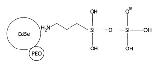
Fig. 4 illustrates a nanoparticle core in contact with an amino silane surface
cap
and a surfactant.
Fig. 5 illustrates a nanoparticle core with exchanging surfactants and a
silica
shell.
Figs. 6a-6c provide a schematic diagram describing the encapsulation of
hydrophobic semiconductor nanocrystals within the aqueous domains of a reverse
microemulsion, using the interaction of hydrophilic groups (polar ends) of two
different
surfactants, TOPO and IGEPAL.
Figs. 7a-7c provide a schematic diagram describing steps that can result in
the
encapsulation of hydrophobic semiconductor nanocrystals (QDs) within a silica
shell.
The steps include micellar collisions, nucleation and polymeric growth of
monomers.
Fig. 8 is a photocopy of a transmission electron micrograph (TEM) of CdSe/ZnS
QD-silica core-shell structures having a diameter of about 6 nm encapsulated
within an
approximately 22 nm silica shell using a microemulsion technique. The majority
of
single QDs are encapsulated within a single silica shell.
Fig. 9 is a photocopy of a transmission electron micrograph (TEM) of CdSe/ZnS
QD-silica core-shell structures having a diameter of about 6 nm encapsulated
within an
approximately 100 nm silica in the microemulsion.
Fig. 10 illustrates graphically the effect of TEOS concentration on silica
shell
thickness and also on the quantum yield (QY) relative to uncoated CdSe/ZnS
nanoparticles.
Fig. 11 shows the absorption and emission spectra of CdSe/ZnS semiconductor
nanoparticles with and without silica coating.
Fig. 12 graphically compares the photo-stability of silica-coated CdSe/ZnS
semiconductor nanocrystals with organic-coated semiconductor nanoparticles.
Figs. 13a-c illustrate the changes of emission intensity of core semiconductor
nanocrystals with various silica coating times. Volume of TEOS (VTEOs) added
into the
microemulsion is indicated.
Fig. 14a shows the relative emission intensity versus coating time at various
3o TEOS concentrations for core semiconductor nanocrystals.
Fig. 14b shows the emission wavelength versus coating time at various TEOS
concentrations for core semiconductor nanocrystals.
CA 02576111 2007-02-05
WO 2006/060041 PCT/US2005/026131
-5-
Fig. 14c shows the relative emission intensity versus TEOS concentrations at 2
hours coating time for core semiconductor nanocrystals.
Figs. 15a-c illustrate the changes of emission intensity of APS-modified core
semiconductor nanocrystals upon various silica coating times. Volume of TEOS
(VTEOS)
added into the microemulsion is indicated.
Fig.16a shows the relative emission intensity versus coating time at various
TEOS concentrations for APS-modified core semiconductor nanocrystals.
Fig. 16b shows the emission wavelength versus coating time at various TEOS
concentrations for APS-modified core semiconductor nanocrystals.
Fig. 16c shows the relative emission intensity versus TEOS concentrations at 8
hours coating time for APS-modified core semiconductor nanocrystals.
Fig. 17a is a photocopy of a high-resolution TEM micrograph of silica-coated
CdSe semiconductor nanocrystals in water.
Fig. 17b shows the EDX mapping of silica-coated CdSe semiconductor
nanocrystals in water.
Fig. 18a shows the photo-stability of CdSe semiconductor nanocrystals coated
with silica in PBS/H2O with and without APS. For comparison, core
semiconductor
nanocrystals in toluene are shown.
Fig. 18b depicts the increase in percentage of Quantum Yield for silica-coated
CdSe Semiconductor nanocrystals relative to the uncoated CdSe semiconductor
nanocrystals in toluene after irradiation with 365 nm excitation for 24 hours.
Fig. 19 graphically illustrates silica coating time vs. quantum yield for
CdSe/ZnS
semiconductor nanocrystals.
Fig. 20 is a photocopy of a micrograph illustrating single cores of CdSe/ZnS
encapsulated within single shells of silica having a diameter of about 25 nm.
Fig. 21 graphically illustrates coating time vs. quantum yield for different
water
concentrations in the microemulsion.
Fig. 22a is a photocopy of a micrograph showing consistent shell thickness,
improved sphericity and improved monodispersity at increasing amounts of TEOS.
Fig. 22b is a bar graph showing improved quantum yield with greater amounts of
TEOS.
CA 02576111 2007-02-05
WO 2006/060041 PCT/US2005/026131
-6-
DETAILED DESCRIPTION
The present invention relates to nanoparticles, and methods of making
nanoparticles, that can exhibit improved quantum yield, and/or improved water
solubility, and/or improved photo-stability, and/or improved photo-
luminescence. The
nanoparticles may include a non-semiconductor and/or non-metallic and/or non-
inorganic passivation layer. The passivation layer may be amorphous, i.e., it
lacks a
crystalline structure. One preferred form of ainorphous passivation layer is
one
comprising a material such as an amino silane. In addition, the nanoparticles
may
include a silica shell that partially or totally eiicapsulates the
nanoparticle core. In some
cases, the silica shell may be derivatized with, for example, polyethylene
glycol (PEG) or
other materials that provide improved characteristics, such as water
solubility.
Nanoparticles of improved quantum yield, stability, solubility and/or
biocompatibility
can lead to improved methods, such as, for example, medical diagnostics.
The term "nanoparticle" is used herein as it is known in the art and typically
refers to particles having a dimension of less of 100 nanometers. One class of
nanoparticles are the "semiconductor nanocrystals" or "quantum dots" that can
provide
unique emission spectra dependent, in part, on the size of the specific
particle.
A "passivation" layer is a material associated with the surface of a
semiconductor
nanocrystal that serves to eliminate energy levels at the surface of the
crystal that may
act as traps for electrons and holes that degrade the luminescent properties
of the
nanocrystal. An example is a ZnS layer surrounding a CdSe semiconductor
nanoparticle.
Passivation layers result in improved quantum yields when compared to
untreated
particles.
An "emulsion" is a dispersion of a non-aqueous solvent and an aqueous solvent.
A "reverse emulsion" or "aqueous in non-aqueous emulsion" is a dispersion of
discrete
areas of aqueous solvent (aqueous phase) within a non-aqueous solvent.
A "shell" is a layer that surrounds or partially surrounds a nanoparticle core
and
in some cases may be chemically bound to the nanoparticle, such as by ionic or
covalent
bonding, and in other cases is not bound to the nanoparticle core. The shell
forms part of
the nanoparticle.
A"surfactant" is a material exhibiting amphiphilic properties and is used
herein
as it is commonly used in the art, e.g., for introducing hydrophobic species
to hydrophilic
environrnents.
CA 02576111 2007-02-05
WO 2006/060041 PCT/US2005/026131
-7-
The term "water soluble" is used herein as it is commonly used in the art to
refer
to the dispersion of a nanoparticle in an aqueous environment. "Water soluble"
does not
mean, for instance, that each material is dispersed at a molecular level. A
nanoparticle
can be composed of several different materials and still be "water soluble" as
an integral
particle.
A "biological fluid" is a fluid present in or obtained from animal or plant
and is
typically aqueous in nature. Biological fluids include, for example, blood,
urine, lymph,
saliva, sweat, and tears.
A "precursor" is a substance that can be transformed into a second substance
that
exhibits different properties from the first. For example, a monomer is a
polymer
precursor if it can be transformed into a polymer.
In one aspect, a nanoparticle includes a shell that encapsulates or partially
encapsulates the nanoparticle. In some embodiments, the shell is not
chemically bound
to the nanoparticle and yet may contain the nanoparticle by encapsulation.
Thus, the
nanoparticle and shell may be devoid of ionic bonds and/or covalent bonds
between the
two. The shell may be non-organic and may be a silicon polymer such as silica.
A non-
organic shell is one that is not based on carbon and polymers of carbon, but
nonetheless
may, in some cases, include carbon atoms.
Fig. 1 shows schematically one embodiment of the invention. Nanoparticle 100
includes a core 110 and a shell 120. Shell 120 can be chemically bound or
unbound to
the core 110. The core can be a semiconductor material such as a semiconductor
nanocrystal (quantum dot). The shell may be generally spherical and may have a
mean
diameter that is about 1.5X, 2X, 5X, 10X or >10X the diameter of the core.
Typically, a
single core is encapsulated by a single shell although in some embodiments,
two or more
cores may be contained within a single shell.
In another aspect of the invention, a semiconductor nanocrystal includes a
passivation layer. In some embodiments, the passivation layer may be of a
material that
is non-conductive and/or non-semiconductive. For example, the passivation
layer may
be of a material that does not exhibit a higher band gap than a nanocrystal
which it
surrounds. In specific embodiments, the passivation layer may be non-ionic and
non-
metallic. A non-conductive material is a material that does not transport
electrons when
an electric potential is applied across the material.
CA 02576111 2007-02-05
WO 2006/060041 PCT/US2005/026131
-8-
FIG. 3 illustrates schematically and not to scale a nanoparticle 200 including
a
core 210, a surface passivation layer 230 and a shell 220. The shell may be
organic or
non-organic and may comprise a non-organic polymer such as silica. In this
embodiment, passivation layer 230 is a non-semiconductor and is preferably an
amino
(NH2) silane, such as aminopropyl trimethoxysilane (APS). The inclusion of
this
passivation layer has been shown to provide a quantum yield of about 10-30% or
10-20%
in aqueous media.
FIG. 4 illustrates schematically an amino silane modifying the surface of a
nanocrystal core to form a passivation layer. The passivation layer can be
comprised of,
1o or consist essentially of, a compound exhibiting a nitrogen-containing
functional group,
such as an amine. The amine may be bound directly or indirectly to one or more
silicon
atoms such as those present in a silane or other silicon polymer. The silanes
may include
any additional functional group such as, for example, alkyl groups, hydroxyl
groups,
sulfur-containing groups, or nitrogen-containing groups. Compounds comprising
the
passivation layer may be of any size but typically have a molecular weight of
less than
about 500 or less than about 300. The preferred class of compounds are the
amino
silanes and in some embodiments, amino propyl trimethoxysilane (APS) can be
used.
The use of APS in semiconductor nanocrystals has been shown to provide
passivation
and to improve quantum yields to a level comparable to the improvements
obtained by
the use of higher band gap passivation layers such as those made of zinc
sulfide (ZnS).
Nanoparticles including a silica shell will, of course, be of greater
dimensions
than a similar nanoparticle absent the shell. For example, nanoparticles of
the invention
may exhibit mean diameters of less than 100 nm, less than 50 nm, or less than
or equal to
about 25 nm. In other embodiments, the mean diameter of the nanoparticle
including the
shell may be greater than 5 nm, greater than 10 nm, greater than 20 nm, or
greater than or
equal to about 25 nm.
In some embodiments, a silica shell can be functionalized or derivatized to
include compounds, atoms, or materials that can alter or improve properties
such as
water solubility, water stability, photo-stability and biocompatibility. For
example, a
silica shell can include moieties such as polyethylene glycol (PEG) and other
glycols.
These nanoparticles, with and without PEG, have been shown to be non-toxic to
living
cells for extended periods, and it is believed that the nanoparticles are also
non-toxic in
CA 02576111 2007-02-05
WO 2006/060041 PCT/US2005/026131
-9-
vivo due, at least in part, to the isolation of the toxic core within the
polymerized silica
shell.
As shown in FIG. 2, a shell 120, that may be non-organic, can include
hydrophilic species 130 that can provide greater hydrophilicity to the
nanoparticle.
Hydrophilic species 130 can be, for example, a polyethylene glycol (PEG) or a
derivative
of polyethylene glycol. Derivatives include, but are not limited to,
functionalized PEGs,
such as amine, thiol and carboxyl functionalized PEG. The hydrophilic species
130 is
associated with the shell 120 and can be chemically bound to the shell 120 or
can be, for
example, physically trapped by the shell material. Preferably, hydrophilic
species 130
1o includes a portion that can be chemically bonded to the shell and a second
portion that
provides hydrophilicity and may extend outwardly from the surface of the
shell.
Presence of these glycols can impart superior water solubility characteristics
to
the nanoparticles while being biocompatible and nontoxic and can, in some
instances,
provide for better dispersion of the nanoparticles in solution. For example,
by
integrating PEG into the silica shell, the semiconductor nanocrystal may be
rendered
water soluble at pHs of less than 8, less than or equal to 7.5, less than or
equal to 7 or less
than or equal to 6.5. Thus, these nanoparticles may be water soluble at
neutral or below
neutral pHs and thus may be biocompatible and appropriate for use in
biological fluids
such as blood and in vivo. In some embodiments, the inclusion of PEG into the
silica
shell provides for a nanoparticle that can remain in solution for a period of
greater than I
hour, greater than 6 hours, greater than 12 hours or greater than 1 day. In
addition, the
presence of PEG or related compounds in the silica shell can provide for a
nanoparticle
exhibiting a reduced propensity to adsorb protein, cells, and other biological
materials.
This means that, for example, when used in vivo, the particles can stay in
solution for a
longer period of time than do similar particles, thus allowing for increased
circulation
and improved deliverability to intended targets.
One embodiment is shown in FIG. 5 that illustrates schematically the formation
of a silica shell 120 around a CdSe core 110. Portions of two surfactants,
TOPO 140 and
IGEPAL 150, are shown. TOPO includes the hydrophilic group phosphine oxide and
IGEPAL includes the hydrophilic group PEO. The source of the IGEPAL 150 is the
reverse microemulsion (aqueous in non-aqueous) and the source of the TOPO is
the
TOPO capped semiconductor nanocrystal. FIGs. 6a-6c illustrate how the reverse
micelles can present the nanocrystal cores for encapsulation at the water/oil
interface.
CA 02576111 2007-02-05
WO 2006/060041 PCT/US2005/026131
-10-
Thus, while the nanocrystals may be transported to the aqueous phase, the
formation of
the silica polymer tends to occur around the nanocrystals at the aqueous/non-
aqueous
interface. FIGs. 7a-7c illustrate the formation of a silica shell around a
nanoparticle core
at the oil/water (cyclohexane/water) interface.
The aqueous in non-aqueous microemulsion can be produced using a variety of
non-polar solvents. Preferably the non-polar solvent is a hydrocarbon and may
be an
aliphatic hydrocarbon and in a more preferred embodiment is a non-aromatic
cyclic
hydrocarbon such as cyclopentane, cyclohexane or cycloheptane.
In one embodiment, a semiconductor nanocrystal including a core of a cadmium
chalcogenide is coated with a passivation layer comprising an amine. The core,
that may
include cadmium selenide or cadmium telluride, for example, can be made using
methods known to those skilled in the art. An aqueous in non-aqueous reverse
micro
emulsion can be prepared, using for example, an ionic or non-ionic surfactant.
Non-ionic
surfactants include, for example, polyphenyl ethers, such as IGEPAL CO-520,
while
ionic surfactants include, for example, dioctyl sulfosuccinate sodium salt
(AOT). As
conventionally prepared, the calcium chalcogenide core is typically presented
with a
trioctyl phosphine oxide (TOPO) surfactant. TOPO includes a hydrophilic end
comprising phosphine oxide while IGEPAL includes a hydrophilic end comprising
polyoxyethylene (PEO). After introduction of the TOPO semiconductor
nanocrystals
into the reverse emulsion, the TOPO can be partially or completely exchanged
for
IGEPAL due, in part, to the much higher concentration of IGEPAL in the reverse
emulsion.
Upon the exchange of TOPO for IGEPAL, the semiconductor nanocrystal cores
are amenable to the aqueous domains in the reverse emulsion and a sol-gel
precursor,
such as tetraethylorthosilicate (TEOS) can be polymerized using methods known
to those
skilled in the art, around the core to produce a silica shell. The resulting
nanostructure
includes a core of a cadmium chalcogenide, a passivation layer of an amino
silane such
as APS and a hydrophilic shell, such as a shell of polymerized silica.
Surfactants other
than IGEPAL may be used and may be varied, in part, depending upon the core
material,
how the nanoparticle core is capped and the reverse emulsion that is used.
Preferred
surfactants are those that can be exchanged for TOPO or other surfactants that
are used
to cap the core and that also provide enough hydrophilicity to draw the core
into aqueous
CA 02576111 2007-02-05
WO 2006/060041 PCT/US2005/026131
-11-
portions of the micro-emulsion, thus providing an environment for the
formation of the
silica shell.
In another aspect, a method of making a nanoparticle including a silica shell
modified to improve biocompatibility and/or water solubility is provided. For
example,
in some embodiments a PEG modified silica shell can be formed around a
nanoparticle.
The nanoparticle core may be a semiconductor nanocrystal or other
nanoparticle. As
described above, the nanoparticle core may be introduced into a reverse micro-
emulsion
(aqueous in non-aqueous emulsion) to prepare it for encapsulation. In another
step, a
base such as ammonia (NH4OH) including a glycol such as polyethyleneglycol
monomethylether (PEG-m) can be dissolved into the microemulsion. The PEG may
be
of any molecular weight, but it is preferably of a molecular weight of greater
than 1,000
and less than 20, 000 and in some embodiments, is in a range of between 5,000
and
10,000. A sol-gel precursor such as TEOS can then be added and the mixture can
be
stirred allowing the PEG to be incorporated into the forming silica shell. The
resulting
silica shell derivatized with PEG can provide for improved quantum yield,
improved
water solubility, improved biocompatibility in a reduced propensity to
coagulate.
In one embodiment, ammonia and PEG are stirred into the microemulsion before
a sol-gel precursor such as TEOS is added. After addition of the sol-gel
precursor, the
microemulsion can be stirred continuously until a preferred amount of silica
polymerization has taken place. During this time, the PEG is incorporated into
the silica
shell and can alter the properties of the silica shell by, for example,
increasing
hydrophilicity, altering the nanoparticle's propensity to adsorb materials
such as proteins
in cells, and can increase repulsion forces between particles, providing for
an extended
period of suspension of the particles without coalescing;
The amount of water (29.5% aqueous NH4OH) in the aqueous in non-aqueous
(reverse) microemulsion can be varied based upon the specific reaction that is
desired.
For example, in some embodiments the amount of water in the reverse
microemulsion is
between 0.2 and 0.5 percent by volume. In preferred embodiments, the amount of
water
is between 0.3 and 0.4 percent by volume and in some embodiments it has been
found
that quantum yield can be maximized when the amount of water in the reverse
microemulsion is about 0.3 percent by volume.
The amount of sol-gel precursor added to the microemulsion can also affect the
properties of the nanoparticle. For example, while an increase in the amount
of sol-gel
CA 02576111 2007-02-05
WO 2006/060041 PCT/US2005/026131
-12-
precursor does not appear to increase the shell thickness, an increase in the
amount of
sol-gel precursor does appear to improve this sphericity as well as the
monodispersity of
the particles. In some embodiments, quantum yield is also improved with higher
concentrations of sol-gel precursor. For example, see Figs. 20A and 20B.
EXAMPLES
Example 1
Preparation of Silica-Coated ZnS-capped CdSe nanocrystals (CdSe/ZnS/SiO2) in
Reverse Microemulsion (aqueous in non-aqueous emulsion)
CdSe/ZnS semiconductor nanocrystals with excess TOPO without any surface
modification were prepared according to literature procedures (Hines et al.,
"Synthesis
and Characterization of Strongly Luminescing ZnS-Capped CdSe Nanocrystals" J.
Phys.
Chem. 100, 468-471, 1996. Dabbousi et al., "(CdSe)ZnS Core-Shell Quantum Dots:
Synthesis and Characterization of a Size Series of Highly Luminescent
Nanocrystallites"
J. Phys. Chem. B 101, 9463-9475, 1997.). The particles had luminescence
quantum
yields of 10-25% and emission at 625 nm (F)vVHM = 30 nm). The particles were
precipitated once from methanol to remove excess TOPO and trioctylphosphine
oxide
(TOP). Inverse micelles were prepared using a non-ionic surfactant such as
Igepal CO-
520 and cyclohexane as solvent.
Figs. 6 and 7 depict the schemes of the transformation of hydrophobic
semiconductor nanocrystal into aqueous domains of the reverse microemulsion
and silica
coating, respectively. Typically, core-shell semiconductor nanocrystals
passivated with
TOPO and dissolved either in butanol or n-hexane were injected into the
reverse
micelles. This was followed by the addition of TEOS and was allowed to stir
for 1 hour.
Addition of ammonia resulted in a stable water-in-oil reverse microemulsion.
The
resulting solution was stirred for 24 hours, which resulted in homogeneous
silica
deposition. Due to the large excess of Igepal, the TOPO ligand was exchanged
for
Igepal in cyclohexane and the semiconductor nanocrystals became more
hydrophilic.
The nanocrystals were then solubilized by water through exchange of the Igepal-
capped
semiconductor nanocrystals with Igepal-capped aqueous domains.
CA 02576111 2007-02-05
WO 2006/060041 PCT/US2005/026131
- 13 -
Example 2
TEM Characterization of Silica-Coated ZnS-capped CdSe nanocrystals
(CdSe/ZnS/SiO2) in Reverse Microemulsion
Electron microscopy revealed that the majority (>90%) of nanocrystals are
encapsulated as single particles within a silica shell (Figure 8). The average
total
diameter of nanocrystal/Silica is - 22 nm. Figure 9 shows the encapsulation of
nanocrystals within ca. 100 nm silica in the reverse microemulsion. Varying
the amount
1o of water and ammonia in the microemulsion also affects the shell thickness,
since this
alters the aqueous domain size. The silica shell thickness can be increased by
increasing
the TEOS concentration as shown in Figure 10. The higher the concentration of
TEOS
the larger is the silica diameter. Increase in the size of silica lowers the
emission
intensity and QY. The total diameter of coated nanocrystals affect the QY
relative to the
uncoated nanocrystals, which is also shown in Figure 10.
Example 3
Emission Characteristics of Silica-Coated ZnS-capped CdSe nanocrystals
(CdSe/ZnS/SiO2) in Water
Silica-coated nanocrystals in the microemulsion were centrifuged at 18000 rpm
for 30 minutes and the pellet was washed with cyclohexane twice and dispersed
in an
alkaline aqueous solution of pH 8-9. The silica-coated nanocrystals in water
were
characterized by UV-visible absorption spectroscopy and fluorescence
spectroscopy.
Figure 11 shows the absorption and fluorescence spectra of the CdSe
nanocrystals before
and after silica coating. UV-visible and photoluminescence spectra show that
there is a
5nm red-shift for CdSe/ZnS/SiO2 in water, in comparison to the CdSe/ZnS
nanocrystals
in the parent solution, butanol. Silica-coated semiconductor nanocrystals in
water
showed remarkable colloidal stability over a period of several months.
Silica-coated nanocrystals showed remarkable photostability. The nanocrystals
in water and in butanol were exposed to UV irradiation (335 nm cut-off
filter). About
85% of the quantum yield was retained after 24 hours for the coated particles
in water,
CA 02576111 2007-02-05
WO 2006/060041 PCT/US2005/026131
-14-
where as the parent semiconductor nanocrystal solution virtually lost all
luminescence
after 24 hours. We also compared the results with those dots in water capped
by
mercaptoundecanoic acid (MUA). MUA-capped semiconductor nanocrystals in water
exhibited initial photo-brightening and then photo-dissolution over a period
of 24 hours.
The exciton absorption peak position is plotted against time of photolysis in
Figure 12.
The peak position remains constant at 616 nm for silica-coated semiconductor
nanocrystals, indicating that the dots are photostable over extended periods
of photolysis
time. On the contrary, the nanocrystals capped with MUA show photo-dissolution
as
exemplified by blue-shifts in the exciton position over 24 hours of
photolysis.
Example 4
Preparation of TOPO-capped CdSe semiconductor nanocrystals and Interaction of
Surfactants in IGEPAL Reverse Micelles
The following experiment was run to demonstrate that the TOPO on a TOPO
capped nanocrystal could be exchanged for a more hydrophilic surfactant that
can alter
the hydrophilicity of the nanoparticle.
CdSe semiconductor nanocrystals with excess TOPO without any surface
modification were prepared according to literature procedures (Peng et al.,
"Formation of
High-Quality CdTe, CdSe, and CdS Nanocrystals Using CdO as Precursor" J. Am.
Chem. Soc. 123, 183-184, 2001). The particles had luminescence quantum yields
of 10-
20% and emissions at 550-600 nm (FWHM = 30-40 nm). The particles were
precipitated once from methanol to remove excess TOPO and trioctylphosphine
oxide
(TOP). Inverse micelles were prepared using the non-ionic surfactant IGEPAL CO-
520
(polyoxyethylene nonylphenyl ether), at 5%, by weight, and cyclohexane as
solvent.
Emission experiments showed that TOPO-capped nanocrystals were exchanged
by IGEPAL. Changes in emission intensity and emission wavelength for
nanocrystals in
IGEPAL micelles in comparison with those nanocrystals in cyclohexane are due
to the
surface ligand exchange reactions between TOPO and IGEPAL.
CA 02576111 2007-02-05
WO 2006/060041 PCT/US2005/026131
-15-
Example 5
Preparation of Silica-Coated Nanocrystals (CdSe/SiO2) in IGEPAL Reverse
Microemulsion (aqueous in non-aqueous emulsion)
CdSe nanocrystals passivated with TOPO were precipitated with methanol once
and the precipitate was dried under nitrogen in order to remove the methanol.
To the
precipitate, cyclohexane was added and vortexed until the solution became
clear. The
semiconductor nanocrystals were introduced into the reverse micelles of an
aqueous in
non-aqueous emulsion made with 0.5 g IGEPAL and 10 ml cyclohexane, and stirred
for
30 minutes. Then 100 l of 29.5% NH4OH was added and stirred for another 1
hour.
Finally, TEOS was added at different concentrations and the stirring continued
for 24
hours. Aliquots of samples were taken at different periods of coating times
ranging from
1 to 24 hours, and emission spectra were recorded.
Figures 13a-13c depict the effect of TEOS concentration and silica coating
time
on the emission characteristics. For comparison, the emission spectra of
nanocrystals in
IGEPAL micelles (no silica coating) are shown. It is clear that the full width
at half
maximum (FWHM) of the emission peak is increased with an increase in coating
time.
In Figure 14a the relative emission intensity is plotted against coating time
at various
TEOS concentration. Results show that the emission intensity increases at 2
hours of
silica coating after an initial decrease at 1 hour, and that a further
increase in coating time
at 4 hours decreases the emission intensity, which remains saturated with
further increase
in coating time. The initial increase in the intensity at 2 hours is
apparently due to silica
formation when ammonia adsorption occurs on the surface sites of the
nanocrystals. The
decrease in emission intensity is presumably due to the acidity of the silanol
groups that
quench ammonia basicity by a desorption process at higher coating times
(Figure 14a).
Figure 14b shows the effect of coating time on the emission wavelength at
different TEOS concentrations and different particles sizes. In all the cases,
silica-
coated nanocrystals exhibit a blue shift in comparison with naked (uncoated)
dots. This
implies that IGEPAL-capped nanocrystals are exchanged for silica-coated
nanocrystals.
The surface exchange reaction accounts for the blue shift. The best conditions
for silica
coating are found to employ 5 l TEOS in a total volume of 10 ml microemulsion
and 2
hours of coating time (Figure 14c).
CA 02576111 2007-02-05
WO 2006/060041 PCT/US2005/026131
-16-
Example 6
Preparation of Silica-Coated Nanocrystals (CdSe/SiO2) in IGEPAL Reverse
Microemulsion with an amino silane, APS, Added
CdSe semiconductor nanocrystals passivated. with TOPO were precipitated with
methanol once and the precipitate was dried under nitrogen in order to be free
from
methanol. 2 L of APS were added to the precipitate, which was dissolved in 1
ml of
cyclohexane and vortexed until the solution became clear. APS-modified
nanocrystals
were introduced into the reverse micelles and stirred for 30 minutes. 100 l
of 29.5 10
NH4OH was the added and stirred for another 1 hour. Finally, 5-20 l TEOS was
added
and the stirring continued for 24 hours. Aliquots of samples were taken at
different
periods of coating times ranging from 1 to 24 hours and emission spectra were
recorded
for samples from each aliquot (Figures 15a-15c).
The results show that APS modification provides more surface passivation than
is
found in the naked dots. The APS modification is preferably done before
injecting the
nanocrystals into IGEPAL reverse micelles. With silica coating, there is no
initial
decrease in the emission intensity at lower TEOS concentrations (FIGs. 15a and
15b),
but there is a decrease at higher concentrations (FIG 15c). At 8 hours of
coating time,
the emission intensity remains higher than all other coating times up to 24 h.
The
comparison of the emission intensities at 8 and 24 hours shows a negligible
decrease
(Figure 16a) irrespective of TEOS concentration. This is believed to occur
because the
amine groups provide additional surface passivation for the APS-modified
nanocrystals
in comparison to the similar nanocrystals absent the APS modification.
Furthermore, the
acidity of the silanol groups that are formed during extended periods of
silica coating
does not seem to affect the emission properties as the amine protects the
nanocrystal
surface.
Figure 16b illustrates the effect of coating time on the emission wavelength
for
different TEOS concentrations and different particles sizes of APS-modified
nanocrystals. Although silica-coated nanocrystals exhibit a blue shift (5-10
nm) in
comparison with naked (uncoated) nanocrystals at different coating times and
various
TEOS concentrations, the observed blue shifts are small compared to those for
CA 02576111 2007-02-05
WO 2006/060041 PCT/US2005/026131
-17-
unmodified nanocrystals (10-20 nm) as shown in Figure 13b. From this data,
good
conditions for silica coating are found to be 2 l TEOS and 8 hours of coating
time
(Figure 16c).
Example 7
TEM Characterization of Silica-Coated Nanocrystals (CdSe/SiO2) in Water
The silica-coated colloidal solution was centrifuged at 12000 rpm for 20
minutes
and the resulting pellet was washed with deionized water twice and dispersed
in a
mixture of water and phosphate buffered saline (PBS). Figure 17a shows the
HRTEM
image of silica-coated nanocrystals in water. The lattice fringes of CdSe are
marked by
arrows. The energy dispersive analysis of X-rays (EDX) mapping (Figure 17b)
confirms
the presence of all elements that are predicted: Cd, Se from CdSe
semiconductor
nanocrystal core, Si, 0 from Si02 shell and P from TOPO. Sulfur impurity,
possibly
from surfactant, is also seen.
Example 8
Photo-stability of Silica-Coated Nanocrystals (CdSe/SiO2) in Water
Figure 18a shows the photo-stability of three different semiconductor
nanocrystals. Included are silica-coated nanocrystals without APS and silica-
coated
nanocrystals with APS, both in a mixture of water and phosphate buffered
saline (PBS).
The third nanocrystal is an uncoated nanocrystal (no silica) in toluene. As
can be seen,
the coated dots exhibited superior photo-stability than did the uncoated ones.
The
increase in QY relative to the uncoated nanocrystals in toluene is believed to
be due to
the photo-brightening of silica-coated nanocrystals. This may be caused by the
photo-
ionization of the nanocrystals. An approximately three-fold increase in QY for
silica-
coated nanocrystals with APS modification before coating, compared to silica-
coated
nanocrystals without APS modification, is clearly seen in Figure 18b.
CA 02576111 2007-02-05
WO 2006/060041 PCT/US2005/026131
-18-
Example 9
Preparation of PEG-Silica-Coated nanocrystals (CdSe/ZnS/SiO2 and CdSe/SiO2) in
IGEPAL Reverse Microemulsion with No APS Added
CdSe/ZnS and CdSe nanocrystals passivated with TOPO were precipitated with
methanol once and the precipitate was dried under nitrogen in order to be free
from
methanol. To the precipitate, cyclohexane was added and vortexed until the
solution
became clear. The nanocrystals were introduced into an aqueous in non-aqueous
emulsion, as described above, and stirred for 30 minutes. 50 l NH4OH
containing
polyethylene glycol monomethyl ether (PEG-m) concentration of 0.05 g/ml NH4OH,
was
added and stirred for another 1 hour. Finally, TEOS was added at different
amounts and
the stirring continued for 144 hours. Aliquots of samples were taken at
different periods
of coating times ranging from 24 to 144 hours. The samples were then
transferred to
water, and the resulting suspensions remained stable, even after 3 weeks. The
enhanced
solubility is attributed to the repulsion force and solvation layer provided
by the PEG.
The quantum yield associated with different coating times was also recorded.
Figure 19 illustrates the effect of silica coating time of CdSe/ZnS
nanocrystals on
the quantum yield of the samples. The quantum yield is plotted against coating
time.
The results show that the emission intensity increases to a maximum after 90
hours of
silica coating. The maximum quantum yield (17%) achieved is greater than that
of the
pre-coated CdSe/ZnS (10%). This is attributed to enhanced surface passivation
by the
silica coating layer surface moiety.
Figure 20 provides an electron micrograph showing that the CdSe/ZnS is
encapsulated as single particle within a silca shell of diameter - 25nm.
Varying the
amount of water (0.3% to 0.4%) in the microemulsion does not appear to affect
the shell
thickness but does appear to decrease the quantum yield (Figure 21). Varying
the
volume of TEOS added (20-60 l) does not appear to affect the shell thickness
but does
seem to improve the sphericity and monodispersity of the particles, as well as
the
quantum yield, as evidenced by Figures 22a and 22b.
While several embodiments of the present invention have been described and
illustrated herein, those of ordinary skill in the art will readily envision a
variety of other
means and/or structures for performing the functions and/or obtaining the
results and/or
CA 02576111 2007-02-05
WO 2006/060041 PCT/US2005/026131
-19-
one or more of the advantages described herein, and each of such variations
and/or
modifications is deemed to be within the scope of the present invention. More
generally,
those skilled in the art will readily appreciate that all parameters,
dimensions, materials,
and configurations described herein are meant to be exemplary and that the
actual
parameters, dimensions, materials, and/or configurations will depend upon the
specific
application or applications for which the teachings of the present invention
is/are used.
Those skilled in the art will recognize, or be able to ascertain using no more
than routine
experimentation, many equivalents to the specific embodiments of the invention
described herein. It is, therefore, to be understood that the foregoing
embodiments are
presented by way of example only and that, within the scope of the appended
claims and
equivalents thereto, the invention may be practiced otherwise than as
specifically
described and claimed. The present invention is directed to each individual
feature,
system, article, material, kit, and/or method described herein. In addition,
any
combination of two or more such features, systems, articles, materials, kits,
and/or
methods, if such features, systems, articles, materials, kits, and/or methods
are not
mutually inconsistent, is included within the scope of the present invention.
All definitions, as defined and used herein, should be understood to control
over
dictionary definitions, definitions in documents incorporated by reference,
and/or
ordinary meanings of the defined terms.
The indefinite articles "a" and "an," as used herein in the specification and
in the
claims, unless clearly indicated to the contrary, should be understood to mean
"at least
one."
The phrase "and/or," as used herein in the specification and in the claims,
should
be understood to mean "either or both" of the elements so conjoined, i.e.,
elements that
are conjunctively present in some cases and disjunctively present in other
cases. Other
elements may optionally be present other than the elements specifically
identified by the
"and/or" clause, whether related or unrelated to those elements specifically
identified.
Thus, as a non-limiting example, a reference to "A and/or B" can refer, in one
embodiment, to A only (optionally including elements other than B); in another
embodiment, to B only (optionally including elements other than A); in yet
another
embodiment, to both A and B (optionally including other elements); etc.
As used herein in the specification and in the claims, unless clearly
indicated to
the contrary, "or" should be understood to have the same meaning as "and/or"
as defined
CA 02576111 2007-02-05
WO 2006/060041 PCT/US2005/026131
-20-
above. For example, when separating items in a list, "or" and "and/or" each
shall be
interpreted as being inclusive, i.e., the inclusion of at least one, but also
including more
than one, of a number or list of elements, and, optionally, additional
unlisted items. In
general, the term "or" as used herein shall only be interpreted as indicating
exclusive
alternatives (i.e. "one or the other but not both") when preceded by terms of
exclusivity,
such as "only one of' or "exactly one of."
As used herein in the specification and in the claims, the phrase "at least
one," in
reference to a list of one or more elements, should be understood to mean at
least one
element selected from any one or more of the elements in the list of elements,
but not
necessarily includiing at least one of each and every element specifically
listed within the
list of elements and not excluding any combinations of elements in the list of
elements.
This defmition also allows that elements may optionally be present other than
the
elements specifically identified within the list of elements that the phrase
"at least one"
refers to, whether related or unrelated to those elements specifically
identified. Thus, as
a non-limiting example, "at least one of A and B" (or, equivalently, "at least
one of A or
B," or, equivalently "at least one of A and/or B") can refer, in one
embodiment, to at
least one, optionally including more than one, A, with no B present (and
optionally
including elements other than B); in another embodiment, to at least one,
optionally
including more than one, B, with no A present (and optionally including
elements other
than A); in yet another embodiment, to at least one, optionally including more
than one,
A, and at least one, optionally including more than one, B (and optionally
including other
elements); etc.
It should also be understood that, unless clearly indicated to the contrary,
in any
methods claimed herein that include more than one act, the order of the acts
of the
method is not necessarily limited to the order in which the acts of the method
are recited.
In the claims, as well as in the specification above, all transitional phrases
such as
"comprising," "including," "carrying," "having," "containing," "involving,"
"holding,"
and the like are to be understood to be open-ended, i.e., to mean including
but not limited
to. Only the transitional phrases "consisting of' and "consisting essentially
of' shall be
closed or semi-closed transitional phrases, respectively, as set forth in the
United States
Patent Office Manual of Patent Examining Procedures, Section 2111.03.
What is claimed is: