Note: Descriptions are shown in the official language in which they were submitted.
CA 02576281 2007-02-06
WO 2006/046983 PCT/US2005/025770
METHOD AND APPARATUS FOR PREVENTING OVERHEATING IN AN
ELECTRONICALLY COMMUTATED MOTOR ASSEMBLY
TECHNICAL FIELD
[00011 This patent relates generally to electric motors and more particularly
to method and
apparatus for preventing overheating in an electronically commutated motor
assembly.
BACKGROUND
[00021 A switched reluctance motor is an electrical motor that includes a
rotor and a stator.
Torque in a reluctance motor is produced by the tendency of the rotor to move
to a position
relative to the stator in which the reluctance of a magnetic circuit is
minimized, i.e. a position
in which the inductance of an energized stator winding is maximized. In a
switched
reluctance motor, circuitry is provided for detecting the angular position of
the rotor and
sequentially energizing phases of the stator windings as a function of rotor
position.
[0003] Switched reluctance motors are doubly salient motors having poles on
both the
stator and the rotor, with windings only on the stator poles. The rotor of a
switched
reluctance motor does not include commutators, permanent magnets, or windings.
Switched
reluctance motors have a variety of uses, including vacuum cleaners, for
example.
[0004] Torque may be produced by energizing or applying current to the stator
windings of
the stator poles associated with a particular phase in a predetermined
sequence. The
energization of the stator windings is typically synchronized with the
rotational position of
the rotor. A magnetic force of attraction results between the poles of the
rotor and the
energized stator poles associated with a particular phase, thereby causing the
rotor poles to
move into alignment with the energized stator poles.
[0005] In typical operation, each time a stator winding of the switched
reluctance motor is
energized, magnetic flux flows from the energized stator poles associated with
a particular
phase, across an air gap located between the stator poles and the rotor poles.
Magnetic flux
generated across the air gap between the rotor poles and the stator poles
produces a magnetic
field in the air gap that causes the rotor poles to move into alignment with
the energized
stator poles associated with a particular phase, thereby producing torque. The
amount of
magnetic flux and, therefore, the amount of torque generated by the switched
reluctance
motor is dependent upon many variables such as, for example, the magnetic
properties of the
material of the rotor poles and the stator poles, and the length of the air
gap between the rotor
poles and the stator poles.
1
CA 02576281 2011-02-01
64267-1454
[0006] The magnetic flux generated can be divided into a main torque-
producing flux and leakage flux. The main flux is the flux that flows through
the
rotor poles and the excited stator poles. This main flux produces a torque on
the
rotor that will tend to align the rotor poles through which the flux passes
with the
excited stator poles. Leakage flux is undesirable in switched reluctance
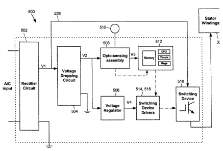
motors
because it directly reduces torque production. More specifically, leakage flux
causes the motor to produce a torque in a direction that is opposite to the
direction
of rotation of the rotor, also known as a braking torque. It is known that
modifications to the rotor pole face may affect torque production in the
switched
reluctance motor.
[0007] Control circuits for switched reluctance motors are generally located
in close proximity to various mechanical components of the motors, often close
to
the rotors, stators, etc. The functioning of the switched reluctance motors
produce
substantial amounts of heat, which can raise the temperature of various
components surrounding the rotor and stator to substantially high levels. As
it is
well known, control circuits for switched reluctance motors almost invariably
use
various electronic components such as integrated circuits, transistors, etc.,
that
are highly sensitive to temperature. Generally, electronic components are
designed to function properly only within a specified operating temperature
range
and if their operating temperature increases or decreases beyond such
specified
operating range, the electronic components may malfunction and/or be
permanently damaged.
[0008] Various methods of cooling are employed to reduce the temperature
surrounding the mechanical components of switched reluctance motors, including
fan, water cooling, etc. While employing such cooling methods may reduce risk
of
damage to the control circuits placed in close proximity to switched
reluctance
motors, there is still a possibility that in certain conditions, the excessive
heat
generated by the switched reluctance motor will damage at least some of the
components of such control circuit. Therefore, it is necessary to employ a
technique to avoid damage to the switched reluctance motor control circuits
from
excessive heat generated by the switched reluctance motor.
2
CA 02576281 2011-02-01
64267-1454
SUMMARY
According to one aspect of the present invention, there is provided a
method of operating a motor apparatus, the motor apparatus having a control
circuit, a rotor and a stator having a stator winding, the control circuit
having a
voltage regulator supplying power to the stator winding via a switching device
and
a micro-controller controlling the switching device, the method comprising:
measuring a temperature of the motor apparatus; comparing the measured
temperature with a threshold temperature; turning off the voltage regulator if
the
measured temperature exceeds the threshold temperature; and preventing a
restart of rotation of the rotor, each time the voltage regulator is turned
off in
response to the measured temperature exceeding the threshold temperature,
absent a recycling of power to the motor apparatus.
According to another aspect of the present invention, there is
provided a control circuit for operating a motor having a rotor and a stator,
the
stator having a stator winding, the control circuit comprising: a switching
device
controlling a power supply to the stator winding; a switching device driver
controlling the operation of the switching device; a voltage regulator circuit
connected to the switching device driver; a micro-controller connected to the
switching device driver; a temperature sensing device adapted to sense the
temperature of the voltage regulator circuit; and a thermal shutdown device
adapted to shutdown the voltage regulator circuit in response to the
temperature
of the voltage regulator being above a threshold level while retaining power
to the
micro-controller to prevent a restart of the motor, absent a recycling of
power to
the motor.
BRIEF DESCRIPTION OF THE DRAWINGS
[0009] The present patent is illustrated by way of examples and not
limitations in the accompanying figures, in which like references indicate
similar
elements, and in which:
2a
CA 02576281 2007-02-06
WO 2006/046983 PCT/US2005/025770
[0010] FIG. 1 is a perspective view of a switched reluctance motor, including
a stator and a
rotor;
[0011] FIG. 2 is a sectional view of the motor shown in FIG. 1;
[0012] FIG. 3 is a cross-sectional view of a stator core of the motor shown in
FIG. 1;
[0013] FIG. 4 is a perspective view of one of a plurality of bobbins
associated with the
stator of the motor shown in FIG. 1, including a plurality of wire retainers
located at an upper
portion of each of the plurality of bobbins;
[0014] FIG. 5 is a top view of an upper housing unit of the motor, including a
second
plurality of mounting elements for receiving an upper portion of each of the
plurality of
bobbins of the stator;
[0015] FIG. 6 is an enlarged perspective view of one of the second plurality
of mounting
elements shown in FIG. 5;
[0016] FIG. 7 is an exploded perspective view of the stator and the upper
housing unit
before assembly;
[0017] FIG. 8 is a perspective view of the stator mounted to the upper housing
unit after
assembly;
[0018] FIG. 9 is a view of the rotor of the motor shown in FIG. 1;
[0019] FIG. 10 is a cross-sectional view of the rotor of the motor shown in
FIG. 1 disposed
within an inner region of the stator core;
[0020] FIG. 11 is an enlarged partial view of a pole of a prior art rotor
approaching a stator
pole;
100211 . FIG. 12 is an enlarged partial view of a rotor pole of the motor
shown in FIG. 1
approaching a stator pole;
[0022] FIGs. 13A-13B are partial views of a rotor pole of the motor shown in
FIG. 1 as the
it approaches the stator pole in a clockwise direction;
[0023] FIG. 14 is a top view of a lower housing unit of the motor shown in
FIG. 1,
including a first plurality of mounting elements for receiving a lower portion
of each of the
plurality of bobbins of the stator in accordance with one embodiment;
3
CA 02576281 2007-02-06
WO 2006/046983 PCT/US2005/025770
[0024] FIG. 15 is a top perspective view of the stator of the motor shown in
FIG. 1
mounted to the lower housing unit;
[00251 FIG. 16 is a top view of the stator and the rotor of the motor shown in
FIG. 1
mounted to the lower housing unit;
[0026] FIG. 17 is a perspective view of an insulating member, including a
first plurality of
mounting elements for receiving a lower portion of each of the plurality of
bobbins of the
stator in accordance with another embodiment;
[0027] FIG. 18 is a top view of the insulating member shown in FIG. 17;
[0028] FIG. 19 is a bottom view of the insulating member shown in FIG. 17;
[0029] FIG. 20 is side view of the insulating member shown in FIG. 17;
[0030] FIG. 21 is a perspective view of one of the plurality of bobbins of the
motor shown
in FIG. 1 disposed within the one of the first plurality of mounting elements
of the insulating
member shown in FIG. 17;
[0031] FIG. 22 illustrates a block diagram of a control circuit for the
switched reluctance
motor;
[0032] FIG. 23 illustrates a circuit diagram of the control circuit
corresponding to the block
diagram of FIG. 22;
[0033] FIG. 24 illustrates a circuit diagram.of an optical sensor assembly
used in the
control circuit of FIG. 22;
[0034] FIG. 25 illustrates a block diagram of a voltage regulator used in the
control circuit
of FIG. 22; and
[0035] FIG. 26 illustrates a flowchart for operating the brushless motor using
the control
circuit of FIG. 22;
[0036] FIGs. 27A and 27B illustrate some of the steps used to synchronize the
switching or
commutation of the power provided to the stator windings;
[0037] FIG. 28 illustrates a start-up wave form in a slow mode for the first
1.5 rotor
revolutions for the switched reluctance motor;
[0038] FIG. 29 also illustrates a number of wave forms in the slow mode
routine;
[0039] FIGs. 30 and 31 illustrate wave forms in the fast mode routine;
4
CA 02576281 2007-02-06
WO 2006/046983 PCT/US2005/025770
[0040] FIG. 32 illustrates some of the steps used to ensure the legitimacy of
a signal
received from a rotor position sensor in the switched reluctance motor; and
[0041] FIG. 33 illustrates three wave forms received from the rotor position
sensor in the
switched reluctance motor.
DETAILED DESCRIPTION OF THE EXAMPLES
[0042] Referring to FIGs. 1-2, a switched reluctance motor 10 may be
constructed as a
package or unit of subassemblies, each of which may be separately preassembled
and
combined together during a manufacturing process. Specifically, the motor 10
may include
an upper housing unit 12, a lower housing unit 13, a stator 14, a rotor 16, a
drive assembly
18, a first end cap 20, and a second end cap 22. Both the upper housing unit
12 and the lower
housing unit 13 may be annular in shape, with the first end cap 20 being
coupled to the upper
housing unit 12, and the second end cap 22 being coupled to the lower housing
unit 13. As
shown in FIGs. 1-2, each of the upper housing unit 12, the lower housing unit
13, the stator
14, the rotor 16, the drive assembly 18, the first end cap 20, and the second
end cap 22 may
be combined into a single package or unit.
[0043] The upper housing unit 12 may include a plurality of apertures 24 for
receiving a
plurality of fasteners 26 to secure the upper housing unit 12 to the stator 14
during assembly.
It should be understood, however, that the upper housing unit 12 may be
secured to the stator
14 in any other suitable manner such as, for example, by a clamp, a mounting
bracket/flange,
or the like.
[0044] Referring to FIG. 3, the stator 14 may be constructed in a square-type
configuration, with slanting or chamfered portions 27 at the four corners of
the stator 14. It
should be understood, however, that the stator 14 may have other
configurations as well such
as, for example, a circular configuration, an oval configuration, a
rectangular configuration,
or the like.
[0045] The stator 14 includes a stator core 28, a plurality of equally spaced
stator poles 30,
and stator windings 32 (FIGs. 7-8 and 10) disposed on the stator core 28. The
stator core 28
includes an inner surface that defines a central bore 34. The stator core 28
may be stamped
or formed from a plurality of laminated sheets, or laminations, of
ferromagnetic material such
as, for example, steel. Laminated sheets may be used in the stator core 28 to
control eddy
CA 02576281 2007-02-06
WO 2006/046983 PCT/US2005/025770
currents and, thereby avoid overheating of the stator core 28. The stator
laminations may be
laminated together in a conventional manner and arranged in a back-to-back
configuration.
[0046] As shown in FIG. 3, the plurality of equally spaced stator poles 30 is
arranged in a
circumferential path about the stator core 28. It should be understood that
the stator poles 30
and the stator core 28 may be formed as one, integral piece. In the embodiment
illustrated in
FIG. 3, the stator 14 includes four circumferentially spaced-apart stator
poles 30a, 30b, 30c,
30d projecting inwardly from the stator core 28 toward the central bore 34.
The stator poles
30a-d may cooperate to define inwardly opening slots 36, each of which
receives coils of
wire during a stator winding operation. Each of the stator poles 30a-d
includes a stator pole
face 38 at the end projecting into the central bore 34. The stator pole face
38 may be
generally convex in shape.
[0047] The stator windings 32 are conventional and may be, for example,
polyester-coated
wires or magnetic wires prewound into coils and placed on a bobbin 39 (FIG.
4).
[0048] Referring to FIG. 4, the bobbin 39, which may be disposed on each of
the stator
poles 30, may include a front plate 40a and a back plate 40b that is spaced
apart from the
front plate 40a. The front plate 40a and the back plate 40b may be connected
together by a
connecting member 41 to define an opening 42 that extends through the bobbin
39. During a
stator winding operation, stator windings 32 may be wound around the
connecting member
41 located between the front plate 40a and the back plate 40b of each of the
plurality of
bobbins 39. The bobbin 39 acts as an insulation barrier between the stator
windings 32 and
the stator core 28. Each of the prewound bobbins 39, which may include
approximately 95
turns of wire per stator pole 30, may then be placed over individual stator
poles 30 such that
each of the stator poles 30 extends through the opening 42 of the bobbin 39
with the stator
pole face 38 being flush with an exterior side 43 of the front plate 40a. As a
result, the sides
of the front plate 40a and the back plate 40b of each of the plurality of
prewound bobbins 39
may extend radially and outwardly into the slots 36 of the stator 14.
[0049] Each of the plurality of bobbins 39 may further include wire retainers
44 located at
an upper portion of the back plate 40b of each of the plurality of bobbins 39.
As shown in
FIG. 4, each of the wire retainers 44 may include a prong structure 45 located
at opposite
sides of the upper portion of the back plate 40b of each of the plurality of
bobbins 39. Each
of the prong structures 45 may include a groove 46 for receiving an end 48 of
the stator
winding 32 disposed on each of the plurality of bobbins 39 during a stator
winding operation.
6
CA 02576281 2007-02-06
WO 2006/046983 PCT/US2005/025770
[00501 Each of the prong structures 45 may further include an outer portion 50
and an
inner portion 52 that is disposed within the outer portion 50. The outer
portion 50 may be
composed of a nonconductive material such as, for example, plastic. The inner
portion 52,
which may include the groove 46, may be composed of a conductive material such
as, for
example, metal. The conductive material of the inner portion 52 serves to
provide an
electrical connection between the conductive inner portion 52 and the end 48
of the stator
winding 38 disposed on each of the plurality of bobbins 39.
[00511 Referring to FIGs. 5-8, the upper housing unit 12 of the motor 10 is
shown. The
upper housing unit 12 includes a plurality of upper mounting elements 54
disposed in an
inner region 55 of the upper housing unit 12. Each of the plurality of upper
mounting
elements 54 engages an upper portion of a bobbin 39 disposed on a stator pole
30 during
assembly. The plurality of upper mounting elements 54 act to secure the upper
portion of
each of the plurality of bobbins 39 against displacement during motor
operation. As shown
in FIG. 5, wire leads 56a-d are disposed in each of the plurality of upper
mounting elements
54 and electrically connected together via connection terminals 57. More
specifically, wire
leads 56a are connected to wire leads 56c via connection terminals 57.
Likewise wire leads
56b are connected to wire leads 56d via connection terminals 57. As will be
discussed in
greater detail below, the wire leads 56a-d are connected together in this
manner so that when
the stator 14 is mounted to the upper housing unit 12 during assembly, the
stator windings 32
disposed on the stator poles 30a are electrically connected in parallel with
the stator windings
32 disposed on the stator poles 30c. Likewise, when the stator 14 is mounted
to the upper
housing unit 12 during assembly, the stator windings 32 disposed on the stator
poles 30b are
electrically connected in parallel with the stator windings 32 disposed on the
stator poles 30d.
[00521 Referring to FIG. 6, an enlarged perspective view of one of the
plurality of upper
mounting elements 54 is shown. As shown in FIG. 6, each of the wire leads 56
of FIG. 5 is
disposed within a conductor anvil 58 of the upper mounting element 54 and
securely held in
place. Conductor anvils 58 are well known in the art and are, therefore, not
discussed further
herein.
[00531 FIG. 7 is an exploded perspective view of the stator 14 and the upper
housing unit
12 before assembly. As shown in FIG. 7, the plurality of wire retainers 44
associated with
the bobbins 39 disposed on the stator poles 30 engage with the plurality of
upper mounting
elements 54 when the stator 14 is mounted to the upper housing unit 12 during
assembly.
More specifically, the prong structures 45 associated with each of the wire
retainers 44
7
CA 02576281 2007-02-06
WO 2006/046983 PCT/US2005/025770
associated with the bobbins 39 disposed on each of the stator poles 30 are
adapted.to
matingly engage each of the plurality of upper mounting elements 54 of the
upper housing
unit 12 when the upper housing unit 12 is mounted to the stator 14 during
assembly. In this
manner, the prong structures 45 associated with each of the wire retainers 44
of the bobbins
39 engage each of the plurality of upper mounting elements 54 so as to secure
the bobbins 39
against displacement during motor operation, and thereby eliminate or reduce
the need for
additional hardware for holding the bobbins 39 in place during motor
operation.
[0054] After the upper housing unit 12 is mounted to the stator 14, the wire
leads 56a-d
disposed in the plurality of upper mounting elements 54 are electrically
connected to the
stator windings 32 disposed on the stator poles 30a-d. Because the wire leads
56a are
electrically connected in parallel with the wire leads 56c, the stator
windings 32 disposed on
the stator poles 30a are electrically connected in parallel with the stator
windings 32 disposed
on the stator poles 30c to form one phase. Likewise, because the wire leads
56b are
electrically connected in parallel with the wire leads 56d, the stator
windings 32 disposed on
the stator poles 30b are electrically connected in parallel with the stator
windings 32 disposed
on the stator poles 30d to form another phase. FIG. 8 is a perspective view of
the upper
housing unit 12 mounted to the stator 14 after assembly.
[0055] Referring to FIGs. 9-10, the rotor 16 may include a rotor core 60 and a
plurality of
equally spaced laminated rotor poles 62. The rotor core 60 is disposed within
the central bore
34 and is coupled to a shaft 64 (FIGs. 1-2). The shaft 64 is mounted through a
bearing 66 for
rotation concentric to the stator 14. The shaft 64 extends through the rotor
core 60 and is
coupled to a slotted disk 71. As will be described in greater detail below,
when the slotted
disk 71 rotates, the angular position of the rotor 16 may be determined. The
shaft 64 is also
coupled to a load such as, for example, a fan of the vacuum cleaner (not
shown) or other
driven device. The rotor core 60 may be stamped or formed from a plurality of
laminated
sheets, or laminations, of ferromagnetic material such as, for example, steel.
The rotor
laminations may be laminated together in a conventional manner and arranged in
a back-to-
back configuration.
[0056] As shown in FIGs. 9-10, the plurality of rotor poles 62 are arranged in
a
circumferential path about the rotor core 60. The rotor poles 62 may project
radially and
outwardly from the shaft 64 to facilitate the rotation of the rotor 16 within
the central bore 34
of the stator 14.
8
CA 02576281 2007-02-06
WO 2006/046983 PCT/US2005/025770
[00571 It is known that magnetic flux generated across the air gap between an
energized
stator pole 30 and a rotor pole 62 of the motor 10 creates an attractive force
between the
energized stator pole 30 and the rotor pole 62. The amount of attractive force
is dependent
upon many variables such as, for example, the magnetic properties of the
materials of the
stator pole 30 and the rotor pole 62, and the size of the air gap between the
energized stator
pole 30 and the rotor pole 62. It is further known that the attractive force
between the
energized stator pole 30 and the rotor pole 62 increases as the magnetic
reluctance (i.e.,
resistance) of the magnetic circuit formed by the energized stator pole 30 and
the rotor pole
62 is reduced. In other words, the low permeability properties associated with
the air gap of
the magnetic circuit replaces the high permeability properties of the
ferromagnetic material
associated with the rotor core 60. Lowering the reluctance of the air gap
between the
energized stator pole 30 and the rotor pole 62 by reducing its size may, in
turn, increase the
flux densities in the air gap such that an angle of optimum torque generation
is realized.
Additionally, by replacing a portion of the air gap (i.e., a low permeability
medium) with
steel (i.e., a high permeability medium) and keeping the, magnetic field
strength the same, the
flux density of the air gap between the energized stator pole 30 and the rotor
pole 62 is
increased in accordance with the following equation:
B = Hp (Eq. 1)
where: B is the magnetic flux density;
H is the magnetic field strength; and
u is the permeability property.
Increasing flux density of the air gap (i.e., increasing the force) increases
the torque of the
rotor 16 in accordance with the following equation:
Torque = Force x Distance from Axis (Eq. 2)
[00581 Referring to FIG. 11, an enlarged partial view of a rotor pole face 72
of a prior art
rotor 74 is shown as it approaches a stator pole 30 in a clockwise direction.
As shown in
FIG. 11, the rotor pole face 72 may include a first portion 72a and a second
portion 72b that
is radially inwardly stepped or undercut with respect to the first portion
72a. The stepped
second portion 72b creates a non-uniform or stepped air gap 76 between the
rotor pole face
72 of the prior art rotor 74 and a corresponding stator pole face 38
associated with an
energized stator pole 30 during rotation of the prior art rotor 74. The
stepped or undercut
nature of the second portion 72b of the rotor pole face 72 relative to the
first portion 72a
9
CA 02576281 2007-02-06
WO 2006/046983 PCT/US2005/025770
facilitates starting of the motor 10 in one direction by increasing the torque
in a desired
direction of rotation. It should be understood that starting of the motor 10
may be facilitated
in the opposite direction by changing the orientation of the stepped or
undercut portion. For
example, if the first portion 72a is stepped or undercut relative to the
second portion 72b, the
motor 10 may be started in the opposite direction.
[0059] Referring to FIG. 12, an enlarged partial view of a rotor pole 62 of
the rotor 16 in
accordance with the present disclosure is shown as the rotor pole 62
approaches a stator pole
30 in a clockwise direction. As shown in FIG. 12, the rotor poles 62 may
include a rotor pole
face 78 that includes a first portion 78a and a second portion 78b that is
radially inwardly
stepped or undercut with respect to the first portion 78a. The stepped or
undercut second
portion 78b of the rotor pole face 78 creates a non-uniform or stepped air gap
80 between the
second portion 78b of the rotor pole face 78 and a corresponding stator pole
face 38
associated with an energized stator pole 30 during rotation of the rotor 16.
As a result, the air
gap 80 between the stepped or undercut second portion 78b of the rotor pole
face 78 and the
stator pole face 38 is larger than the air gap 80 between the first portion
78a of the rotor pole
face 78 and the stator pole face 38.
[0060] Because the rotor 16 tends to rotate toward a position in which the air
gap 80 is
minimized and, therefore, inductance is maximized, the. air gap 80 between the
second
portion 78b of the rotor pole face 78 and the stator pole face 38 (which is
larger than the air
gap 80 between the first portion 78a of the rotor pole face 78 and the stator
pole face 38)
ensures that the leading edge of the rotor pole face 78 is always attracted to
the energized
stator pole 30 during motor operation.
[00611 Additionally, the air gap 80 between the second portion 78b of the
rotor pole face
78 and the stator pole face 38 (which is larger than the air gap 80 between
the first portion
78a of the rotor pole face 78 and the stator pole face 38) ensures that the
rotor 16 rotates in
one direction only, i.e., the rotor 16 tends to rotate in the direction of the
stepped or undercut
portion. For example, if the stepped or undercut portion is located on the
right side of the
rotor pole face 78, the rotor 16 will tend to rotate to the right or in a
clockwise direction. On
the other hand, if the stepped or undercut portion is located on the left side
of the rotor pole
face 78, the rotor 16 will tend to rotate to the left or in a counter-
clockwise direction.
[00621 Each of the rotor pole face 78 and the stator pole face 38 may define
an are, with
the rotor pole face 78 being approximately twice as large as the stator pole
face 38.
CA 02576281 2007-02-06
WO 2006/046983 PCT/US2005/025770
[0063] In accordance with one aspect of the present disclosure, a protrusion
82 may be
located at a leading edge of the second portion 78b of the rotor pole face 78
that is remote
from the first portion 78a of the rotor pole face 78. The protrusion 82
minimizes the air gap
80 at the edge of the second portion 78b of the rotor pole 62 for magnetic
flux flow, thereby
optimizing torque characteristics of the motor 10. The protrusion 82 is
composed of the same
or a similar material as the rest of the rotor 16, and includes a first side
84 and a second side
86. Each of the first side 84 and the second side 86 of the protrusion 82
tapers toward an end
point 88 of the protrusion 82. As shown in FIG. 12, the end point 88 of the
protrusion 82
may be tangential with a circumference 90 of the first portion 78a of the
rotor pole face 78.
More specifically, the first side 84 of the protrusion 82 may taper toward the
end point 88
such that the first side 84 is slightly concave. Alternatively, the first side
84 of the protrusion
82 may taper toward the end point 88 such that the first side 84 is generally
linear.
[0064] Referring to FIGs. 13A-13B, partial views of a rotor pole 62 of the
rotor 16 of FIG.
9 are shown in a plurality of angular positions associated with one phase
cycle. More
specifically, FIGs. 13A-13B are partial views of the rotor pole 62 of the
rotor 16 as the rotor
pole 62 approaches the stator pole 3,0 in a clockwise direction indicated by
arrow 92. For
purposes of discussion, a stator pole reference line 93 is shown in FIGs. 13A-
13B.
[0065] FIG. 13A shows the position of the rotor 16 near the beginning of a
phase cycle.
As shown in FIG. 13A, the air gap 80 between the protrusion 82 located at the
edge of the
second portion 78b of the rotor pole face 78 and the stator pole face 38 is
smaller than the air
gap 80 between the rest of the second portion 78b of the rotor pole face 78
and the stator pole
face 38 in this position. As a result, the flux density at the air gap 80
between the protrusion
82 and the stator pole face 38 is maximized in this position, thereby causing
the rotor 16 to be
pulled toward the energized stator pole 30 in the direction of arrow 92.
[0066] Magnetic flux seeks the path of minimum reluctance. Therefore, because
the rotor
pole 62 is composed of a ferromagnetic material that has a lower reluctance
than air,
magnetic flux will more easily flow through the rotor pole 62 and the stator
pole 30 than
through the air gap 80.
[0067] FIG. 13B shows the position of the rotor 16 when the rotor 16 has been
rotated in
the direction of arrow 92 such that the end point 88 of the protrusion 82 is
aligned with the
stator pole reference line 93. After the protrusion 82 passes the stator pole
reference line 93,
the rotor 16 will tend to be pulled in the opposite direction of rotation,
i.e., a counter-
11
CA 02576281 2007-02-06
WO 2006/046983 PCT/US2005/025770
clockwise direction in this embodiment. However, this pulling in the opposite
direction of
rotation is offset by the positive motoring torque due to the first portion
78a of the rotor pole
face 78. Therefore, the rotor 16 continues to be pulled toward the energized
stator pole 30 in
the direction of arrow 92.
[0068] Referring to FIG. 14, a top view of the lower housing unit 13 of the
motor 10 is
shown. As discussed above, the lower housing unit 13 has a generally annular
shape. It
should be understood, however, that the lower housing unit 13 may have other
shapes such
as, for example, a rectangular shape, a square shape, or the like. The lower
housing unit 13
includes a ring structure 87 and a plurality of lower mounting elements 96.
The ring structure
87 is located within an inner region 98 of the lower housing unit 13. As shown
in FIG. 14,
the ring structure 87 may extend about the circumference of the lower housing
unit 13.
[0069] Each of the plurality of lower mounting elements 96 engages a bottom
portion of a
bobbin 39 when the stator 14 is mounted to the lower housing unit 13 in
accordance with one
embodiment. Each of the plurality of lower mounting elements 96 acts to secure
the bottom
portion of the bobbins 39 against displacement during motor operation.
[0070] FIG. 15 is a top perspective view of the stator 14 mounted to the lower
housing unit
13. FIG. 16 is a top view of the stator 14, including the bobbins 39 having
prewound stator
windings 32, mounted to the lower housing unit 13. FIG. 16 further shows the
rotor 16
disposed within the central bore 34 of the stator 14.
[0071] Referring to FIGs. 17-21, an alternative embodiment in which the
plurality of lower
mounting elements 96 is disposed in an insulating member 100 is shown. In the
embodiment,
the insulating member 100 is mounted to the lower housing unit 13. As shown,
the insulating
member 100 includes an annular ring structure 102 having legs 104 extending
from a bottom
side of the ring structure 102. It should be understood, however, that the
ring structure 102
may have other configurations such as, for example, a square configuration, a
rectangular
configuration, or the like. Each of the legs 104 of the ring structure 102 may
engage sockets
(not shown) associated with the lower housing unit 13 during assembly. After
assembly,
each of the lower mounting elements 96 engages the bottom portion of a bobbin
39 to secure
the bottom portion of the bobbin 39 against displacement during motor
operation.
Operation of the Control Circuit
[0072] The drive assembly 18 used to drive the motor 10 includes a control
circuit 500,
which is further described below in Fig. 22. Specifically, Fig. 22 illustrates
a block diagram
12
CA 02576281 2007-02-06
WO 2006/046983 PCT/US2005/025770
of the control circuit 500 used to control the operation of the motor 10, by
controlling the
power supply to the stator windings 32. The control circuit 500 includes a
rectifier circuit
502 that converts an AC input power into unregulated DC power VI, which is fed
to the
stator windings 32 via a switching device 518, as discussed below. The DC
power VI is also
fed to a voltage dropping circuit 504. The voltage dropping circuit provides
unregulated
voltage V2 to a voltage regulator circuit 506 and to a micro-controller 512
via an opto-
sensing assembly 508.
[0073] The opto-sensing assembly 508 operates in conjunction with a slotted
disk 71,
which is rotatable with the rotor 16, to monitor the rotational speed of the
motor 10. The
opto-sensing assembly 508 generates a rotor position signal that is used by
the micro-
controller 512 to measure the speed of the rotor 16. The micro-controller 512
may include
one or more of the commonly known components such as memory, a CPU, aplurality
of
registers, a plurality of timers, etc.
[0074] The voltage regulator 506 generates a regulated output voltage V4 that
is input to
switching device drivers 514 and 516, which control a switching device 518.
The switching
device 518 is used to control voltage input to the stator windings 32. The
switching device
518 may be implemented by a number of electronic switching mechanisms, such as
transistors, thyristors, etc. An implementation of the switching device 518
using insulated
gate bipolar transistors (IGBTs) is illustrated in further detail in Fig. 23
below. The
switching device 518 receives power V1 from the rectifier circuit 502 and
provide the power
to the stator windings 32 as per the control signals received from the
switching device drivers
514 and 516. Functioning of the switching device 518 to control stator
windings 32 is well
known to those of ordinary skill in the art. Various components of the control
circuit 500 are
illustrated in further detail in Fig. 23 below, while the operation of the
voltage regulator 506
is explained in further detail in Fig. 25 below.
[0075] While the control circuit 500 receives AC input power of 120 V, in an
alternate
implementation, a different level of input power may be selected. The
rectifier circuit 502
may be any of the commonly available.type of rectifier circuit that converts
an AC input
power into an unregulated DC output power, such as a bridge rectifier.
[0076] The voltage dropping circuit 504 is conventional and may be implemented
using a
set of dropping resistors, a Zener diode, and a capacitor. The output V2 of
the voltage
dropping circuit 504 is connected via the opto-sensing circuit 508 to the
microcontroller 512,
13
CA 02576281 2007-02-06
WO 2006/046983 PCT/US2005/025770
and to the voltage regulator 506. Because the output V2 of the voltage
dropping circuit is
unregulated, another conventional voltage regulator (not shown) may be used to
convert such
unregulated voltage V2 into a regulated voltage to be input into the
microcontroller 512. The
micro-controller 512 may be implemented by using any of the various micro-
controller
integrated circuits, such as a Z86 type of integrated circuit.
[0077] The voltage regulator 506 generates a DC output voltage of 15V that is
used to
drive the switching device drivers 514 and 516. An output of the voltage
dropping circuit
504 is sourced through the opto-sensing assembly 508. In this manner, the
supply current to
the opto-sensing assembly 508 is not directly dissipated in the dropping
resistors of the
voltage dropping circuit 504. Therefore, the opto-sensing assembly 508 also
functions as a
conductor of the current that is eventually input to the micro-controller 512.
[0078] Fig. 23 illustrates an implementation of the control circuit 500
wherein the
switching device 518 is implemented by IGBTs 562-568. The IGBTs 562-568
control the
current passing through a first phase 580 and the second phase 582= of the
stator windings 32.
The IGBTs 562 and 564 are connected to the high voltage end of the first phase
580 and the
second phase 582, respectively, and are known as the high side IGBTs, while
the IGBTs 566
and 568 are connected to the low voltage end of the first phase 580 and the
second phase 582,
respectively, and are known as the low side IGBTs. The IGBTs 562-568 receive
their control
input signals AHG, ALG, BLG and BHG from the switching device drivers 514 and
51.6. In
an implementation of the control circuit where the switching device 518 are
implemented by
the IGBTs 562-568, the switching device drivers 514 and 516 may be implemented
by using
one of the many well known integrated IGBT driver circuits, such as IR2101 S
integrated
circuit, available from International Rectifiers, Inc.
[0079] The first switching device driver 514 generates a high side output AHG
and a low
side output ALG to drive the first phase 580. Specifically, the high side
output AHG is used
to drive the high side IGBT 562 and the low side output ALG is used to drive
the low side
IGBT 566. The second switching device driver 516 generates a high side output
BHG and a
low side output BLG to drive the second phase 582. Specifically, the high side
output BHG
is used to drive the high side IGBT 564 and the low side output BLG is used to
drive the low
side IGBT 568.
[0080] In an implementation of the control circuit, the turning on and off of
the IGBTs
562-568 is controlled in a manner so as to allow sufficient time to drain the
current generated
14
CA 02576281 2007-02-06
WO 2006/046983 PCT/US2005/025770
in the stator windings 32 due to magnetic collapse of the stator windings 32.
For example,
for the first phase 580, instead of turning off the IGBTs 562 and 566
simultaneously, when
the IGBT 562 is turned off, the IGBT 566 is kept on for a time period
sufficient to allow
dumping of the magnetic collapse induced current of the first phase 580
through the IGBT
566 to ground. Similarly, for the second phase 582, instead of turning off the
IGBTs 564 and
568 simultaneously, when the IGBT 564 is turned off, the IGBT 568 is kept on
for a time
period sufficient to allow dumping of the magnetic collapse induced current of
the second
phase 582 through the IGBT 568 to the ground.
[0081] Output 526 contains AC ripple, which is preferably filtered before it
is applied to
the stator windings 32. Therefore, the first leg of output 526 is applied to a
DC bus filter
network 560, as shown in Fig. 23. The filter network 560 includes diodes DS 1,
DS2, DS3
and capacitors C1A and C1B. The filter network 560 filters out AC ripple from
both the
positive going power and the negative going power return legs of the first leg
of output power
526. The resulting filtered voltage output by the filter network 560 is 120V
DC under load,
and it can source about 15 amperes of continuous current.
[0082] As shown in Fig. 23, the resulting DC bus voltage output from the
filter network
560 is applied directly to the collectors of series switching IGBTs 562 and
564, and to the
emitters of series switching IGBTs 566 and 568. The IGBTs 562-568 receive
their gate
inputs from the switching device drivers 514 and 516.
[0083] Fig. 24 illustrates a circuit diagram of the opto-sensing assembly 508,
which may
be implemented by a conventional optical sensor assembly, such as Honeywell
P/N
HOA1887-011 from Honeywell, Inc., or Optek P/N OPB83OW 11 from Optek, Inc. The
opto-sensing assembly 508 includes a light emitting diode (LED) 602 and a
silicon photo-
transistor 604, where the LED 602 receives a DC output voltage from the
voltage dropping
circuit 504. The LED 602 and the photo-transistor 604 are placed on the
opposite sides of the
slotted disk 71, which is attached to the rotor 16, and therefore rotates at
the speed of the
rotor 16.
[0084] Each time the edge of the slotted disk 71 passes between the LED 602
and the
photo-transistor 604, the signal generated by the photo-transistor 604 changes
from one level
or state to another. The signal output from the photo-transistor 604 is input
to the micro-
controller 512. The micro-controller 512 calculates the speed and the position
of the rotor 16
CA 02576281 2007-02-06
WO 2006/046983 PCT/US2005/025770
based on the calculated period. Calculation of the speed of the rotor 16 using
the time period
for each rotation of the rotor 16 is conventional and therefore is not further
described.
[0085] Fig. 25 illustrates an exemplary implementation of the voltage
regulator 506. In
this illustration, the voltage regulator 506 is implemented using integrated
circuit TDA3661
from Phillips Semiconductor, however in an alternate implementation, other
similar voltage
regulators may also be used. The voltage regulator 506 is supplied voltage
from the output of
the voltage dropping circuit 504. The output voltage of the voltage regulator
506 can be
adjusted by means of an external resistor divider comprising the resistors 612
and 614.
[0086] Due to the functioning of the motor 10, as well as due to the
continuous operation
of the control circuit 500, it is quite possible that the temperature of the
control circuit 500
may rise substantially. To avoid any damage to the control circuit 500 and
various
components located upon it, the control circuit 500 is designed with a thermal
shutdown
feature. The voltage regulator 506 includes a thermal protection device 616
that measures the
temperature of the voltage regulator 506 and shuts down its output voltage
whenever the
temperature reaches a threshold level, such as 150 C.
[0087] To use the active thermal shutdown feature of the voltage regulator
506, the
substrate of the voltage regulator 506 is thermally coupled to the board of
the control circuit
500 using a round copper pin. In this manner, the substrate of the voltage
regulator 506
closely follows the temperature of the control circuit 500. The IGBTs 562-568
are qualified
to be operable up to a temperature of 175 . C. To prevent overheating, they
are placed such
that they are cooled by the air circulated by the motor 10. However, if for
some reason 'such
as obstruction, housing failure, etc., the cooling air to the IGBTs 562-568 is
lost, the
temperature of the control circuit could rise up to 150 C. In such a
situation, the voltage
regulator 506 will turn off due to its thermal protection device 616. Upon
thermal shutdown
of the voltage regulator 506, the power to the IGBT drivers 514 and 516, and
therefore the
power to the stator windings 32 is also shutdown. However, as described below,
the power to
the micro-controller 512 remains on.
[0088] The restart of the motor 10, in the event of such a thermal shutdown,
is further
explained by the flowchart 650 of Fig. 26. Blocks 652 and 654 illustrate
constant monitoring
of the temperature of the substrate of the voltage regulator 506 by the
thermal protection
device 616. As long as the temperature of the threshold is below a threshold
level, the
thermal protection device 616 continuously monitor such temperature.
16
CA 02576281 2007-02-06
WO 2006/046983 PCT/US2005/025770
[0089] When it is detected that the temperature of the substrate of the
voltage regulator 506
is at or above the threshold level, the thermal protection device 616 shuts
down the voltage
regulator 506, and therefore, the motor 10. Conventionally, if the power
switch of the motor
is left on, the motor 10 could re-start unexpectedly once the thermal
protection device 616
senses that the temperature of the substrate of the voltage regulator 506 is
below threshold.
However, in the present system, because the micro-controller 512 was never
shut down, the
micro-controller 512 will not be in a proper start-up mode to permit such
unexpected re-start
of the motor 10.
[0090] In order to prevent such unexpected restart of the motor 10, the micro-
controller
512 continuously monitors the speed of the motor 10, and if the micro-
controller 512 detects
an unexpected drop in the speed of the motor 10, indicating a thermal
shutdown, at a block
658 the micro-controller 512 generates a shut-down error routine.
Subsequently, at a block
660, the micro-controller 512 stops providing output signals to the switching
device drivers.
At a block 662, the micro-controller 512 generates a troubleshooting error
code that can be
used later by the manufacturer or the operator of the motor 10 for diagnostic
purposes.
Subsequently, as shown by the block 664, the micro-controller 512 will not
restart until the
entire operation of the motor 10 is recycled, that is, the on/off switch of
the motor 10 has
been turned off and then on. Once the recycling of the motor 10 is.detected,
at a block 666
the micro-controller 512 resumes the operation of the motor 10 in a normal
start mode, which
is described in further detail below.
Operation of the Motor Code
[0091] Conventional switched reluctance motors utilizing a micro-controller to
control the
commutation of power provided to the stator windings perform the same start-up
routine
whenever power to the circuit is turned on. However, if the power to the motor
is turned off
when the rotor is rotating at a high rate of speed and then quickly cycled
back on (i.e., rapid
cycling), using the same start-up routine often causes damage to occur to the
electrical
components in the motor. Typically, it is the IGBTs in the circuit that are
most susceptible of
damage if the motor is not allowed to coast for a period of time until the
rotational speed falls
below a threshold speed. A running re-start routine is described below to
detect such a rapid
cycling of power and to allow the rotor to coast until the rotation speed
falls below a
threshold speed in order to prevent damaging the IGBTs.
17,
CA 02576281 2007-02-06
WO 2006/046983 PCT/US2005/025770
[0092] As previously discussed, switched reluctance motor operation is based
on a
tendency of a rotor 16 to move to a position where an inductance of an
energized phase of
stator winding(s) 32 is maximized. In other words, the rotor 16 will tend to
move toward a
position where the magnetic circuit is most complete. The rotor 16 has no
commutator and
no windings and is simply a stack of electrical steel laminations with a
plurality of opposed
pole faces. It is however, necessary to know the rotor's 16 position in order
to sequentially
energize phases of the stator windings 32 with switched direct current (DC) to
produce
rotation and torque.
[0093] For proper operation of the motor 10, switching should be correctly
synchronized to
the angle of rotation of the rotor 16. The performance of a switched
reluctance motor
depends in part, on the accurate timing of phase energization with respect to
rotor position.
Detection of rotor positions in the present embodiment is sensed using a rotor
position sensor
in the form of the opto-sensing assembly or optical interrupter 508.
[0094] One manner in which an exemplary system may operate is described below
in
connection with FIGs. 27 and 32 which represent a number of portions or
routines of one or
more computer programs. The majority of the software utilized to implement the
routines is
stored in one or more of the memories in the controller 512, and maybe written
at any high
level language such as C, C++, C#, Java or the like, or any low-level assembly
or machine
language. By storing the computer program portions therein, those portions of
the memories
are physically and/or structurally configured in accordance with computer
program
instructions. Parts of the software, however, may be stored and run in a
separate memory
location. As the precise location where the steps are executed can be varied
without
departing from the scope of the invention, the following figures do not
address the machine
performing an identified function.
[0095] FIGs. 27A and 27B are two parts of a flowchart 700 describing some of
the steps
used to synchronize the switching or commutation of the power provided to the
stator
windings 32. Some, or all, of the steps shown of the flowchart 700 may be
stored in the
memory of the controller 512.
[0096] Referring to FIG. 27A, the flowchart 700 may begin when power is
provided to the
control circuit (block 702). This begins the initialization phase, and
includes initializing the
hardware, firmware, and start timers (block 704). Specifically, the
initialization includes a
series of inline initialization instructions that are executed every power on.
The initialization
18
CA 02576281 2007-02-06
WO 2006/046983 PCT/US2005/025770
may be further broken down into hardware initialization, variable
initialization, and power on
delay.
[0097] Upon power on, program execution begins within the controller 512 at a
specific
memory location. In essence, the hardware initialization includes a series of
instructions that
configure the controller 512 by assigning and configuring 1/0, locating the
processor stack,
configuring the number of interrupts, and starting a plurality of period
timers. The variable
initialization includes installing sane default values to a number of
variables, one of which is
a speed dependant correction variable. Additionally, there is a 100 mS power
on delay (block
706), which gives a number of power supply capacitors time to charge most of
the way
before the drivers are turned on. This prevents the IGBT drivers 514, 516 from
dragging
down the low voltage power supply during start up. During this time delay, the
low side of
the IGBT drivers are turned on to charge the bootstrap capacitors (block 710).
[0098] In operation, the controller 512 utilizes three different speed
routines, namely slow
mode, transition to fast mode, and fast mode. However, immediately after
initialization, the
controller 512 will determine a rotational speed of the rotor 16 by polling
the opto-sensing
assembly 508 in order to determine if the running re-start routine is needed
before activating
the slow mode (block 712). If it is determined at the block 714 that the rotor
speed is greater
than a predetermined value Si, such as for example, 6800 RPM, the routine 700
will jump to
a running re-start mode which is utilized to prevent damage to the IGBT
drivers after a rapid
cycling of current provided to the motor 10. The rapid cycling of power to
motor 10 is
essentially a quick off/on while the motor 10 is already spinning. The running
re-start routine
is utilized to prevent damage to the IGBT drivers 514, 516, as cycling the
power above
certain speeds may confuse the slow mode routine (described below) and
possibly blow one
or more of the IGBTs 514, 516. The running re-start routine is used after a
rapid cycling of
power to initiate a delay that allows the rotational speed of the rotor to
decrease to a point
where the firing angles, as calculated by the controller 512, are fixed.
[0099] From a running re-start routine, if it is determined at the block 714
after power on
that the speed is greater than 6800 RPM, a retry counter is set (block 716),
for example. It
should be noted that the retry counter may alternatively be set upon
initialization, or may be
set at another point in the running re-start routine. A predetermined time
delay, such as 500
mS, may then be initiated (block 720). The rotational speed of the rotor 16 is
than re-
sampled (block 722). If it is determined at a block 724 that the rotational
speed of the rotor 16
19
CA 02576281 2007-02-06
WO 2006/046983 PCT/US2005/025770
is still greater than the predetermined threshold S1, the routine will then
check at a block 730
to determine the value of the retry counter.
[00100] If it is determined at the block 730 that the retry counter is not
greater than 1, then
an error maybe generated (block 732) and the system may be shut down. In other
words, this
would occur when the retry counter has counted down consecutively from 20 to
1. This
would indicate that a predetermined time period would have passed. If it is
determined at the
block 730 that the retry counter is greater than 1, than the retry counter is
decremented (block
734) and the routine returns to block 720 where another delay is initiated.
[00101] If it is determined that the block 724 at the rotational speed of the
rotor 16 was
less than the threshold Si, then the routine will jump to activate a slow mode
routine (block
740). In other words, in the disclosed embodiment, the rotational speed of the
rotor 16
continues to be re-sampled for a predetermined time if the re-sampled
rotational speed
continues to exceed the threshold S 1. Those of ordinary skill in the art will
readily appreciate
that alternative methods of checking to ensure that the rotational speed of
the rotor 16 has
decreased to a safe level before jumping to the slow mode routine can be
implemented. -For
example, a longer delay may be implemented in which the need to utilize the
retry counter
maybe eliminated. A variety of other techniques may also be utilized.
[00102] When the slow mode routine is activated at the block 740, the
controller 512
provides Pulse Width Modulation (PWM) to which ever phase of stator windings
32 is ahead
of the rotor poles 48 during start up to avoid large current spikes as the
rotor 16 comes up to
speed. The rotor position is typically known at startup from the state of the
signal from the
encoder/optical sensor 510. Effectively, each current pulse supplied to the
stator windings 32
is chopped into many short (duration) current pulses until the rotor speed
reaches a
predetermined speed. At that point, full pulses are applied to the stator
windings 32. The
optical sensor transitions are polled, triple debounced, and disabled for a
minimum period of
time after a previous transition in order to reduce the chances of noise on
the output signal.
This technique is described in greater detail with reference to FIG. 32 .
[00103] In slow mode, the current input is duty cycled to limit the maximum
IGBT on time
in all cases. Additionally, there are two unique commutation states that
reflect the present
state of the optical sensor.
[00104] FIG. 28 illustrates a start-up wave form in a slow mode for the first
1.5 rotor
revolutions. The wave form 802 illustrates a signal received from the optical
sensor 510.
CA 02576281 2007-02-06
WO 2006/046983 PCT/US2005/025770
The wave form 804 illustrates the high side of phase 'A' and the wave form 806
illustrates the
low side of phase 'A'. The wave form 810 illustrates the high side of phase
'B' and the wave
form 812 illustrates the low side of phase 'B'. It is further illustrated that
at the point 814, the
power to the motor 10 is switched on. The predetermined power on delay
described at block
706 in FIG. 27A is shown between times 814 and 818. As seen from the wave
forms, at the
point 814 when the power is switched on, the low side of both phase 'A' and
phase 'B' are
turned on to charge the bootstrap capacitors. It should be noted that only
when both the low
and the high side of a given phase are on is full current to the respective
stator windings
supplied.
[00105] FIG. 29 also illustrates a number of wave forms in the slow mode
routine. Similar
to FIG. 28, the wave form 822 illustrates the output from the opto-sensing
assembly 508.
The wave form 822 illustrates the high side of phase 'A' and the wave form 826
illustrates the
low side of phase 'A'. The wave form 830 illustrates the high side of phase
'B', and the wave
form 832 illustrates the low side of phase 'B'. FIG. 29 also illustrates that
when power to a
phase is on, it is actually a thirty-six percent duty Pulse Width Modulation
signal. The
modulating of both the high and low sides switches simultaneously is known as
hard
chopping. Soft chopping is the switching of one of the two sides. Hard
chopping is used in
the disclosed embodiment to minimize current burst at power up. It can also be
seen from
FIG. 29 that the period length of the wave forms decrease due to acceleration.
[00106] Returning to FIG. 27A, after initiating the slow mode routine at block
740, the
routine will then check to see if an optical transition has occurred (block
742). If no optical
transition has been recorded, then an error is generated indicating a problem
on start up
(block 744). If it is determined at block 742 that an optical transition has
occurred, the
routine may check the rotational speed of the rotor 16 (block 746). If it is
determined at a
block 748 that the rotational speed of the rotor 16 is less than the
predetermined threshold S1,
the routine returns to the block 740 to continue executing the slow mode
routine. However, if
it is determined that the block 748 that the rotational speed rotor 16 is
greater than the
predetermined threshold. S1, the routine as shown on FIG. 27B will move to
activate a
transition to fast mode routine (block 750).
[00107] In the disclosed embodiment, the predetermined speed threshold SI is
approximately 7000 RPM. The transition to fast routine provides a speed
transition from
slow to fast by maintaining an identical phase on time as that of the slow
mode, but switching
in a way that includes pre-triggering of the phases. Acceleration continues
due to the pre-
21
CA 02576281 2007-02-06
WO 2006/046983 PCT/US2005/025770
triggering, but is tempered by the fixed on time, which is approximately 800
uS in the
disclosed embodiment. The off time is variable depending on the speed. Because
the rotor
16 is already accelerating due to the pre-triggering, the off time becomes
shorter and shorter
producing a higher duty cycle, which in turn increases the acceleration. The
end result is a
controlled runaway condition that modestly accelerates while minimizing, if
not eliminating,
current spikes and torque spikes.
[00108] After the transition to fast mode at block 750, the routine may then
check the
rotational speed of the rotor 16 (block 752). If it is determined at a block
754 that the
rotational speed rotor 16 is less than a second predetermined speed threshold
S2, the routine
will return to the block 750 where the transition to fast mode routine
continues. If it is
determined at the block 754 that the rotational speed of the rotor 16 is
greater than the
predetermined speed threshold S2, the routine will activate the fast mode
routine (block 760).
[00109] Wave forms illustrating the fast mode routine are shown in FIGs. 30
and 31. The
fast mode routine is categorized by a pre-trigger algorithm to obtain maximum
rotational
speed. Pre-trigger values may be empirically derived to provide maximum RPM
for a given
maximum target current, such as 13.8 Amps at 120 VAC input, under various load
and speed
conditions. The pre-trigger algorithm in the fast mode may include a look up
table that
incorporates a correction for a three degree optical sensor disk advance that
helps with start
up.
[00110] The fundamental difference between the fast mode routine and the
transition to
fast mode is that the transition to fast mode limits the phase on time, which
in the disclosed
embodiment is approximately 800 uS. Whereas, in the fast mode, the phase on
time is left on
the entire cycle which may be up to approximately 830 uS. The switch to 100
percent duty
causes a further acceleration surge which unchecked, may tend to runaway.
There are
however, two significant stabilizing influences. First, at high speeds it is
difficult to pump
and remove current through the stator windings 32, thereby limiting the
transfer of power to
the rotor 16. The winding charge time starts to become a significant fraction
of the cycle.
Second, the load increases with the cube of the rotor speed. This has a
dramatic effect of
tempering an otherwise runaway condition. Consequently, there is only a minor
speed bump
or surge when the fast mode is activated.
[00111] FIG. 30 illustrates wave forms corresponding to the pre-trigger
discussed above.
The wave form 840 illustrates the signal received from the opto-sensing
assembly 508. The
22
CA 02576281 2007-02-06
WO 2006/046983 PCT/US2005/025770
wave form 842 illustrates phase 'A' and form 844 illustrates phase 'B'. As
further illustrated
in FIG. 30, the interrupt 846 occurs on the falling edge of the optical sensor
and lasts for
approximately 200 to 300 uS. The time represented by 850 in FIG. 30 may be
derived by a
speed dependent look-up table (SDT) plus a pre-trigger value. This time period
850 also
represents what may be referred to as a phase timing advance. The SDT
optimizes the torque
across the full range of load conditions within an application.
[00112) FIG. 31 illustrates a detailed look at the high side and the low side
switch events
within the fast mode. Similar to FIG. 29, the wave form 860 illustrates the
signal received
from the opto-sensing assembly 508. The wave form 862 illustrates the high
side of phase 'A'
and wave form 864 illustrates the low side of phase 'A'. The wave form 866
illustrates the
high side of phase 'B' and wave form 870 illustrates the low side of phase
'B'. As in FIG. 30,
time 850 represents the phase timing advance. Also illustrated in FIG. 31 is a
time period
852 in which the low side switch is held on for the extra time to facilitate
dumping from the
stator winding the current generated by the magnetic collapse of the stator
winding when the
current is turned off. In the exemplary embodiment, the time period 852 is
approximately 41
uS. As illustrated in FIG. 31, the low side's switch is held on for the extra
time period 852 in
both phase 'A' as well as phase 'B'.
[001131 In the context of microcontroller design, an interrupt is an
asynchronous event that
causes an immediate transfer of user program flow from its current execution
loop to an
interrupt service routine (ISR). The purpose of interrupts is to provide a
quick, deterministic
response to an external event without the need for constant polling in the
main foreground
program routine. An ISR is just like a normal subroutine of processing
instructions with one
exception. That is, because the ISR may be called or invoked at almost any
time,
independent of the current foreground execution loop, special care should be
take to ensure it
does not adversely affect the main program.
[001141 Period timers may be used in conjunction with an interrupt routine
upon receipt of
a falling edge of a signal from the opto-sensing assembly 508 as illustrated
in FIG. 31. In the
disclosed embodiment, the period timers are 8 bit countdown timers which
counts down from
0 (256) to 1 and automatically reload. The resolution of the timers correspond
to the crystal
within the central processing unit 582 which is approximately a 10 MHz
crystal. One of the
period timers may be designated timer 1 (Ti) which is an 8 bit countdown timer
which counts
down from % FF (255) to I and stops. Ti is initialized with a divide by 64
prescaler. Thus,
its resolution is 51.2 uS. Table 1 illustrates the portion of the values for
the period timers.
23
CA 02576281 2007-02-06
WO 2006/046983 PCT/US2005/025770
Ti TO time (uS) uS @ 8MHZ
REF
FF 00 0
FF FF 0.8 1
FF FE 1.6 2
FF C l 50.4 63
FE CO 51.2 64
FE BF 52 65
FC 01 204 255
FB 00 204.8 256
FB FF 205.6 257
Table 1
[00115] It should also be noted that the period timers count downward, not up.
Additionally, the upper two bits of TO contain redundant information. The two
8 bit values
are merged or overlapped to produce a true 14 bit period. In order to
calculate the period, it
should be understood that "00" in TO is equivalent to 256 and not 0. Thus, the
maximum
count is approximately 13,107 uS. There are a few microseconds that the timers
are not
running, and this time should be accounted for when calculating the period.
[00116] It is a common problem in control circuits for switched reluctance
motors that
noise is introduced into the electronic components. One place that noise is a
particular
problem is in the opto-sensing assembly 508. Noise is particularly undesirable
here because
24
CA 02576281 2007-02-06
WO 2006/046983 PCT/US2005/025770
it could be responsible for incorrectly triggering a commutation of power
supplied to a phase
winding. Because the noise is difficult to eliminate, it is necessary to
ensure the accuracy and
legitimacy of transition signals received from the opto-sensing assembly 508.
[00117] FIG. 32 illustrates a flowchart 900 describing some of the steps used
to ensure the
legitimacy of a signal received from the rotor position sensor 510 in the
motor 10. Some of
the steps shown in the flowchart 900 may be stored in the memory 584 of the
controller 512.
The routine 900 may be used in any of the speed modes described above.
[00118] Referring to FIG. 32, after initializing the controller 512 and any
other
components within the commutation circuit, routine 900 may activate any one of
the slow
mode, transition to fast mode or fast modes (block 901). Routine 900 may then
poll the rotor
position sensor (block 902) in order to determinate a first state of the rotor
position sensor. If
it is determined at the block 904 that the state of the rotor position sensor
510 is true (i.e.,
light/clear) then a time delay may be initiated (block 906). The time delay
may be achieved
by retrieving one or more time constants from the memory 584. The one or more
time
constants each represent a different number of units, and each unit represents
a predetermined
time value. In the disclosed embodiment each time unit is approximately 25 uS.
The time
constants TD1-TD7 are illustrated in Table 2.
TD1 is 20 units
TD2 is 32 units
TD3 is 28 units
TD4 is 1 unit
TD5 is 26 units
TD6 is 32 units
TD7 is 29 units
Table 2
[00119] Referring again to FIG. 32, after the delay initiated at the block
906, the routine
900 polls the rotor position sensor or opto-sensing assembly 508 (block 910).
If it is
determined at the block 912 that the rotor position sensor 508 is false, the
routine will return
back to the speed routine that is currently operating at block 901. If it is
determined at the
block 912 that the state of the rotor position 512 was true, another delay may
be initiated
(block 914). Thereafter, the routine may poll the rotor position sensor 508
(block 916). If it
is determined at the block 920 that the third state of the rotor position
sensor is false, the
routine returns to the block 900 and to the active speed routine.
CA 02576281 2007-02-06
WO 2006/046983 PCT/US2005/025770
[00120] If however, it is determined at the block 920 that the third state of
the rotor
position sensor 920 is true, then the routine will consider the true state of
the rotor position
sensor as a legitimate true signal (block 922). The routine will then cause
phase 'A' to be on
and phase 'B' to be off (block 924). Thereafter, the active speed routine will
continue and
may check the rotational speed of the rotor 16 (block 926). It should also be
noted that all
optical changes that occur during the time TDI+TD2+TD3 after a previously
debounced
transition is recognized are ignored. This gives the optical sensor 508 time
to fully change
states before another transition is recognized. And all transitions that are
ultimately
recognized are triple debounced. A consequence of this aggressive debouncing
algorithm
limits the power on re-start speed, which is corrected by the previously
discussed running re-
start algorithm.
[00121] If it is determined at the block 904 that the first state of the rotor
position sensor is
false, a delay may be initiated (block 930) before the optical sensor is re-
polled (block 932).
If it is determined at a block 934 that the state of the rotor position sensor
after the first delay
is true, the flowchart 900 will return to which ever speed routine is, active
at block 901. If it
is determined at the block 934 that the state of the rotor position sensor is
false, the routine
will initiate a second delay (block 936). The rotor position sensor 508 is
then polled for a
third time (block 940). If it is determined that the third state of the rotor
position sensor is
true, the routine will return to the active speed routine at block 901.
[00122] If however, it is determined that third state of the rotor position
sensor is false, the
routine will consider the false state of the rotor position sensor as a
legitimate false signal
(block 944). Phase 'A' of the stator windings 32 will then be turned off, and
phase 'B' of the
stator windings 32 will be turned on (block 946). The active speed routine
will then proceed
and may check the rotational speed of the rotor 16 (block 926).
[00123] FIG. 33 illustrates three wave forms received from the rotor position
sensor 508.
Wave form 950 illustrates spurious electrical noise spikes on the opto
circuit. Wave form
952 illustrates the phase signal of phase 'A' and phase 'B' without the
debounce routine.
Wave form 954 illustrates the phase signal of phase 'A' and phase 'B' with the
debounce
routine.
[00124] As illustrated in the wave form 950, the controller 512 records a
number of noise
peaks 956. In wave form 952, a number of undesired triggerings of the phases
is illustrated
at 958. This occurs because a debounce routine was not activated or was not
utilized in
26
CA 02576281 2011-08-18
64267-1454
association with this phase signal. In contrast, wave form 954 illustrates a
clean phase signal
which has not been impacted-by the noise on the opto circuit from wave from of
950' as a
result of the.debounce routine as described in FIG. 32.
1001251 The debounce routine 900 shown in :FIG..32-helps to ensure that.any
sensory.
events do not include any spurious. electrical noise spikes that have-been
imposed upon the
sensor circuitry. A noise spike is typically much shorter in length than a
full period of three.
sensor reads, thus eliminating noise being.read on.more than just one read
event. As the
flowchart 900 illustrates, three consecutive TRUE reads or three FAISE-reads
must be
sensed before the controller 512'considets the reads status legitimate.
1001261. Although the forgoing text sets forth a detailed description-of
numerous different
embodiments of the invention, it should be understood that the scope of the
invention is = '
defined by the words of the claims set forth at the end of this patent. The
detailed description
is to be construed as exemplary only and does not describe.every possible-
embodiment of the
invention because describing every possible embodiment would be impractical,
if not
impossible. Numerous alternative embodiments could be implemented,. using
either current
technology or technology developed after the filing date of this patent, which
would still fall
within the scone of the,claims defining theanvention.'
[00127] Thus, many modifications and variations may be made in the techniques
and
structures described and illustrated herein without departing from the scope
of the claims.
Accordingly, it should 'be understood that the methods and apparatus described
herein are
illustrative only and are not limiting upon the scope of the claims.
27