Note: Descriptions are shown in the official language in which they were submitted.
CA 02576316 2007-02-07
WO 2006/031423 PCT/US2005/030676
RADIO FREQUENCY IDENTIFICATION (RFID) LABEL APPLICATOR
Technical Field
[0001] The present application relates to radio frequency identification
(RFID) label
applicators, and more particularly, to a RFID label applicator capable of
programming
RFID labels, detecting defective RFID labels and rejecting the defective RFID
labels.
Background Information
[0002] Radio frequency identification (RFID) systems are generally known and
may
be used for a number of applications such as managing inventory, electronic
access
control, security systems, automatic identification of cars on toll roads, and
electronic
article surveillance (EAS). RFID devices may be used to track or monitor the
location and/or status of articles or items to which the RFID devices are
applied. A
RFID system typically comprises a RFID reader and a RFID device such as a tag
or
label. The RFID reader may transmit a radio-frequency carrier signal to the
RFID
device. The RFID device may respond to the carrier signal with a data signal
encoded
with information stored on the RFID device. RFID devices may store information
such as a unique identifier or Electronic Product Code (EPC) associated with
the
article or item.
[0003] RFID devices may be programmed (e.g., with the appropriate EPC) and
applied to the article or item that is being tracked or monitored. A RFID
reader/programmer may be used to program RFID devices and to detect defective
CA 02576316 2007-02-07
WO 2006/031423 PCT/US2005/030676
RFID devices. Label applicators have been used to apply programmed RFID labels
to
items or articles.
[0004] Existing RFID applicators, however, have encountered problems in
handling
defective labels. In existing RFID applicators, a RFID reader/programmer may
be
located upstream from the applicator. One problem occurs when tracking a
defective
label from the point at which it is detected to the point at which it can be
rejected.
Because of potential differences in the RFID label footprints and web paths
through
the applicator, the number of labels between the point of detection and the
point of
rejection may be inconsistent. As a result of this inconsistency, an
applicator may
reject a good label and may apply a defective label to the product.
[0005] Another problem is that the rejection of defective RFID labels may
interrupt
the label application process and may result in labels not being applied to
items or
products. When a defective label is detected using conventional techniques, it
may be
removed from the process and another label may be re-encoded in its place.
Each
defective label that is encountered may cut the product application rate by up
to an
additional 50%. Product lines may need to be run slower so as not to miss a
product
in the event a defective label is detected.
Summary of the Invention
[0006] The invention relates to an RFID label applicator. Embodiments of the
invention may include a peeler member having a peel end, the peeler member
being
configured to cause an RFID label to peel away from a web when the web passes
around the peel end; and a label tamp assembly having a receiving surface
configured
.2
CA 02576316 2007-02-07
WO 2006/031423 PCT/US2005/030676
to receive the RFID label and to move it into contact with an item on which
the RFID
label is to be applied, the label tamp assembly having at least one forward
opening in
a portion of the receiving surface away from the peeler member and a plurality
of
rearward openings in a portion of the receiving surface proximate the peeler
member,
wherein at least one of the forward or rearward openings is configured to draw
in air
such that a leading portion of the RFID label is substantially secured.
Brief Description of the Drawings
[0007] The subject matter regarded as the embodiments is particularly pointed
out and
distinctly claimed in the concluding portion of the specification. The
embodiments,
however, both as to organization and method of operation, together with
objects,
features, and advantages thereof, may best be understood by reference to the
following
detailed description when read with the accompanying drawings in which:
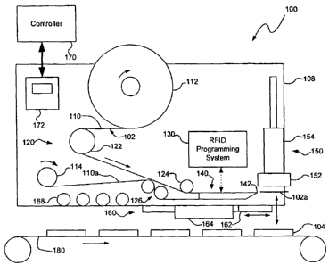
[0008] FIG. 1 is a diagrammatic view of a RFID applicator, consistent with one
embodiment of the invention.
[0009] FIG. 2 is a side cross-sectional view of one embodiment of a RFID label
that can
be used in the RFID applicator, consistent with one embodiment of the
invention.
[0010] FIG. 3 is a side view of one embodiment of a RFID applicator peeler
member
with an integrated RFID programming antenna.
[0011] FIGS. 4A-4C are side views of one embodiment of a label reject assembly
in
various positions with respect to a RFID applicator peeler member for use in a
RFID
applicator.
3
CA 02576316 2007-02-07
WO 2006/031423 PCT/US2005/030676
[0012] FIGS. 5A and 5B are side views of another embodiment of a label reject
assembly integrated into a RFID applicator peeler member for use in a RFID
applicator.
[0013] FIG. 6A is a side view of one embodiment of a label tamp assembly.
[0014] FIG. 6B is a top view of the label tamp assembly shown in FIG. 6A.
[0015] FIG. 7A is a bottom view of one embodiment of a vacuum tamp pad that
may be
used in a label tamp assembly.
[0016] FIG. 7B is a cross-section view of the vacuum tamp pad shown in FIG. 7A
taken
along line A-A.
[0017] FIG. 7C is a side view of the vacuum tamp pad shown in FIG. 7A.
[0018] FIG. 8A is a side view of another embodiment of a vacuum tamp pad for
use in a
RFID applicator.
[0019] FIG. 8B is a bottom view of the vacuum tamp pad shown in FIG. 8A.
Detailed Description
[0020] Numerous specific details may be set forth herein to provide a thorough
understanding of the embodiments of the disclosure. It will be understood by
those
skilled in the art, however, that various embodiments of the disclosure may be
practiced without these specific details. In other instances, well-known
methods,
procedures, components and circuits have not been described in detail so as
not to
obscure the various embodiments of the disclosure. It can be appreciated that
the
specific structural and functional details disclosed herein are representative
and do not
necessarily limit the scope of the disclosure.
4
CA 02576316 2007-02-07
WO 2006/031423 PCT/US2005/030676
[0021] It is worthy to note that any reference in the specification to "one
embodiment" or "an embodiment" according to the present disclosure means that
a
particular feature, structure, or characteristic described in connection with
the
embodiment is included in at least one embodiment. The appearances of the
phrase
"in one embodiment" in various places in the specification are not necessarily
all
referring to the same embodiment.
[0022] Referring to FIG. 1, radio frequency identification (RFID) label
applicator
100, consistent with embodiments of the invention, may be used to apply RFID
labels
102 to articles or items 104. The RFID label applicator 100 may also be used
to
program RFID labels 102, to detect defective RFID labels, and to reject the
defective
labels such that the defective labels are not applied to the items 104. The
articles or
items 104 may be products, merchandise, or any other items or articles that
may be
monitored using RFID techniques.
[0023] The RFID labels 102 may be removably secured to a backing material or
web
110 such that the RFID labels 102 are supported on the web 110 during
programming
and may be removed (e.g., peeled away from the web 110) for application. The
web
110 supporting the labels 102 may be rolled onto a roll 112, which is unwound
to
allow the web 110 to pass through the label applicator 100. After the RFID
labels 102
are removed or rejected, scrap web 110a may be rewound onto a rewind roll 114.
[0024] One embodiment of the RFID label applicator 100 may include a web
feeding
mechanism 120 to feed the web 110, a RFID programming system 130 to program
the
RFID labels 102, a peeler member 140 to peel the RFID labels 102 from the web
110,
a label tamp assembly 150 to apply the RFID labels 102 to the items 104, and a
label
CA 02576316 2007-02-07
WO 2006/031423 PCT/US2005/030676
reject assembly 160 to reject RFID labels. The RFID label applicator 100 may
also
include an applicator controller 170 to control operation of the RFID label
applicator
100. The articles or items 104 may be arranged in a line (e.g., a product
line) and may
be moved, for example, using a conveyor 180 or other similar mechanism.
Components in the applicator 100 may be mounted or secured to an applicator
frame
108.
[0025] The RFID label applicator 100 may also include other components not
shown
in FIG. 1. Examples of additional components include, but are not limited to,
a label
sensor to sense and position the labels 102 relative to the RFID programming
system
130, an item sensor to sense and position the items 104 relative to the tamp
assembly
150, and an integrated printer to print indicia on the labels 102. One example
of a
label sensor includes a thru-beam that shines a light from beneath the web to
a light
sensor 110 positioned above the web 110.
[0026] The web feeding mechanism 120 may include a tensioning roller 122 and
an
idler roller 124, which guide the web 110 with the RFID labels 102 to the
peeler
member 140. The web feeding mechanism 120 may also include a drive and nip
roller assembly 126 that takes up the scrap web I l0a and feeds the scrap web
110a to
the web rewind roll 114. The drive and nip roller assembly 126 may be driven
to pull
the scrap web I 10a, thereby causing the web 110 with the RFID labels 102 to
pass
around the peeler member 140. The unwind roll 112 and/or rewind roll 114 may
also
be driven (e.g., with servomotors) to facilitate unwinding of the web 110
and/or
rewinding the scrap web 110a.
6
CA 02576316 2007-02-07
WO 2006/031423 PCT/US2005/030676
[0027] The RFID programming system 130 may include a RFID reader/programmer
coupled to one or more RFID programming antennas, as will be described in
greater
detail below. The RFID programming system 130 may include any RFID
reader/programmer known to those skilled in the art for reading and/or
programming
RFID devices, such as the type known as the Sensormatic SensorIDTM Agile 2
Reader available from Tyco Fire and Security. The RFID programming system 130
may also be capable of detecting defective RFID labels, for example, by
attempting to
read a RFID label after applying programming signals.
[0028) The peeler member 140 may include a peel tip 142 having a radius and
forming an angle such that a RFID label 102 peels away from the web 110 as the
web
110 passes around the peel tip 142. In one embodiment, the radius of the peel
tip 142
may be in a range of about 0.030 in. and the angle formed by the peel tip 142
may be
in a range of about 90 or less. Other radii and angles are within the scope
of the
invention and may depend upon the adhesion properties (e.g., the adhesion
strength)
of the RFID labels 102 on the web 110. The peeler member 140 may be made of a
rigid material such as aluminum. In one embodiment, the peeler member 140 may
be
in the form of a plate or a bar, although those skilled in the art will
recognize other
shapes and configurations.
[0029] The label tamp assembly 150 may include a tamp pad 152 coupled to a
tamp
driving mechanism 154. The tamp pad 152 contacts the non-adhering side of a
RFID
label 102a that has been removed from the web 110 and holds the RFID label
102a.
The tamp driving mechanism 154 drives the tamp pad 152 and the RFID label 102a
toward the item 104 to which the RFID label 102a is to be applied. One
embodiment
7
CA 02576316 2007-02-07
WO 2006/031423 PCT/US2005/030676
of the tamp assembly 150 uses a vacuum pressure to retain the RFID label 102a
in
contact with the tamp pad 152. The vacuum pressure may be released and/or air
may
be blown from the tamp pad 152 to facilitate application of the RFID label
102a.
Although one embodiment of a label tamp assembly 150 is described herein, the
label
tamp assembly 150 may include any structure or mechanism for moving a label
into
contact with an item 104.
[0030] The label reject assembly 160 may include an accumulation pad 162
coupled
to a label reject driving mechanism 164. Upon determining that a RFID label
102 is
to be rejected, the reject driving mechanism 164 drives the accumulation pad
162 into
the path of the tamp pad 152. The tamp pad 152 then applies the rejected RFID
label
to the accumulation pad 162 instead of the item 104. A RFID label may be
rejected
when the label is determined to be defective or for other reasons. Although
one
embodiment of the label reject assembly 160 is described herein, the label
reject
assembly 160 may include any structure for intercepting or otherwise
preventing a
RFID label from being applied to an item 104.
[0031] The tamp driving mechanism 154 and the label reject driving mechanism
164
may include pneumatic actuated air cylinders, such as the type available from
PHD,
Inc. When air cylinders are used as the driving mechanisms, the RFID label
applicator 100 may also include one or more air pressure gauges 168 to monitor
and/or adjust operation of the air cylinders, as is known to those skilled in
the art.
Although the described embodiment uses air cylinders and rods, those skilled
in the
art will recognize that other linear actuators or driving mechanisms may be
used.
8
CA 02576316 2007-02-07
WO 2006/031423 PCT/US2005/030676
[0032] The applicator controller 170 may be a programmable logic controller
(PLC),
such as the type available from Allen-Bradley, Omron or Mitsubishi or a
general
purpose computer, such as a PC, programmed to control one or more operations
of the
applicator 100. The controller 170 may be coupled to the web feeding mechanism
120 (e.g., to the motors, sensors, etc.) to control the feeding of the web 110
around the
peeler member 140 and/or to control the positioning of the RFID labels 102
relative to
the RFID programming system 130. The controller 170 may also be coupled to the
tamp assembly 150 to control application (or tamping) of programmed and
removed
RFID labels to the items 104. The controller 170 may also be coupled to the
label
reject assembly 160 to control the rejection of labels, for example, when the
label is
determined to be defective. The controller 170 may also be coupled to a user
interface / control panel 172 to enable a user to monitor the application
process and/or
to provide commands and/or operating parameters to the controller 170.
[0033] The controller 170 and/or user interface 172 may also be coupled to the
RFID
programming system 130 to control the RFID programming operations. RFID
programming operations may be controlled, for example, by allocating
Electronic
Product Codes (EPC's) and/or other data to be sent to the RFID labels 102 upon
receiving an indication that the RFID labels 102 are properly positioned
relative to the
RFID programming system 130. The controller 170 may also monitor the detection
of defective labels to control the label reject assembly 160. The controller
170 may
further collect programming data and statistics and provide such data to the
user.
[0034] According to one method of operation, the web 110 may be advanced
around
the peeler member 140, for example, by using the drive and nip roller assembly
126 to
9
CA 02576316 2007-02-07
WO 2006/031423 PCT/US2005/030676
pull the web 110. As the web 110 is advanced, the unwind roll 112 unwinds the
web
110 supporting the RFID labels 102 and the rewind roll 114 rewinds the scrap
web
110a after the RFID labels 102 have been applied or rejected. When each RFID
label
102 on the web 110 is positioned within a programming range of the RFID
programming system 130, the RFID programming system 130 may program the RFID
label 102 by transmitting radio frequency (RF) programming signals to the RFID
label 102 and attempting to read the RFID label 102. The RFID label 102 may
then
be advanced around the peel tip 142 of the peeler member 140 to remove the
RFID
label 102. A removed RFID label 102a may then be applied to an item 104 using
the
tamp assembly 150 or may be rejected using the label reject assembly 160.
These
operations may be repeated for each of the RFID labels 102 on the web 110 and
the
items 104 may be advanced such that programmed RFID labels 102 are applied to
each of the items 104.
[0035] One embodiment of a RFID label 102 is shown in greater detail in FIG.
2.
The RFID label 102 may include an integrated circuit (IC) chip 202 coupled to
an
antenna 204. The IC chip 202 and antenna 204 may be sandwiched between one or
more layers or substrates, such as an adhesive substrate 206 and a printable
layer 208.
The adhesive substrate 206 may include a scrim coated on each side with an
adhesive,
such as an acrylic based adhesive. The printable layer 208 may be made of a
thermal
transfer paper or other material suitable for printing. One or more additional
layers or
substrates may also be incorporated into the RFID label 102, as is known to
those
skilled in the art. The web 110 may be made of a paper with a release agent
such as
wax or silicone to allow the RFID label 102 to peel away from the web 110. The
CA 02576316 2007-02-07
WO 2006/031423 PCT/US2005/030676
RFID label 102 may have a peel adhesion strength (e.g., about 15 N/inch) that
allows
the RFID label 102 to be removably adhered to the web 110 and later adhered to
the
items 104. Although RFID labels may have various sizes, one example of the
RFID
label 102 may be about 3 in. by 3 in. and supported on a web 110 having a
width of
about 4 in.
[0036] One example of a RFID label 102 is the "Combo EAS/RFID Label or Tag"
disclosed in U.S. Provisional Patent Application Serial No. 60/628,303, which
is fully
incorporated herein by reference. Other examples include the RFID labels
commercially available under the name Sensormatic from Tyco Fire and
Security.
Those skilled in the art will recognize that the RFID label 102 may include
any RFID
device capable of being adhered or otherwise secured to articles or items.
[0037] Referring to FIG. 3, one embodiment of a peeler member 140a is
described in
greater detail. The peeler member 140a may include a RFID programming antenna
132 integrated with the peeler member 140 and connected to a RFID
reader/programmer 134. Each RFID label 102 may thus be programmed and verified
just before peeling the label and transferring the label to the tamp pad 152
(see FIG.
1). The proximity of the RFID programming antenna 132 to the peel tip 142
allows
each defective RFID label to be handled immediately (i.e., without having to
track
defective labels from a point of detection to a point of application further
downstream), which may ensure that defective labels are subject to rejection
and
programmed labels are applied to items.
[0038] According to one embodiment, the RFID programming antenna 132 may be a
near-field probe such as the type disclosed in U.S. Provisional Patent
Application
11
CA 02576316 2007-02-07
WO 2006/031423 PCT/US2005/030676
Serial No. 60/624,402, which is fully incorporated herein by reference. The
programming range of a near-field probe is generally the near-field zone of
the
antenna or probe. The near field probe may be implemented by enhancing the
magnitude of the induction field within the near-near field zone associated
with an
antenna structure and decreasing the magnitude of the radiation field within
the far-
field zone associated with the antenna structure. One embodiment of the near
field
probe may include a stripline antenna terminated into a 50 ohm chip resistor.
In one
example, the near field probe may have an operating frequency of 915 MHz and
the
near-field zone may be approximately 5 cm from the probe. One example of the
probe may be about 2 to 3 in. long, although those skilled in the art will
recognize that
smaller probes may be used to allow programming of labels that are smaller
and/or
spaced closer together on the web.
[0039] This embodiment of the peeler member 140a may include a cavity 302 in a
body portion 304 of the peeler member 140a, which is configured to receive the
RFID
programming antenna 132. A cover 306 may be used to cover the cavity 302. The
cover 306 may be made of, or at least coated with, a non-reflective material
that will
not reflect or absorb the radio frequency waves transmitted by the RFID
programming
antenna 132 and the RFID device antenna 204. For example, the cover 306 may be
made of a plastic material such as the type available under the name DelrinTM.
A
cable 308 may connect the RFID programming antenna 132 to the RFID
reader/programmer 134. The cable 308 may extend from the RFID programming
antenna 132 through one side 310 of the body portion 304 of the peeler member
140a.
12
CA 02576316 2007-02-07
WO 2006/031423 PCT/US2005/030676
[0040] The RFID programming antenna 132 may be positioned within the cavity
302
such that the RFID programming antenna 132 transmits radio frequency (RF)
programming signals to a RFID label 102b positioned over the RFID programming
antenna 132 (i.e., within the programming range). The cavity 302 may include
an
adjustment region 312 that allows the RFID programming antenna 132 to be
adjusted
laterally within the cavity 302 to accommodate different sizes of labels. For
example,
the RFID programming antenna 132 may be configured initially to align with the
IC
in labels having a certain size (e.g., 3 in. by 3 in.) and may need to be
adjusted
laterally for labels that are smaller or larger. In one example, the lateral
adjustment of
a probe having a length of about 2 to 3 in. may be in a range of about 1 to
1.5 inches
in either direction. An adjustment mechanism, such as a bar or rod 320, may be
coupled to the RFID programming antenna 132 to provide mechanical adjustment.
[0041] Although the described embodiment shows the RFID programming antenna
132 located inside of the cavity 302 in the peeler member 140a, the RFID
programming antenna 132 may also be integrated with the peeler member 140a in
other ways. For example, the RFID programming antenna 132 may be mounted
anywhere such that an RFID label 102b on the peeler member 140a is within the
programming range (e.g., the near field) of the programming antenna 132.
[0042] According to one method of programming RFID labels, the web 110 may be
advanced along the peeler member 140a until a RFID label 102b is positioned
within
a programming range of the RFID programming antenna 132. The RFID label 102b
may be positioned, for example, by stopping advancement of the web 110 when a
label sensor (not shown) senses an edge of the RFID label 102b. When
positioned,
13
CA 02576316 2007-02-07
WO 2006/031423 PCT/US2005/030676
RF programming signals may be transmitted to the RFID label 102b from the RFID
programming antenna 132. RF signals may also be transmitted from the RFID
label
102b to the RFID programming antenna 132 in an attempt to read and validate
the
RFID label 102b. If the RFID label 102b cannot be read or validated, the RFID
reader/programmer 134 may indicate that the RFID label 102b is defective.
After the
RFID label 102b is either programmed or determined to be defective, the web
110 is
advanced along the peeler member 140a until the next RFID label 102 is located
in
the programming range of the RFID programming antenna 132.
[0043] A programmed RFID label 102a may be subsequently removed as the web 110
supporting the programmed RFID label 102a passes around the peel tip 142. In
this
described embodiment, the programmed RFID label 102a is removed when the next
RFID label 102b is positioned in the programming range. The next RFID label
102b
may be programmed after the programmed RFID label 102a is applied to an item
or
may be programmed while the programmed RFID label 102a is applied to an item.
[0044] Referring to FIGS. 4A-4C, one embodiment of the label reject assembly
160 is
described in greater detail. The accumulation pad 162 may include at least a
substrate
that is sufficiently rigid to receive and adhere to a rejected RFID label
applied by the
tamp pad 152. The reject driving mechanism 164 may be mounted in any location
that enables the accumulation pad 162 to be driven into a path 400 of the tamp
apply
stroke (i.e., between the tamp pad 152 and the item 104) and then withdrawn
such that
the tamp pad 152 will clear the accumulation pad 162 and the rejected label(s)
on the
accumulation pad 162.
14
CA 02576316 2007-02-07
WO 2006/031423 PCT/US2005/030676
100451 The accumulation pad 162 may be configured to receive multiple rejected
RFID labels stacked on previous rejected labels. The accumulation pad 162 may
also
be configured to receive rejected labels adjacent to other rejected labels
(e.g., multiple
adjacent stacks). The accumulation pad 162 may be sized according to the size
of the
labels and the manner in which the labels are accumulated (e.g., one stack or
adjacent
stacks) on the accumulation pad. For example, an accumulation pad 162 may have
a
size that is capable of adhering to and receiving at least one label or may
have a size
that is capable of receiving multiple adjacent stacks of labels.
[0046] The accumulation pad 162 may include a low surface energy medium, such
as
polytetrafluoroethylene, at least on the surface of the accumulation pad 162,
which
allows the accumulated RFID label(s) to be easily removed by peeling away the.
bottom label. The accumulation pad 162 may also include a removable layer,
such as
an index card material, to allow the accumulated RFID label(s) to be removed.
[00471 According to one method of rejecting RFID labels, the RFID labels 102
on the
web 110 may. be programmed prior to passing the web 110 around the peel tip
142 of
the peeler member 140, for example, as described above. Programming the RFID
labels may include detecting any defective RFID labels that should be
rejected. A
RFID label 102a that is properly programmed may be removed and applied to an
item
(FIGS. 4A and 4B). Upon detecting a defective RFID label 102c, the label
accumulation pad 162 may be extended from a retracted position (FIGS. 4A and
4B)
to an extended position (FIG. 4C) into the path 400 between the tamp pad 152
and the
item 104. In the extended position, the label accumulation pad 162 prevents a
full
tamp apply stroke down to the item 104 and thus intercepts the rejected RFID
label
CA 02576316 2007-02-07
WO 2006/031423 PCT/US2005/030676
102c before the rejected RFID label 102c is applied to an item 104. The tamp
pad
152 may apply the rejected RFID label 102c to the accumulation pad 162 in the
same
manner as applying labels to items 104, as described in greater detail below.
The
accumulation pad 162 with the rejected RFID label(s) 102c applied thereto may
then
be retracted and normal label application may continue.
[0048] The accumulation pad 162 may also be extended to different positions
within
the path 400 of the tamp apply stroke such that labels are received on the
accumulation pad 162 adjacent to other labels. The controller 170 may control
the
reject driving mechanism 164 to control positioning of the accumulation pad
162 such
that labels are positioned in an organized fashion (e.g., spread evenly) on
the
accumulation pad 162.
[0049] The accumulated rejected RFID labels may be removed from the
accumulation
pad 162 after a number of rejected labels accumulate on the accumulation pad
162.
The number of accumulated rejected labels may be monitored. According to one
method, a numeric reject number may be printed (e.g., using an integrated
printer) on
the surface of a rejected label 102c and a reject label counter (e.g., in the
controller
170) may be incremented. The controller 170 may provide an indication to the
user as
to when the accumulated labels should be removed. When the stack of
accumulated
labels is removed, the last numeric reject number on the top accumulated label
will
signify the sum of the accumulated labels in the stack, for customer recording
purposes.
[0050] In one embodiment, about twenty (20) to thirty (30) labels may be
accumulated on the accumulation pad 162 before removing the labels. One
16
CA 02576316 2007-02-07
WO 2006/031423 PCT/US2005/030676
embodiment of the RFID label applicator 100 may have a label programming
failure
rate of about 5%. In other words, about 5 out of every 100 RFID labels may be
rejected as defective, which allows about 400 to 600 RFID labels to be applied
before
the stack of accumulated labels is removed. The label reject assembly 160 thus
allows labels, such as defective RFID labels, to be rejected (i.e., not
applied to an item
104) with minimal or no interruption to the label application process.
Alternatively, a
rejected RFID label may be removed from the accumulation pad 162 after each
rejected label is intercepted by the accumulation pad 162.
[0051] An alternative embodiment of a label reject assembly may include the
extendable path altering mechanism 500 shown in FIGS. 5A and 5B. The
extendable
path altering mechanism 500 is extendable from a retracted position (FIG. 5A)
to an
extended position (FIG. 5B). In the extended position, the extendable path
altering
mechanism 500 may alter a path of the web 110 around the peel tip 142,
effectively
enlarging the radius of the peel tip 142. As a result, a rejected RFID label
102d
passing around the peel tip 142 does not peel away from the web 110 and
continues
moving with the scrap web 110a instead of being applied to an item. Rejected
RFID
labels, such as defective RFID labels, may thus be handled automatically with
minimal or no effect on the application process.
[0052] The extendable path altering mechanism 500 may include an extendable
tip
502 coupled to a tip driving mechanism 504. The extendable tip 502 may be
rounded
with a larger radius than the peel tip 142. In one example, the radius of the
extendable tip 502 may be in a range of about 0.25 to 0.5 in. The extendable
tip 502
may be made of plastic, aluminum or other suitable material that allows the
web 110
17
CA 02576316 2007-02-07
WO 2006/031423 PCT/US2005/030676
to slide around the extendable tip 502. The tip driving mechanism 504 may
include a
pneumatic actuated air cylinder, although those skilled in the art will
iecognize that
other linear actuators or driving mechanisms may be used.
[0053] In one embodiment, the extendable path altering mechanism 500 may be
integrated with another embodiment of the peeler member 140b. The peeler
member
140b may include a cavity 510 for receiving the extendable path altering
mechanism
500. Alternatively, the extendable path altering mechanism 500 may be located
adjacent to the peeler member 140b as long as the extendable tip 502 can
extend to
alter the path of the web 110 in a manner that will prevent a label from
peeling away.
The peeler member 140b may also include the RFID programming antenna 132
integrated with the peeler member 140b, for example, as described above.
[0054] According to one method of rejecting RFID labels using the extendable
path
altering mechanism 500, a RFID label 102b on the web 110 may be programmed
prior to passing the RFID label around the peel tip 142 of the peeler member
140b, for
example, using the integrated RFID programming antenna 132. Programming the
RFID label 102b may include detecting whether or not the RFID label 102b is
defective, e.g., by attempting to read information programmed thereon. A RFID
label
102a that is properly programmed is caused to peel away from the web 110 as
the web
110 and the RFID label 102a passes around the peel tip 142 of the peeler
member
140b. Upon detecting a defective RFID label 102d, the path of the web 110
around
the peel tip 142 may be altered using the extendable path altering mechanism
500, for
example, by extending the extendable tip 502 beyond the peeler tip 142. When
the
extendable tip 502 is extended, the web 110 may be advanced to position the
next
18
CA 02576316 2007-02-07
WO 2006/031423 PCT/US2005/030676
RFID label 102 for programming and/or application and the rejected RFID label
102d
passes around the extendable tip 502 and remains on the scrap web 110a instead
of
being applied to the tamp pad 152. The extendable tip 502 may then be
retracted and
normal label application may continue.
[0055] To allow the path of the web 110 to be altered, the tension in the web
110 may
be released such that the scrap web 110a unwinds and the position of the RFID
label
102b can be maintained on the peeler member 140b. The tension in the web 110
may
be released, for example, by releasing a torque brake on a motor driving the
web
rewind roll and/or releasing the drive and nip roller assembly.
[0056] Referring to FIGS. 6A and 6B, another embodiment of the tamp assembly
150a is described in greater detail. The tamp assembly 150a may include a
vacuum
tamp pad 600 coupled to an air manifold 602. The vacuum pad 600 may include
one
or more vacuum holes 610 extending through the vacuum pad 600 to a label
contacting side 612. The manifold 602 may include an inlet/outlet 620 and at
least
one air chamber 622 located over the vacuum holes 610 in the vacuum pad 600.
The
inlet/outlet 620 may be coupled to an,air supply or compressor, which may be
switched between compressed air and a vacuum. When a vacuum is applied, air
may
be drawn through the inlet/outlet 620 and the chamber 622 in the manifold 602,
which
causes air to be drawn through the vacuum holes 610 in the vacuum pad 600. As
a
result, a vacuum pressure is generated around the vacuum holes 602 on the
label
contacting side 612 of the vacuum pad 600, which is sufficient to hold the
label 102
against the vacuum pad 600.
19
CA 02576316 2007-02-07
WO 2006/031423 PCT/US2005/030676
[0057] As shown in FIG.S 7A-7C, the vacuum tamp pad 600 may include slots or
channels 614 extending along the label contacting side 612 to promote air
discharge
when the vacuum is drawn. The slots or channels 614 may also provide for less
friction against a label when transferring the label to the tamp pad 600
(e.g., in the
label feed direction 604). The vacuum tamp pad 600 may also include a relief
area
616 configured to receive the portion of the RFID label with the IC chip. The
relief
area 616 protects the IC chip from stresses due to abrasion during label
transfer to the
pad 600 and protects the IC chip from compressive stresses during tamp
placement of
the RFID label onto an item or product. The vacuum tamp pad 600 may further
include a chamfer 618 at a leading edge 617 of the vacuum tamp pad 600 to
promote
easy label transfer to the tamp pad 600, as the label moves in the label feed
direction
604 from the peeler member.
[0058] The embodiment of the vacuum tamp pad 600 shown in FIG.S 7A-7C is
designed for a 3 in. x 3 in. RFID label. For this example, the vacuum pad 600
may
have a length 1 of about 3.125 in., a width w of about 3.00 in. and a
thickness t of
about 0.25 in. The tamp pad 600 may be made of a plastic material, such as the
type
available under the name Delrin, or other suitable materials.
[0059] This described embodiment of the vacuum pad 600 includes four (4)
vacuum
holes 610a-610d. The vacuum holes 610a-610d may be located to minimize the
effect
of label bow or curl and to allow each of the vacuum holes 610a-610d to be
sealed
regardless of the amount of label bow, thereby effectively holding the label
on the
vacuum pad 600. For example, the holes 610a and 610c may be located in from
the
leading edge 617 about'/4 of the length of the vacuum pad 600 and the holes
610b and
CA 02576316 2007-02-07
WO 2006/031423 PCT/US2005/030676
610d may be located in from the leading edge 617 about 3/4 of the length of
the
vacuum pad 600. The holes 610a and 610b may be located in from the side edge
619
about 1/3 of the length of the vacuum pad 600 and the holes 610c and 610d may
be
located in from the side edge 619 about 2/3 of the length of the pad 600. The
holes
610a-610d may have a diameter of about 0.093".
[0060] The vacuum pad 600 and/or manifold 602 may be mounted to a mounting
block 630 with one or more compression springs 632 positioned therebetween
(FIG.
6A). The compression springs 632 may compress as needed when the vacuum tamp
pad 600 contacts a product, allowing the tamp pad 600 to mate parallel with a
surface
of an item or product to which a label is being applied. The mounting block
630 may
include tapered holes 634 that receive shoulder bolts 636, which secure the
compression springs 632 and allow the compression springs 632 to compress.
Although the described embodiment shows four (4) compression springs 632, any
number of compression springs may be used to provide the desired compression,
as
may be determined by one of ordinary skill in the art.
[0061] A proximity sensor 640 may also be mounted to the manifold 602 or to
the
vacuum tamp pad 600 to detect the surface of the item or product to which the
label is
to be applied. The proximity sensor 640 may thus enable consistent compression
of
the compression springs 632 when labels are being applied to items or products
having surfaces at different levels.
[0062] The tamp assembly 150 may also include a cylinder 650, such as a
pneumatic
actuated air cylinder, and rod 652 for providing the linear driving force. A
cylinder
mounting block 654 may be used to mount the mounting block 630 to the rod 652.
21
CA 02576316 2007-02-07
WO 2006/031423 PCT/US2005/030676
Those skilled in the art will recognize that other linear actuators or driving
mechanisms may also be used.
[0063] According to an alternative embodiment, shown in FIGS. 8A and 8B, a
vacuum tamp pad 800 may include only three vacuum holes 810a-810c. A manifold
802 with an inlet/outlet 820 may be coupled to the tamp pad 800 to cause air
to pass
through the vacuum holes 810a-810c. The vacuum holes 810a-810c may be
positioned such that the leading portion of a RFID label 102 is secured by the
vacuum
force when the RFID label 102 is properly positioned. The trailing portion of
the
RFID label 102 may be left free (i.e., not subject to a vacuum) to relieve bow
in the
label 102. The vacuum hole 810c near the far edge of the RFID label 102 may
act as
a label stop. The vacuum holes 810a-810c thus take into account the natural
bow that
is inherent to RFID labels that are provided in roll format.
[0064] A fixed stop 808 may be positioned adjacent the vacuum pad 800 to allow
the
label to feed (i.e., in the feed direction 804) and orient properly. When the
RFID label
102 is being fed to the side of an item (e.g., a box) at a 90 degree angle
relative to a
vertical plane (i.e., sideways), the fixed stop 808 may prevent a gravity
force 806
from misaligning the RFID label 102 with respect to the vacuum pad 800. The
fixed
stop 808 may be fixed (e.g., bolted) to a bottom side of the tamp 'driving
mechanism
or cylinder.
[0065] The vacuum holes 810a-810c may also be positioned to hold the RFID
label
102 in place without subjecting the IC chip 202 in the RFID label 102 to
vacuum
forces at the holes 810a-810c. The vacuum pad 800 may also be recessed (not
shown)
in the area receiving the IC chip 202 to provide additional relief. The vacuum
pad
22
CA 02576316 2007-02-07
WO 2006/031423 PCT/US2005/030676
800 may also include a compressible material, to avoid damage to the IC chip
202 in
the RFID label 102.
[0066] While the principles of the invention have been described herein, it is
to be
understood by those skilled in the art that this description is made only by
way of
example and not as a limitation as to the scope of the invention. Other
embodiments are
contemplated within the scope of the invention in addition to the embodiments
shown
and described herein. Modifications and substitutions by one of ordinary skill
in the art
are considered to be within the scope of the invention, which is not to be
limited except
by the following claims.
23