Note: Descriptions are shown in the official language in which they were submitted.
CA 02576512 2007-02-06
WO 2006/017606 PCT/US2005/027634
METHOD AND APPARATUS FOR CONTROLLING TRANSMIT
POWER IN A WIRELESS COMMUNICATIONS DEVICE
Claim of Priority under 35 U.S.C. 119
[0001] The present Application for Patent claims priority to Provisional
Application
No. 60/599,390 entitled "Method for Clipping peak Transmit Power while
Limiting
Out-of-Band Emissions in a Wireless Communications System" filed August 6,
2004,
and assigned to the assignee hereof and hereby expressly incorporated by
reference
herein.
BACKGROUND
Field
[0002] The present disclosure relates generally to wireless communications,
and more
particular, to systems and methods for controlling the transmit power in a
wireless
communications device.
[0003] Wireless communication systems are designed to allow multiple users to
share a
common communications medium. Numerous multiple-access techniques are known in
the art such as Code Division Multiple Access (CDMA), time division multiple
access,
frequency division multiple access, as well as many other similar multi-access
techniques. The multi-access concept is based on channel allocations that
separate
communications among multiple users. By way of example, in CDMA communication
systems, channel separation may be achieved by transmitting each signal with a
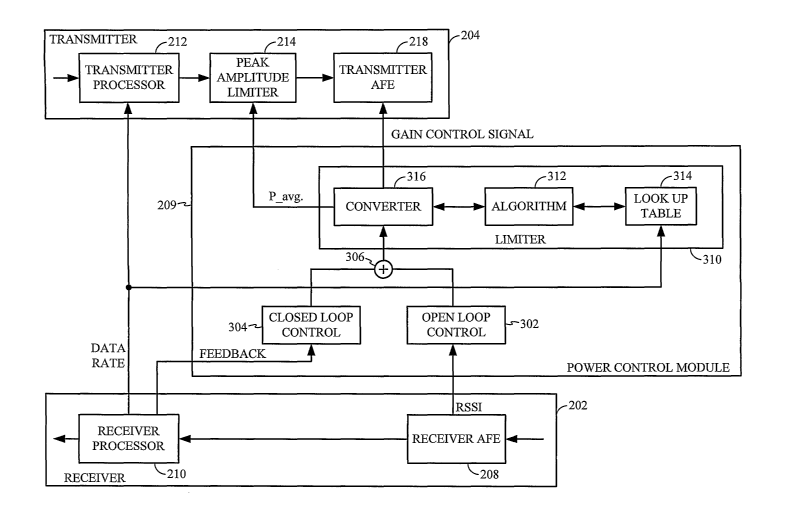
different code that modulates a carrier, and thereby, spreads the signal over
the entire
frequency spectrum. The transmitted signals can be separated in the receiver
by a
demodulator using a corresponding code to de-spread the desired signal. The
undesired
signals, whose codes do not match, contribute only to noise.
[0004] The ability of a receiver to separate the transmitted signal from the
noise may be
measured by the Signal-to-Noise Ratio (SNR). The average signal transmission
power
may be controlled at the transmitter to achieve a specific SNR at the receiver
in
accordance with the quality of service requirements. Typically, a higher SNR
is
required to achieve a higher data rate that might be required for a video or
other high
CA 02576512 2007-02-06
WO 2006/017606 PCT/US2005/027634
2
bandwidth transmission. A higher SNR may also be required if the transmitter
is far
away from the receiver. In either case, improvements in the SNR may be
achieved by
increasing the average signal transmit power at the transmitter.
Unfortunately, this
increase may result in signal power peaks that exceed regulatory limits, such
as those
imposed by the Federal Communications Commission in the United States. This
may
occur in CDMA communication systems where each user simultaneously transmits
over
the same frequency spectrum. Multilevel modulation and transmit pulse shape
filtering
further increase the probability that the peak transmit power may exceed the
regulatory
limits.
[0005] One way to increase the average transmit power while maintaining the
peak
transmit within the regulatory limits is to clip the signal when the
instantaneous transmit
power is above a certain threshold. However, clipping a signal can
significantly
increase the out-of band emissions, as well as introduce distortion in the
signal. Out-of-
band emissions are also regulated, and therefore, may significantly limit the
use of
clipping to reduce peaks in the signal power.
[0006] Accordingly, there is a need in the art for optimizing the average
transmit power
to maintain a desired quality of service, and still meet the regulatory limits
for both peak
transmit power and out-of-band emissions.
SUMMARY
[0007] In one aspect of the present invention, a method of wireless
communications
includes generating a signal, setting an average transmit power of the signal
transmission as a function of a first threshold relating to out-of-band
emissions, clipping
the signal as a function of a first threshold relating to peak transmit power,
and
transmitting the signal over a wireless medium.
[0008] In another aspect of the present invention, a wireless communications
device
includes a user interface configured to generate a signal, a power control
module
configured to set an average transmit power of the transmitter as a function
of a first
threshold relating to out-of-band emissions, a peak amplitude limiter
configured to clip
the signal as a function of a second threshold relating to peak transmit
power, and a
transmitter configured to transmit the signal over a wireless medium.
[0009] In yet another aspect of the present invention, a wireless
communications device
includes means for generating a signal, means for setting an average transmit
power of
the signal transmission as a function of a first threshold relating to out-of-
band
CA 02576512 2007-02-06
WO 2006/017606 PCT/US2005/027634
3
emissions resulting from the clipping of the signal, means for clipping the
signal as a
function of a second threshold relating to peak transmit power, and means for
transmitting the signal over a wireless medium.
[0010] It is understood that other embodiments of the present invention will
become
readily apparent to those skilled in the art from the following detailed
description,
wherein various embodiments of the invention are shown and described by way of
illustration. As will be realized, the invention is capable of other and
different
embodiments and its several details are capable of modification in various
other
respects, all without departing from the spirit and scope of the present
invention.
Accordingly, the drawings and detailed description are to be regarded as
illustrative in
nature and not as restrictive.
BRIEF DESCRIPTION OF DRAWINGS
[0011] FIG. 1 is a conceptual block diagram illustrating an example of a
variable data
rate CDMA communications system;
[0012] FIG. 2 is a functional block diagram illustrating an example of a
subscriber
station for use in a variable data rate CDMA communications system;
[0013] FIG. 3 is a functional block diagram illustrating an example of a power
control
module for use in a subscriber station operating in a variable data rate CDMA
communications system;
[0014] FIG. 4 is a functional block diagram illustrating one embodiment of a
peak
amplitude limiter for use in a subscriber station operating in a variable data
rate CDMA
communications system; and
[0015] FIG. 5 is functional block diagram illustrating another embodiment of a
peak
amplitude limiter for use in a subscriber station operating in a variable data
rate CDMA
communications system.
DETAILED DESCRIPTION
[0016] The detailed description set forth below in connection with the
appended
drawings is intended as a description of various embodiments of the present
invention
and is not intended to represent the only embodiments in which the present
invention
may be practiced. The detailed description includes specific details for the
purpose of
providing a thorough understanding of the present invention. However, it will
be
apparent to those skilled in the art that the present invention may be
practiced without
CA 02576512 2007-02-06
WO 2006/017606 PCT/US2005/027634
4
these specific details. In some instances, well-known structures and
components are
shown in block diagram form in order to avoid obscuring the concepts of the
present
invention.
[0017] In the following detailed description, various power control techniques
may be
described in the context of a CDMA wireless communications device. While these
power control techniques may be well suited for use in this application, those
skilled in
the art will readily appreciate that these inventive aspects are likewise
applicable in
various other communication and/or electronic devices. Accordingly, any
reference to a
CDMA wireless communications device is intended only to illustrate the
inventive
aspects, with the understanding that such inventive aspects have a wide range
of
applications.
[0018] FIG. 1 is a conceptual block diagram illustrating an example of a CDMA
communications system employing a variable data rate request scheme. The CDMA
communications system may include a wireless network 102 having a base station
controller (BSC) 104. The BSC 104 may be used to interface the wireless
network 102
to a communications network 105. The communications network 105 may be a
packet-
based network, such as the Internet, a corporate intranet, or the like.
Alternatively, the
communications network 105 may be a circuit-switched network, such as, a
public
switched telephone network (PSTN). The wireless network 102 may be implemented
with any number of base stations dispersed throughout a geographic region. The
geographic region may be subdivided into smaller regions known as cells with a
base
station serving each cell. For simplicity, one base station 106 is shown
serving an entire
sector under control of the BSC 104. Three subscriber stations 108a-c are
shown in
communication with the base station 106. Each subscriber station 108a-c may
access
the communications network 105, or communicate with other subscriber stations,
through one or more base stations.
[0019] In the illustrative CDMA communications system, the forward and reverse
link
data rates may be controlled to optimize system capacity by means well known
in the
art. The "forward link" refers to transmissions from the base station 106 to a
subscriber
station 108, and the "reverse link" refers to transmissions from a subscriber
station 108
to the base station 106. For the purposes of illustration, the various
inventive concepts
will be described with reference to the reverse link, with the understanding
that such
inventive concepts are equally applicable to the forward link as well.
CA 02576512 2007-02-06
WO 2006/017606 PCT/US2005/027634
[0020] In the reverse link, the base station 106 may determine the data rate
for reverse
link communications with each subscriber station in its cell. The data rate
selected by
the base station 106 may be based on the type of communications supported, or
any
other criteria. By way of example, the base station may determine that a high
data rate
is required for communications encompassing a video application. Conversely,
the base
station 106 may select a lower data rate for voice communications. Other
factors may
also weigh in on the decision by the base station to assign a particular data
rate to the
subscriber station 108. By way of example, a fairness criteria that considers
the amount
of information to be transmitted by the subscriber station 108 and the delay
already
experienced by the subscriber station 108 may be considered. In any event, the
data rate
selected by the base station 106 may be embedded in the forward link
transmission to
the subscriber station 108.
[0021] A power control system may be employed to reduce mutual interference
between multiple subscriber stations operating in the same cell. The average
reverse
link transmission power is typically controlled by two power control loops.
The first
power control loop is an open loop control. The open loop control is designed
to
control the average reverse link transmission power as a function of the path
loss, the
effect of the base station loading, and environmentally induced phenomena
such, as fast
fading and shadowing. The second power control loop is a closed loop control.
The
closed loop control has the function of correcting the open loop control to
achieve a
desired SNR and frame error rate (FER) at the base station. This may be
achieved by
measuring the average power of the reverse link transmission at the base
station 106 and
providing feedback to the subscriber station 108 to adjust the average
transmit power of
the reverse link. Both the open and closed loop controls are well known in
CDMA
communication systems.
[0022] In the illustrative embodiment of the CDMA communications system
described
thus far, the reverse link peak transmit power measured over some period of
time may
be significantly above the average power measured over a longer period of
time. The
relation between the two may be defined by a Peak-to-Average Ratio (PAR). If
the
power control system is used to limit the peak transmit power in accordance
with the
regulatory limits, or any other system requirement, a critical PAR may be
determined
that defines the maximum average transmit power to meet the out-of-band
emission
requirements. By way of example, if the system requirements impose a peak
transmit
CA 02576512 2007-02-06
WO 2006/017606 PCT/US2005/027634
6
power of 20 Watts (W), and a critical PAR for the subscriber station is
determined to be
times above the average transmit power, then the average transmit power would
need
to be limited to 2 W to meet the out-of-band emission requirements. If the
average
transmit power were to exceed 2 W, the out-of-band emission requirements may
not be
met.
[0023] The critical PAR may be determined based on the system requirements on
peak
transmit power and out-of-band emissions, and on one or more parameters
relating to
the processing of the signal. The one or more parameters may include the
transmit filter
characteristics, the signal data rate, and/or the modulation scheme. The
critical PAR
may be determined through an off-line calibration procedure. The calibration
procedure
may be performed in a variety of ways. By way of example, a limiter may be
used to
clip the signal when it exceeds the peak power while the average transmit
power may be
increased slowly from a minimum value to a maximum value. The average transmit
power may be controlled by simulating feedback from a base station for the
power
control loop. During the calibration procedure, the out-of-band emissions may
be
monitored with any standard test equipment. The average transmit power that
causes
the out-of-band emissions to reach the limit imposed by the system
requirements is
recorded. The critical PAR may then be computed from the system requirements
on
peak transmit power and the average transmit power recorded during the
calibration
procedure. In a manner to be described in greater detail later, the critical
PAR may be
stored in the subscriber station and used during operation to limit the
average transmit
power.
[0024] In CDMA communication systems with variable transmission formats, a
critical
PAR may be computed for each transmission format during the calibration
procedure.
Each transmission format may include a data rate, a modulation scheme, an
encoding
scheme and a payload size. In one embodiment of the CDMA communications
system,
each transmission format can be identified by its data rate, with each data
rate having a
fixed encoding and modulation scheme, as well as a fixed payload size. In this
embodiment, the results of the calibration procedure can be recorded as shown
below in
Table 1.
CA 02576512 2007-02-06
WO 2006/017606 PCT/US2005/027634
7
TABLE 1
Data rate Critical PAR
(kb s (dB)
0 8.55
19.2 6.88
38.4 6.03
76.8 5.17
115.2 4.81
153.6 4.55
230.4 4.43
307.2 4.34
460.8 5.63
614.4 5.48
921.6 6.53
1228.8 6.36
Table 1 shows the critical PAR at each data rate. This table may be stored in
the
subscriber station 108 and used during operation to limit the average transmit
power of
the subscriber station. This allows a different average transmit power level
for each
data rate such that the highest possible average transmit power can always be
used.
[0025] FIG. 2 is a functional block diagram illustrating an example of a
subscriber
station for use in a variable data rate CDMA communications system. The
subscriber
station 108 may include a receiver 202 and transmitter 204 coupled to an
antenna 206.
A power control module 209 may be used to control both the peak and average
power of
the transmitter 204.
[0026] The receiver 202 may include a receiver analog front end (AFE) 208 and
a
receiver processor 210. The receiver AFE 208 may be used to amplify, filter
and
downconvert the radio frequency (RF) signal received from the antenna 206 to a
digital
baseband signal. The receiver AFE 208 may also provide a receiver signal
strength
indicator (RSSI) signal to the power control module 209 to compute the path
loss
between the base station and the subscriber station for open loop control
computations.
[0027] The digital baseband signal generated by the receiver AFE 208 may be
provided
to the receiver processor 210. The receiver processor 210 may be used to
convert the
digital baseband signal to information needed to drive various user interfaces
211, such
as a display, ringer, vibrator, audio speaker, and/or the like. The conversion
of the
CA 02576512 2007-02-06
WO 2006/017606 PCT/US2005/027634
8
digital baseband signal to this type of information may include various signal
processing
functions including demodulation, forward error correction, and spread
spectrum
processing.
[0028] The digital baseband signal may also include a number of control
signals. One
such control signal is the feedback from the base station indicating whether
to increase
or decrease the average transmit power of reverse link at the base station.
This feedback
may be extracted by the receiver processor 210 and provided to the power
control
module 209 for closed loop control computations. Another control signal
included in
the digital baseband signal may be a command directing the subscriber station
to operate
at a specific data rate. The receiver processor 210 may be used to extract
this command
and provide it to the transmitter 204.
[0029] The transmitter 204 may include a transmitter processor 212. The
transmitter
processor 212 may use the data rate command from the receiver processor 210 to
control the data rate of a digital baseband signal generated from the
information
received from the various user interfaces, such as a keypad, touchpad, mouse,
joystick,
audio microphone, digital camera, and/or the like. The transmitter processor
212 may
also provide various signal processing functions such as coding for forward
error
correction at the base station, modulation, and spread spectrum processing.
[0030] A peak amplitude limiter 214 may be used to limit the peak transmit
power,
which may be required, by way of example, to comply with the regulatory
limits. As
will be described in greater detail later, the peak amplitude limiter 214 may
implement a
clipping algorithm on the digital baseband signal to limit the peak transmit
power based
on inputs it receives from the power control module 209. Although the peak
amplitude
limiter 214 is shown as a separate entity in the transmitter 204, those
skilled in the art
will readily appreciate that the peak amplitude limiter 214 may be part of the
transmitter
processor 212, or any other entity in the subscriber station. Alternatively,
the peak
amplitude limiter 214 may be implemented in the analog domain as part of a
transmitter
AFE 218.
[0031] In the embodiment of the subscriber station shown in FIG. 2, the power
limited
signal from the peak amplitude limiter 214 may be provided to the transmitter
AFE 218.
The transmitter AFE 218 may be used to upconvert the digital baseband signal
to an RF
signal, as well as provide filtering and amplification. A gain control signal
generated by
the power control module 209 may be used to control the amplifiers in the
transmitter
CA 02576512 2007-02-06
WO 2006/017606 PCT/US2005/027634
9
AFE 218. In a manner to be described in greater detail later, the gain control
signal may
be generated from the open and closed power control loops, and limited to the
highest
level for which the out-of-band emissions and distortion resulting from
clipping the
signal satisfy the system requirements.
[0032] FIG. 3 is a functional block diagram illustrating an example of a power
control
module for use in a subscriber station operating in a variable rate CDMA
communications system. Although the power control module 209 is shown as a
separate entity in the subscriber station 108, those skilled in the art will
readily
appreciate that the power control module 209 may be implemented in the
transmitter
204, the receiver 202, or anywhere else in the subscriber station 108. The
power control
module 209 may be implemented as hardware, software, firmware, or any
combination
thereof. By way of example, the power control module 204 may be implemented as
power control software running on a microprocessor. The microprocessor may be
separate from the transmitter 204 and the receiver 202, and dedicated to
running the
power control software. Alternatively, the power control software may be run
by an
existing microprocessor in the transmitter 204, the receiver 202, or anywhere
else in the
subscriber station 108.
[0033] The power control module 209 may include two power control loops. An
open
loop control 302 may be used to generate an estimate of the required average
transmission power based on the average value of the RSSI signal from the
receiver
AFE 208 by means well known in the art. A closed loop contro1304 may be to
generate
a close loop estimate from the feedback it receives from the base station via
the receiver
processor 210, also by means well known in the art. The closed loop estimate
may be
used to increment or decrement the current open loop estimate. This may be
achieved
by summing the closed loop estimate with the open loop estimate using a summer
306.
The sum of the closed and open loop estimates yields a gain control signal
representative of the average reverse link power called for by the base
station. -
[0034] The gain control signal produced by the summer 306 may be provided to a
limiter 310 before being applied to the transmitter AFE 218. The limiter 310
may be
used to ensure that the average transmit power does not cause the out-of-band
emission
and distortion to exceed the system requirements. This may be achieved with an
algorithm 312 that determines the maximum average transmit power from the
critical
PAR for the data rate and modulation scheme employed by the subscriber
station. The
CA 02576512 2007-02-06
WO 2006/017606 PCT/US2005/027634
critical PAR may be obtained from a look up table 314 that maps the data rate
and
modulation scheme to a critical PAR, such as Table 1 presented earlier for a
variable
data rate subscriber station with a specific modulation scheme for each data
rate.
[0035] A converter 316 may be used to convert the gain control signal produced
by the
summer 306 to an average transmit power (P_avg) in dB. The average transmit
power
P_avg represents the conducted transmission power and is related to the
radiated
transmission power according to the antenna gain. The converter 316 may be a
look up
table generated during subscriber station calibration.
[0036] The algorithm 312 may be used to ensure that the average transmit power
P_avg
generated from the gain control signal satisfies the following equation:
P_avg < P_max - Critical PAR (1)
where P max represents the system requirements for peak transmit power. By way
of
example, the peak transmit power P_max may be set to the regulatory limits.
The peak
transmit power P_max may be programmed into the limiter 310, or provided to it
from
an external memory in the subscriber station.
[0037] In the event that the average transmit power P_avg does not satisfy
equation (1),
then the algorithm 312 may decrease the average transmit power P_avg to the
limit
defined by the peak transmit power P_max minus the Critical PAR. This is the
maximum average transmit power for which the out-of-band emissions and
distortion
resulting from clipping the signal will satisfy the system requirements. The
average
transmit power P_avg set by the algorithm 312 may be routed back to the
converter 316
for mapping to a gain control signal before being provided to the transmitter
AFE 218.
[0038] The average transmit power P_avg generated by the converter 316 from
the gain
control signal may also be provided to the peak amplitude limiter 214 in the
transmitter.
The peak amplitude limiter 214 may be used to measure the average root-mean-
square
(RMS) envelope power of the digital baseband signal over a window of time and
scale
the complex envelope when it exceeds the equivalent of P max.
[0039] FIG. 4 is a functional block diagram illustrating one embodiment of a
peak
amplitude limiter for use in a transmitter operating in a variable data rate
subscriber
station. The peak amplitude limiter 214 may be configured to receive the
digital
CA 02576512 2007-02-06
WO 2006/017606 PCT/US2005/027634
11
baseband signal from the transmitter processor 212. The digital baseband
signal may
comprise a series of digital samples, with each sample having an in-phase
component
l(n) and a quadrature component Q(n). A pair of multipliers 402a and 402b may
be
used to scale the I and Q components of the digital samples. The scaled
digital samples
may be output from the peak amplitude limiter 214 and provided to the
transmitter AFE
218 for digitization, filtering, amplification and upconversion to a RF
signal.
[0040] The scaling values input to the multipliers 402a and 402b may be
generated by a
power detector 404 and a scaling value generator 406. The power detector 404
may be
used to measure the average envelope power of the digital baseband signal over
a
window of time using the following equation:
0.5
IQ_avg= N I(IZ[i]+Q2[i])
i-n N+1
(2)
where N is the number of digital samples in the window of time.
[0041] The average envelope power of the digital baseband signal (IQ_avg) may
be
provided to the scaling value generator 406. The scaling value generator 406
may be
used to determine whether the average envelope power of digital baseband
signal
exceeds the equivalent of P max. In the event that the average envelope power
of
digital baseband signal does not exceed the equivalent of P max, then the
scaling value
generator 406 provides a"1" to the multipliers 402a and 402b. If, on the other
hand, the
average envelope power of the digital baseband signal exceeds the equivalent
of P max,
then the scaling value generator 406 may provide a scaling value to the
multipliers 402a
and 402b to clip the signal. The scaling value generator 406 may be
implemented with
the following formula:
2 2 o.s
amp_scale = max p-~~ InI+ Q~n~ ,l
_ Q_ g
(3)
[0042] The scaling value output from the scaling value generator 406 and
provided to
the multipliers 402a and 402b may be defined as follows:
1 /amp_scale
(4)
CA 02576512 2007-02-06
WO 2006/017606 PCT/US2005/027634
12
[0043] FIG. 5 is a functional block diagram illustrating another embodiment of
a peak
amplitude limiter for use in a transmitter operating in a variable data rate
subscriber
station. Similar to the embodiment described in connection with FIG. 4, the
peak
amplitude limiter 214 may be configured to receive the digital baseband signal
from the
transmitter processor 212 comprising a series of digital samples, with each
sample
having an in-phase component I(n) and a quadrature component Q(n). However, in
this
case, the I and Q components of the digital samples may be scaled
independently of one
another. An in-phase multiplier 502a may be used to scale I component, and a
quadrature multiplier 502b may be used to scale the Q component. The
individually
scaled digital samples may be output from the peak amplitude limiter 214 and
provided
to the transmitter AFE 218 for digitization, filtering, amplification and
upconversion to
a RF signal.
[0044] The scaling value input to the in-phase multiplier 502a may be
generated by an
in-phase power detector 504a and an in-phase scaling value generator 506a. The
scaling
value input to the quadrature multiplier 502b may be generated by a quadrature
power
detector 504b and a quadrature scaling value generator 506b. The power
detectors 504a
and 504b operate independently of one another, as do the scaling value
generators 506a
and 506b.
[0045] The in-phase power detector 504a may be used to measure the average
envelope
power of the I component of digital baseband signal using the following
equation:
n
I_avg = 1 - y Iz [i] 0.5
-2 N i=n-N+1
(5)
[0046] The average envelope power of the I component of the digital baseband
signal
(I_avg) may be provided to the in-phase scaling value generator 506a. The in-
phase
scaling,value generator 506a may be used to determine whether the average
envelope
power of the I component of the digital baseband signal exceeds the equivalent
of
P max. In the event that the average envelope power of the I component of the
digital
baseband signal does not exceed the equivalent of P max, then the in-phase
scaling
value generator 506a provides a"1" to the in-phase multiplier 502a. If, on the
other
hand, the average envelope power of the I component of the digital baseband
signal
exceeds the equivalent of P max, then the in-phase scaling value generator
506a may
provide a scaling value to the in-phase multiplier 502a to clip the I
component of the
CA 02576512 2007-02-06
WO 2006/017606 PCT/US2005/027634
13
signal. The in-phase scaling value generator 506a may be implemented with the
following formula:
I_amp_scale = max P-avg l[n]
P_max I_avg
(6)
[0047] The scaling value output from the in-phase scaling value generator 506a
and
provided to the in-phase multiplier 502a may be defined as follows:
1/I_amp_scale
(7)
[0048] The quadrature power detector 504b may be used to measure the average
envelope power of the Q component of digital baseband signal using the
following
equation:
1 1 n 0.5
Q_-avg = -~ - EQ
N G N i=n-N+1
(8)
[0049] The average envelope power of the Q component of the digital baseband
signal
(Q_avg) may be provided to the quadrature scaling value generator 506b. The
quadrature scaling value generator 506b may be used to determine whether the
average
envelope power of the Q component of the digital baseband signal exceeds the
equivalent of P max. In the event that the average envelope power of the Q
component
of the digital baseband signal does not exceed the equivalent of P max, then
the
quadrature scaling value generator 506b provides a"1" to the quadrature
multiplier
502b. If, on the other hand, the average envelope power of the Q component of
the
digital baseband signal exceeds the equivalent of P max, then the quadrature
scaling
value generator 506b may provide a scaling value to the quadrature phase
multiplier
502b to clip the Q component of the signal. The quadrature scaling value
generator
506b may be implemented with the following formula:
Q_amp_scale = max P-avg Q[n~ ,1 (9)
P_max Q-avg
CA 02576512 2007-02-06
WO 2006/017606 PCT/US2005/027634
14
[0050] The scaling value output from the quadrature scaling value generator
506b and
provided to the quadrature multiplier 502b may be defined as follows:
1 / Q_amp_scale
(10)
[0051] The various illustrative logical blocks, modules, circuits, elements,
and/or
components described in connection with the embodiments disclosed herein may
be
implemented or performed with a general purpose processor, a digital signal
processor
(DSP), an application specific integrated circuit (ASIC), a field programmable
gate
array (FPGA) or other programmable logic component, discrete gate or
transistor logic,
discrete hardware components, or any combination thereof designed to perform
the
functions described herein. A general-purpose processor may be a
microprocessor, but
in the alternative, the processor may be any conventional processor,
controller,
microcontroller, or state machine. A processor may also be implemented as a
combination of computing components, e.g., a combination of a DSP and a
microprocessor, a plurality of microprocessors, one or more microprocessors in
conjunction with a DSP core, or any other such configuration.
[0052] The methods or algorithms described in connection with the embodiments
disclosed herein may be embodied directly in hardware, in a software module
executed
by a processor, or in a combination of the two. A software module may reside
in RAM
memory, flash memory, ROM memory, EPROM memory, EEPROM memory,
registers, hard disk, a removable disk, a CD-ROM, or any other form of storage
medium
known in the art. A storage medium may be coupled to the processor such that
the
processor can read information from, and write information to, the storage
medium. In
the alternative, the storage medium may be integral to the processor.
[0053] The previous description of the disclosed embodiments is provided to
enable any
person skilled in the art to make or use the present invention. Various
modifications to
these embodiments will be readily apparent to those skilled in the art and the
generic
principles defined herein may be applied to other embodiments. Thus, the
present
invention is not intended to be limited to the embodiments shown herein, but
is to be
accorded the full scope consistent with the claims, wherein reference to an
element in
the singular is not intended to mean "one and only one" unless specifically so
stated, but
rather "one or more." All structural and functional equivalents to the
elements of the
CA 02576512 2007-02-06
WO 2006/017606 PCT/US2005/027634
various embodiments described throughout this disclosure that are known or
later come
to be known to those of ordinary skill in the art are expressly incorporated
herein by
reference and are intended to be encompassed by the claims. Moreover, nothing
disclosed herein is intended to be dedicated to the public regardless of
whether such
disclosure is explicitly recited in the claims. No claim element is to be
construed under
the provisions of 35 U.S.C. 112, sixth paragraph, unless the element is
expressly
recited using the phrase "means for" or, in the case of a method claim, the
element is
recited using the phrase "step for."
WHAT IS CLAIMED IS: