Note: Descriptions are shown in the official language in which they were submitted.
CA 02576711 2007-02-09
WO 2006/072929 PCT/IL2005/000317
COMMUNICATION DIODE DRIVER CIRCUIT
Field of the Invention
The invention pertains to communication diode driver circuits for
selectively illuminating at least one communication diode for wireless optical
data transmission purposes.
Background of the Invention
Infrared (IR) data transmission devices include one or more Light
Emitting Diodes (LEDs) or Laser Diodes (LDs) (hereinafter commonly referred
to as Communication Diodes (CDs)) for wireless optical data transmission
purposes. Exemplary LEDs for IR data transmission devices include inter alia
Model No. SFH 4000, commercially available from OSRAM Opto
Semiconductors GmbH & Co. OHG Wernerwerkstrasse 2, D-93049 Regenburg
Germany. Exemplary LDs for IR data transmission devices include inter alia
Model No. MTE8087T, commercially available from Marktech Optoelectronics,
120 Broadway Menands, NY, 12204, U.S.A. CDs have an inherent typical
forward voltage Vf in the region of 1.4V to 2.5V, depending on their type and
operational conditions but suffer from a relatively large Vf tolerance in the
region
of 15% due to manufacturing processes. CDs may be screened to meet a
particular design specification but this time consuming approach is
prohibitively ~
expensive for certain equipment, for example, consumer electronic devices.
Moreover, CDs have a temperature coefficient TCv of about -1.5mV/K, such that
a 10 C temperature increase leads to an about 15mV decrease in a CD's forward
voltage Vf.
Mains and battery powered consumer electronic devices have undergone a
major change in the last few years, and are now largely required to operate
with
low power supply voltages VCc of +5V, +3.3V and even +2.5V. Driver circuits
for driving one or more parallel Communication Light Emitting Circuits
(CLECs) typically include a single CD along a Communication Light Emitting
CA 02576711 2007-02-09
WO 2006/072929 PCT/IL2005/000317
-2-
Branch (CLEB) strapped between a power supply voltage Vcc and GND in the
case of +3.3V power supply, a pair of CDs along an CLEB in the case of +5V
power supply, and possibly three CDs or more in the case of higher power
supply
voltages. Communication Diode Driver Circuits (CDDCs) are designed to
illuminate CDs at about 90% of their maximum average LED drive current I.
hereinafter referred to as a nominal LED drive current IN so as not to shorten
their lifetimes or cause malfunctions. However, power supply voltages can
fluctuate by up to 10%, which compounded with the variances of CDs' forward
voltages Vf, and their inherent temperature dependency, can often lead to
either
insufficient or over-increased actual LED drive currents ILED(t). In the event
that
ILED(t)<IN, there is a resultant drop in CD light emission intensity thereby
reducing the effective data transmission range, or in extreme circumstances
precluding communication entirely. Against that, in the event that ILED(t)>IN
for
prolonged periods, a CDDC drives its CDs with an excessive LED drive current
ILED(t), possibly shortening their lifetimes, or in extreme circumstances
causing
irreparable damage. Moreover, certain data transmission applications mandate
relatively few or scarce digital data pulses arriving irregularly, thereby
further
complicating the design of a CDDC for accurately driving CDs.
One conventional approach for driving CDs includes the use of a so-called
ballast resistor having a relatively large resistance, whereby the ballast
resistor
becomes the major device determining an actual LED drive current ILED(t) along
an CLEB. Exemplary prior art references implementing this approach include
inter alia GB 2 162 399 entitled LED modulator, US Patent No. 5,329, 210 to
Peterson et al., and US Patent No. 6,198,405 to Andersson et al. However, this
approach typically requires a relatively high power supply voltage, and
suffers
from a poor overall device efficiency of 50% or even less due to considerable
heat
dissipation at the ballast resistor. Moreover, such heat dissipation can be
disruptive to other nearby electronic devices rendering this technique
unacceptable for certain applications.
CA 02576711 2007-02-09
WO 2006/072929 PCT/IL2005/000317
-3-
Another conventional approach is to use Pulse Width Modulation (PWM)
for controlling an actual LED drive current ILED(t) along an CLEB by changing
pulse widths by means of a controller core, timers, counters, pre-scalers,
and the
like. One exemplary PWM scheme is implemented in Microchip's PIC 16C781
commercially available from Microchip Technology, Inc., Christina Hecht, USA.
Other PWM implementations are illustrated and described in GB 2 381 138
entitled 'Driver circuit for light emitting devices', US Patent No. 4,622,477
to
Uda, US Patent No. 6,586,890 to Min et al., US Pub. No. 2003/0025465 to
Swanson et al., US Pub. No. 2003/0122502 to Clauberg et al., US Pub. No.
2003/0041620 to D'Angelo et al., and an article entitled "A PWM modulator for
wireless infrared conununication", by Koyuncu, Mesut et al., STW-2000 09 26-
02:27, pages 351-353, November 30-December 1, 2000.
Other approaches for controlling LED drive currents are illustrated and
described in inter alia JP 2003101123 entitled Semiconductor Laser Driver, US
Patent Application Publication No. US 2003/0218585, and JP 63110685 entitled
Drive Circuit of Light Emitting Element.
Summary of the Invention
Generally speaking, the present invention is directed toward a
Communication Diode Driver Circuit (CDDC) for selectively illuminating CDs in
response to incoming digital data pulses with an LED drive current ILED(t)
where
ILED(t) = IN 3%, and even more preferably IN 1%, upon having settled into a
steady state operation by virtue of incoming digital data pulses arriving at a
relatively fast rate for a relatively long period of time. The present
invention is
achieved by continuously providing a shift voltage SV(t) to one input terminal
of
a two input terminal shift amplifier whose other input terminal is fed with a
pulsed
analog data voltage ADV(t) corresponding to incoming digital data pulses for
issuing a summed up pulsed drive voltage DV(t). The shift voltage SV(t)
preferably increases up to a maximum value SVmax after a long absence of
incoming digital data pulses to ensure that an incoming digital data pulse
leads to
CA 02576711 2007-02-09
WO 2006/072929 PCT/IL2005/000317
-4-
data transmission even in worst case scenarios but conversely intermittently
stepwise decreases on the condition that an actual LED drive current ILED(t)
instantaneously illuminating a CLEB's CD(s) is greater than a nominal LED
drive
current IN. The maximum value SVmax is necessarily less than a threshold drive
voltage for continuously illuminating a CLEB's one or more CDs.
The CDDC of the present invention processes each single incoming digital
data pulse independently without any stipulations regarding their rate of
arrival or
their adherence to any pattern of arrival, thereby ensuring that the CDDC is
in the
most prepared state possible for receiving the next incoming digital data
pulse.
Moreover, the CDDC of the present invention is designed to rapidly converge
during a transient state to its steady state operation, and be highly robust
to
fluctuations in power supply voltages Vcc, individual CDs' forward voltages
Vf,
and ambient temperature changes and therefore is highly suitable for use in a
wide
range of data transmission applications. Furthermore, the CDDC of the present
invention is sufficiently robust that it neither requires screening of CDs nor
any
manual adjustment, for example, of a ballast resistor, and enables the use of
a low
resistance sense resistor along an CLEB, thereby reducing local heat
dissipation to
a minimum.
Brief Description of the Drawings
In order to understand the invention, and to see how it can be carried out
in practice, preferred embodiments will now be described, by way of non-
limiting examples only, with reference to the accompanying drawings in which
similar parts are likewise numbered, and in which:
Fig. 1 is a block schematic of a communication diode driver circuit of the
present invention;
Fig. 2 is a detailed schematic of the communication diode driver circuit of
Figure 1;
CA 02576711 2007-02-09
WO 2006/072929 PCT/IL2005/000317
-5-
Fig. 3A is a graph showing amplification of a voltage pulse sensed by a
sense resistor of the communication diode driver circuit (CDDC) of Figure 1
pursuant to an incoming digital data pulse;
Fig. 3B is a graph showing filtering of a voltage pulse sensed by a sense
resistor of the communication diode driver circuit (CDDC) of Figure 1 whose
maximum voltage is less than a reference voltage VREF;
Fig. 3C is a graph showing filtering of a voltage pulse sensed by a sense
resistor of the communication diode driver circuit (CDDC) of Figure 1 whose
maximum voltage is slightly greater than a reference voltage VREF;
Fig. 3D is a graph showing filtering of a voltage pulse sensed by a sense
resistor of the communication diode driver circuit (CDDC) of Figure 1 whose
maximum voltage is considerably greater than a reference voltage VREF;
Fig. 4 shows the transient state operation of a communication light
emitting circuit (CLEC) of the communication diode driver circuit (CDDC) of
Figure 1 in response to incoming digital data pulses; and
Fig. 5 shows the steady state operation of a communication light emitting
circuit (CLEC) of the communication diode driver circuit (CDDC) of Figure 1 in
response to incoming digital data pulses.
Detailed Description of Preferred Embodiments of the Invention
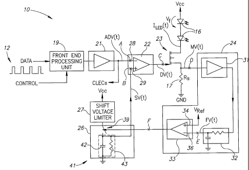
Figure 1 shows a Communication Diode Driver Circuit (CDDC) 10 for
driving one or more Communication Light Emitting Circuits (CLECs) 11 in
accordance with incoming positive digital data pulses 12. Each ' CLEC 11
includes a driver unit 13 for driving a pulsed LED drive current ILED(t) along
a
Communication Light Emitting Branch (CLEB) 14 strapped between a power
supply voltage Vcc and GND. Each CLEB 14 includes a pair of Communication
Diodes (CDs) 16 in series with a sense resistor 17 of low resistance Rs tied
to
ground. Each CLEC 11 further includes a closed loop feedback unit 18 for
continuously monitoring a pulsed monitor voltage MV(t) sensed by the sense
resistor 17 for providing feedback information regarding the instantaneous
values
CA 02576711 2007-02-09
WO 2006/072929 PCT/IL2005/000317
-6-
of the pulsed LED drive current ILED(t), which can be higher or lower than a
predetermined nominal LED drive current IN for selectively illuminating the
CDs
16. The CDDC 10 further includes a Front End Processing Unit 19 for effecting
various digital and/or analog processing functions including inter alia pulse
width limitation, stuck at active digital '1' protection, and the like, and a
fan out
buffer 21 for fanning out the output signal from the Front End Processing Unit
19
to drive all the CLECs 11 with identical input signals, thereby preventing
jitter
and signal distortion therebetween. The Front End Processing Unit 19 inverts
incoming positive digital data pulses to negative digital data pulses since it
is
more robust to clamp to GND than to a relatively noisy voltage supply level.
Figure 2 shows that the driver unit 13 includes a two input terminal shift
amplifier 22 and a Field Effect Transistor (FET) drive transistor 23, and the
closed loop feedback unit 18 includes a toggle unit 24, an integrating unit
26, and
a shift voltage limiter 27. Alternatively, the driver unit 13 can be
implemented
with a bipolar driver transistor, and the like. The shift amplifier 22 has an
inverting input terminal 28 connected to the fan out buffer 21 for receiving
analog data voltage ADV(t) corresponding to the negative digital data pulses
emanating from the fan out buffer 21, and an input terminal 29 connected to
the
integrating unit 26 for receiving a variable shift voltage SV(t) whereupon the
shift amplifier 22 algebraically adds by superposition the analog data voltage
ADV(t) and the shift voltage SV(t) to output a summed up drive voltage DV(t).
The toggle unit 24 includes a measurement amplifier 31 having an
amplification G tapping a monitor voltage MV(t) sensed by the sense resistor
17,
a Low Pass Filter (LPF) 32 for conditioning the amplified monitor voltage
MV(T) to issue a feedback voltage FV(t), and a comparator 33 having an input
terminal 34 connected to a reference voltage VREF where VREF=IN*RskG, and an
inverting input terminal 36 for receiving the feedback voltage FV(t). The LPF
32
can be implemented from a passive RC architecture, a higher order passive
filter,
an active filter that uses various types of amplifiers, and the like. Figure
3A
shows a resultant generally rectangular voltage pulse 37 after being amplified
by
CA 02576711 2007-02-09
WO 2006/072929 PCT/IL2005/000317
-7-
the measurement amplifier 31 pursuant to an incoming digital data pulse.
Figures 3B-3D show that the LPF 32 filters voltage overshoots 38 of amplified
voltage pulses 37 and also shapes them to largely triangular shaped voltage
pulses. The comparator 33 outputs either an ON or OFF digital control state to
the integrating unit 26 as follows: the comparator 33 outputs an ON digital
control state when VREF>FV(t) (see Figure 3B) and conversely an OFF digital
control state when FV(t)>VREF (see Figures 3C and 3D). Figure 3C and Figure
3D show that the maximum voltage of the filtered voltage pulses dictates the
duration that FV(t)>VREF and consequently the duration that the comparator 33
issues the OFF digital control state. The comparator 33 issues a longer OFF
digital control state T2>T1 for the voltage pulse shown in Figure 3D than that
shown in Figure 3C.
The integrating unit 26 includes a switch 39 operated by the toggle unit
24, and a memory device 41 for providing the shift voltage SV(t) to the shift
amplifier 22. The memory device 41 includes a capacitive memory component
42 selectively strapped between the shift voltage limiter 27 and GND to
provide
the shift voltage SV(t), and a resistive memory component 43 in parallel to
the
capacitive memory component 42. ON digital control states, on the condition
that IN>ILED(t), close the switch 39 for continuously charging the capacitive
memory component 42 for continuously increasing the shift voltage SV(t), up to
the shift voltage SV(t)'s maximum value SVmax, as determined by the shift
voltage limiter 27 in the long absence of incoming digital data pulses.
Conversely, OFF digital control states resulting from ILED(t)>IN open the
switch
39 to slowly discharge the capacitive memory component 42 to decrease the
shift
voltage SV(t) via the resistive memory component 43.
Figure 4 shows six Timing Diagrams TD1-TD6 at six circuit points
labeled A, B, C, D, E and F for demonstrating the transient state response of
the
CLEC 11 to nine digital data pulses DP 1, DP2, DP3, ...., DP9 pursuant to a
long
absence of incoming digital data pulses. The Timing Diagram TD1 shows the
analog data voltage ADV(t) at the circuit point A corresponding to the arrival
of
CA 02576711 2007-02-09
WO 2006/072929 PCT/IL2005/000317
-8-
the nine digital data pulses. The Timing Diagram TD2 shows the shift voltage
SV(t) at the circuit point B periodically decreasing stepwise from its maximum
value SV,,,a,, corresponding to the arrival of the nine digital data pulses.
The
Timing Diagram TD3 shows the drive voltage DV(t) at the circuit point C
relative to the threshold drive voltage 44 for continuously illuminating the
CDs
16. The Timing Diagram TD3 shows that the drive voltage DV(t) is greater than
the threshold drive voltage 44 for each and every incoming digital data pulse
for
illuminating the CDs 16. The Timing diagram TD4 shows the monitor voltage
MV(t) at the circuit point D decreasing in a similar fashion as the shift
voltage
SV(t). The Timing Diagram TD5 shows the feedback voltage FV(t) at the circuit
point E relative to the reference voltage VREF and that the feedback voltage
FV(t)
rapidly converges to the reference voltage VREF. In particular, the Timing
Diagram TD5 shows that FV(t)>VREF for the first six digital data pulses DP1,
DP2, ... DP6, VREF>FV(t) for the next two digital data pulses DP7 and DP8, and
FV(t)>VREF for the last digital data pulse DP9. Thus, the Timing Diagram TD5
is
indicative that ILED(t)>IN in the case of the digital data pulses DPl, DP2,
... DP6,
and DP9, and conversely IN>ILED(t) in the case of the digital data pulses DP7
and
DP8. The Timing Diagram TD6 shows that the switch 39 is in its closed state
most of the time and is periodically momentarily opened when FV(t)>VREF,
namely, ILED(t)>IN, to stepwise decrease the shift voltage SV(t). Moreover,
the
Timing Diagram TD6 shows that the duration that the switch 39 is open depends
on the voltage difference FV(t)-VREF on the condition FV(t)>VREF, namely,
ILED(t)>IN=
Figure 5 shows six Timing Diagrams TD11-TD16 at the same six circuit
points labeled A, B, C, D, E and F for demonstrating the steady state response
of
the CLEC 11 to nine digital data pulses DP11, DP12, DP13, ...., DP19 after
having settled to its steady state operation due to a relatively continuous
steady
flow of incoming digital data pulses. In particular, the Timing Diagram TD13
in a
similar manner as the Timing Diagram TD3 shows that the drive voltage DV(t) is
greater than the threshold drive voltage 44 for each and every incoming
digital
CA 02576711 2007-02-09
WO 2006/072929 PCT/IL2005/000317
-9-
data pulse for illuminating the CDs 16 accordingly. Also, the Timing Diagram
TD 15 shows how the LED drive current ILED(t) stabilizes around the nominal
LED drive current IN within a small tolerance, as evidenced by the feedback
voltage FV(t) being generally smaller than the reference voltage VREF,
whereupon
the shift voltage SV(t) slightly increases (see Timing Diagram TD12) but is
cyclically greater than same whereupon the toggle unit 24 issues OFF digital
control states to periodically open the switch 39 (see Timing Diagram TD16)
for
causing slights drops in the shift voltage SV(t) (see Timing Diagram TD12).
While the invention has been described with respect to a limited number
of embodiments, it will be appreciated that many variations, modifications,
and
other applications of the invention can be made within the scope of the
appended
claims. For example, the shift voltage limiter 27 can alternatively be
connected
between the shift amplifier 22 and the integrating unit 26. The memory unit 41
can be implemented by electrical circuits other than a capacitive memory
component 42 in parallel to a resistive memory component 43. The memory unit
41 can be implemented to stepwise increase the shift voltage SV(t) on the
condition ILED(t)<IN instead of continuously increasing same. The comparator
33
may be connected in reverse to the reference voltage VREF and the LPF 32,
thereby requiring that the operation of the integrating unit 26 also be
reversed.