Note: Descriptions are shown in the official language in which they were submitted.
CA 02576772 2007-02-08
WO 2006/023620 PCT/US2005/029352
1
SINGULATION OF RADIO FREQUENCY IDENTIFICATION (RFID)
TAGS FOR TESTING AND/OR PROGRAMMING
BACKGROUND OF THE INVENTION
Field of the Invention
[0001] The present invention relates to high volume testing and programming
of radio frequency identification (RFID) tags, including inlays and labels.
Background Art
[0002] Radio frequency identification (RFID) tags are electronic devices that
may be affixed to items whose presence is to be detected and/or monitored.
The presence of an RFID tag, and therefore the presence of the item to which
the tag is affixed, may be checked and monitored by devices known as
"readers." Readers typically transmit radio frequency signals to which the
tags respond. Each tag can store a unique identification number. The tags
respond to the reader transmitted signals by providing their identification
number, bit-by-bit, so that they can be identified.
[0003] Currently, some RFID tags are assembled and then laminated to the
face sheet of a pressure sensitive laminate. Once laminated, the backside of
the RFID tag is coated with an adhesive, and a release liner is applied. After
the release liner is applied, the tag is printed and/or die cut into the
desired
form factor.
[0004] A tag can be tested either before or after the lamination process.
Testing before or after the lamination process is difficult in a web format,
where tags are formed in an array of tags in a single sheet of material. When
testing tags in a web format, any bad or failed (e.g., non-functional,
malfunctioned) tags have to be removed and replaced with good (e.g.,
functional) tags, which tends to be expensive and time consuming.
[0005] Thus, methods, systems, and apparatuses are needed for testing and
programming tags in high volume webs, while allowing for improved
handling of any failed tags.
CA 02576772 2007-02-08
WO 2006/023620 PCT/US2005/029352
-2-
BRIEF SUMMARY OF THE INVENTION
[0006] Methods, systems, and apparatuses for interacting with radio frequency
identification (RFID) tags are described. In example aspects of the present
invention, tags are interacted with by testing the tags and/or programming the
tags. According to aspect of the present invention, testing and programming
can occur in high volume webs of tags, allowing for improved handling of
failed tags.
[0007] In a first example aspect of the present invention, a system is used to
interact witli a plurality of RFID tags provided in a roll, web, or any other
format. The system supplies the plurality of tags using a supply spool or
other
mechanism, and receives the tags with a collection spool or other mechanism.
A stepper motor or other mechanism can be used to feed the tags to the
collection spool.
[0008] The tags are fed across a surface, so that the surface is in contact
with
the tags. The surface has a first portion and a second portion. The first
portion of the surface is grounded (or coupled to another suitable potential)
to
inhibit operation of tags that are in contact with the first portion. The
second
portion of the surface does not inhibit operation of tags that are adjacent to
the
second portion. A radio frequency (RF) source transmits a RF signal to
interact with a tag adjacent to the second portion of the surface.
[0009] In example aspects, the RF signal may be a signal for testing the tag
and/or a signal for programming the tag.
[0010] In further aspects, the tags can be moved/advanced to move further
tags adjacent to the second portion of the surface so that they may be
interacted with.
[0011] These and other advantages and features will become readily apparent
in view of the following detailed description of the invention. Note that the
Summary and Abstract sections may set forth one or more, but not all
exemplary embodiments of the present invention as contemplated by the
inventor(s).
CA 02576772 2007-02-08
WO 2006/023620 PCT/US2005/029352
-3-
BRIEF DESCRIPTION OF THE DRAWINGS/FIGURES
[0012] The accompanying drawings, which are incorporated herein and form a
part of the specification, illustrate the present invention and, together with
the
description, further serve to explain the principles of the invention and to
enable a person skilled in the pertinent art to make and use the invention.
[0013] FIG. 1 shows a block diagram of an exemplary RFID tag, according to
an embodiment of the present invention.
[0014] FIG. 2 shows a plan view of an example web of tags.
[0015] FIG. 3 shows a plan view of an example grounded surface, according
to an embodiment of the present invention.
[0016] FIG. 4 shows the web of tags of FIG. 2 in contact with the grounded
surface of FIG. 3, according to an example embodiment of the present
invention.
[0017] FIG. 5 shows a cross-sectional view of a radio frequenqy signal
interacting with a tag of a web, according to an example embodiment of the
present invention.
[0018] FIG. 6 shows an example of a high volume tester and programmer,
according to an embodiment of the present invention.
[0019] FIG. 7 shows an example flowchart for interacting with a tags of a web
of tags, according to an embodiment of the present invention.
[0020] The present invention will now be described with reference to the
accompanying drawings. In the drawings, like reference numbers indicate
identical or functionally similar elements. Additionally, the left-most
digit(s)
of a reference number identifies the drawing in which the reference number
first appears.
DETAILED DESCRIPTION OF THE INVENTION
Introduction
[0021] The present invention enables the interaction of an RF signal with
electronic devices, such as tags fabricated in a roll (i.e., a single tag-
width
CA 02576772 2007-02-08
WO 2006/023620 PCT/US2005/029352
-4-
substantially continuous column) or web (i.e., a multi-tag width array of tags
that is substantially continuous) of RFID tags. For example, the interaction
may enable the testing and/or programming of RFID tags, including inlays and
labels, such as ultra-high frequency (UHF) tags. Furthermore, in
embodiments, the present invention allows for the marking of any failed tags
for removal, sorting, disablement, and/or other purposes.
[0022] For illustrative purposes, the description herein primarily relates to
the
testing and programming of RFID tags. However, the invention is also
adaptable to further electronic device types (e.g., electronic devices
including
one or more IC dies or other electrical components mounted thereto), as would
be understood by persons skilled in the relevant art(s) from the teachings
herein.
[0023] FIG. 1 shows a block diagram of an exemplary RFID tag 100,
according to an embodiment of the present invention. As shown in FIG. 1,
RFID tag 100 includes a die 104 and related electronics 106 located on a tag
substrate 116. Related electronics 106 includes an antenna 114 in the present
example. Die 104 can be mounted onto antenna 114 of related electronics
106, or on other locations of substrate 116. As is further described elsewhere
herein, die 104 may be mounted in either a pads up or pads down orientation.
[0024] RFID tag 100 may be located in an area having a large number,
population, or pool of RFID tags present. Tag 100 receives interrogation
signals transmitted by one or more tag readers. According to interrogation
protocols, tag 100 responds to these signals. The response(s) of tag 100
includes information that the reader can use to identify the corresponding tag
100. Once the tag 100 is identified, the existence of tag 100 within a
coverage
area defined by the tag reader is ascertained.
[0025] RFID tag 100 may be used in various applications, such as inventory
control, airport baggage monitoring, as well as security and surveillance
applications. Thus, tag 100 can be affixed to items such as airline baggage,
retail inventory, warehouse inventory, automobiles, compact discs (CDs),
CA 02576772 2007-02-08
WO 2006/023620 PCT/US2005/029352
-5-
digital video discs (DVDs), video tapes, and other objects. Tag 100 enables
location monitoring and real time tracking of such items.
[0026] In the present embodiment, die 104 is an integrated circuit that
performs RFID operations, such as communicating with one or more tag
readers (not shown) according to various interrogation protocols. Exemplary
interrogation protocols are described in U.S. Patent No. 6,002,344 issued
December 14, 1999 to Bandy et al., titled "System and Method for Electronic
Inventory," and U.S. Patent Application No. 10/072,885, filed on February 12,
2002. Die 104 includes a plurality of contact pads that each provide an
electrical connection with related electronics 106.
[0027] Related electronics 106 are connected to die 104 through a plurality of
contact pads of IC die 104. In embodiments, related electronics 106 provide
one or more capabilities, including RF reception and transmission
capabilities,
impedance matching, sensor functionality, power reception and storage
functionality, as well as additional capabilities. The components of related
electronics 106 can be printed onto a tag substrate 116 with materials, such
as
conductive inks. Examples of conductive inks include silver conductors 5000,
5021, and 5025, produced by DuPont Electronic Materials of Research
Triangle Park, N.C. Other example materials or means suitable for printing
related electronics 106 onto tag substrate 116 include polymeric dielectric
composition 5018 and carbon-based PTC resistor paste 7282, which are also
produced by DuPont Electronic Materials of Research Triangle Park, N.C.
Other materials or means that may be used to deposit the component material
onto the substrate would be apparent to persons skilled in the relevant art(s)
from the teachings herein.
[0028] As shown in FIG. 1, tag substrate 116 has a first surface that
accommodates die 104, related electronics 106, as well as further components
of tag 100. Tag substrate 116 also has a second surface that is opposite the
first surface. An adhesive material and/or backing can be included on the
second surface. When present, an adhesive backing enables tag 100 to be
attached to objects, such as books, containers, and consumer products. Tag
CA 02576772 2007-02-08
WO 2006/023620 PCT/US2005/029352
-6-
substrate 116 is made from a material, such as polyester, paper, plastic,
fabrics
such as cloth, and/or other materials such as commercially available Tyvec .
[0029] Embodiments of the present invention are applicable to all types of
tags, including inlays and labels. A "tag inlay" or "inlay" is used generally
to
refer to an assembled RFID device that generally includes a integrated circuit
chip and antenna formed on a substrate. A "label" is used generally to refer
to
an inlay that has been attached to a pressure sensitive adhesive (PSA)
construction, or laminated and then cut and stacked for application through in-
mould, wet glue or heat seal application processes, for example. A variety of
label types are contemplated by the present invention. In an embodiment, a
label includes an inlay attached to a release liner by pressure sensitive
adhesive. The release liner may be coated with a low-to-non-stick material,
such as silicone, so that it adheres to the pressure sensitive adhesive, but
may
be easily removed (e.g., by peeling away). After removing the release liner,
the label may be attached to a surface of an object, or placed in the object,
adhering to the object by the pressure sensitive adhesive.
[0030] In some implementations of tags 100, tag substrate 116 can include an
indentation, "cavity," or "cell" (not shown in FIG. 1) that accommodates die
104. An example of such an implementation is included in a "pads up"
orientation of die 104.
[0031] Volume production of RFID tags, such as tag 100, is typically
accomplished on a printing web based system. For example, in such a system,
the tags are assembled in a roll or web of substrates, which may be a sheet of
substrates, a continuous roll of substrates, or other group of substrates. For
instance, FIG. 2 shows a plan view of an example web 200 that is a continuous
roll type. As shown in FIG. 2, web 200 may extend further in the directions
indicated by arrows 210 and 220. Web 200 includes a plurality of tags 100a-p.
In the example of FIG. 2, the plurality of tags 100a-p in web 200 is arranged
in
a plurality of rows and columns. The present invention is applicable to any
number of rows and columns of tags, and to other arrangements of tags, in a
roll, web, or other format.
CA 02576772 2007-02-08
WO 2006/023620 PCT/US2005/029352
-7-
[0032] During or after the manufacture of a tag, such as tag 100, the tag may
processed by a system that interacts with the tag. For example, the system
may test and/or program the tag. For instance, the tag may be tested to check
for defects in functionality, such as its ability to detect a reader
interrogation,
and to respond. Furthermore, data may be directly encoded in, or transmitted
to the tag (e.g., by a reader), to be stored on the tag. For example, the data
may be an identification number for the tag.
[0033] On a web, such as web 200, RFID tags are typically
assembled/positioned as close to each other as possible to maximize
throughput, thus making the process of reading and testing individual tags
difficult. Because of the close spacing, it is very difficult to localize a
radiated
(e.g., radio frequency) reader field to excite only one tag. Thus, interacting
with a specific tag can be difficult: Furthermore, typically, an assembly line
must be customized to accommodate the roll or web and the specific type of
tags. The testing/programming process becomes even more difficult and
expensive considering that RFID tags, for example, come in different forms,
sizes and shapes.
[0034] In an embodiment of the present invention, an apparatus tests and/or
programs a RFID tag in a continuous web of RFID tags, such as in web 200,
by exposing it to a radio frequency (RF) test signal, while nearby RFID tags
of
the web are isolated from the RF test signal. In this manner, a specific tag
can
be tested, while nearby tags are prevented from also responding to the RF test
signal. Furthermore, in embodiments, the apparatus accommodates different
types of RFID tags without the need for significant changes to the assembly
line.
[0035] FIG. 3 shows a plan view of an example contact surface 302, according
to an embodiment of the present invention. As shown in FIG. 3, contact
surface 302 has a first portion 304 and a second portion 306. First portion
304
of contact surface 302 can be made from any electrically conductive material,
such as a metal. Second portion 306 can be an opening through contact
CA 02576772 2007-02-08
WO 2006/023620 PCT/US2005/029352
-8-
surface 302, or can be spanned by an electrically non-conductive material,
such as a sheet of plastic, glass, a polymer, etc.
[0036] When in use, contact surface 302 is contacted with a roll or web of
tags. For example, FIG. 4 shows a plan view of web 200 of FIG. 2 in contact
with contact surface 302, according to an example embodiment of the present
invention. In FIG. 4, contact surface 302 is not shown, only an outline of
second portion 306 is indicated by a dotted line. This is because contact
surface 302 is in contact with the opposite side of web 200, not shown in FIG.
4, so contact surface 302 is not visible in FIG. 4. In FIG. 4, web 200 is
disposed across contact surface 302 so that a large area of web 200 is in
contact with contact surface 302.
[0037] In an embodiment, contact surface 302 is electrically coupled to an
electrical potential, such as a ground potential or other potential, to
electrically
hold tags of web 200 that are in contact with first portion 304 at the
potential.
For example, in FIG. 4, tags 100a-e,g-p in contact with first portion 304 are
grounded (or held at another potential) by first portion 304. Because the tags
are held at the potential, they are caused to be in a non-operational state.
For
example, electrically conductive portions of the tags of web 200, such as
their
antennas, may be held at the potential due to contact with first portion 304
of
contact surface 302. If the tags are passive tags (i.e., no onboard power
source), they cannot receive power from the RF signal, and are thus not
operational. Note that although the potential may be generally referred to as
a
ground potential herein, the potential can be any potential that causes tags
coupled thereto to be non-operational (e.g., not able to respond to an RF test
and/or programming signal).
[0038] FIG. 5 shows a cross-sectional view of a radio frequency signal 502
interacting with tag 100f of web 200, according to an example embodiment of
the present invention. As shown in FIG. 5, tags 100b, 100j, and other tags of
web 200 are in contact with first portion 304 of contact surface 302. Thus,
these tags are inhibited from operation by contact surface 302. However, as
shown in FIGS. 4 and 5, tag 100f is adjacent to second portion 306 of contact
CA 02576772 2007-02-08
WO 2006/023620 PCT/US2005/029352
-9-
surface 302. Thus, the operation of tag 100f is not inhibited, because second
portion 306 does not inhibit its operation. Tag 100f can therefore be
interacted
with by a RF signal 502, transmitted by an antenna 506 of a RF signal source
504, without interference from unwanted responses by other tags 100 of web
200. This is because, as described above, second portion 306 is an opening
through contact surface 302, or an electrically non-conductive material, so
does not cause tag 100f to be inhibited.
[0039] RF signal 502 may include a test signal and/or a programming signal.
RF signal source 504 can be a RFID reader, for example. Thus, in an
embodiment, RF signal source 504 can communicate according to any RFID
communication protocol, including those described elsewhere herein, a binary
traversal protocol, a slotted aloha protocol, Class 0, Class 1, and EPC Gen 2,
for example.
[0040] Note that in the example embodiment of FIG. 5, antenna 506 transmits
RF signal 502 through contact surface 302 to tag 100f. RF signal 502 passes
through second portion 306. In such an embodiment, contact surface 302 acts
as a RF shield, to shield RF signa1502 from tags 100b and 100j. Furthermore,
in such an embodiment, second portion 306 is an opening or a non-RF
shielding material.
[0041] Note that contact surface 302 may be a surface of an enclosure. For
example, the enclosure may enclose antenna 506 to provide further shielding
of RF signa1502.
[0042] As described above, in embodiments, the present invention
accommodates different types of RFID tags without the need for changes to
the assembly line. For example, to accommodate different tag sizes, an
operator or automated mechanism can replace contact surface 302 with a
second portion 306 of a size to accommodate the different tag size if
required.
Alternatively, contact surface 302 may be computer controlled to vary the size
of second portion 306 as required, such as through the use of automated
shutters, etc., through contact surface 302. Thus, little to no changes to the
assembly line are required.
CA 02576772 2007-02-08
WO 2006/023620 PCT/US2005/029352
-10-
[0043] FIG. 6 shows a view of an example tester and/or programmer 600 for
interacting with tags (hereinafter "tester"), according to an embodiment of
the
present invention. As shown in FIG. 6, tester 600 includes a supply spool 602,
a web 604, a collection spool with stepper motor 606, an antenna 610, a reader
612, a computer 614, a marking device 616, a database 618, a contact surface
620, and an enclosure 670.
[0044] In the present embodiment, tester 600 is an automated machine and is
controlled by computer 614. One or more elements of tester 600 can be
enclosed by enclosure 670. For example, as shown in FIG. 6, reader 612,
antenna 610, supply spool 602, and stepper motor 606 are enclosed by
enclosure 670. In an embodiment, enclosure 670 is a cabinet made from an
electromagnetic signal shielding material, such as a metal, and/or is made
from other materials.
[0045]. In an embodiment, human intervention may be used to set up tester
600. In an embodiment, an operator identifies a roll or web of RFID tags to be
tested or programmed, and loads tester 600 with a supply spool 602 containing
the identified web (or roll). Computer 614 communicates with database 618
for information regarding the tags of the identified web. Database 618
uploads information such as testing and programming specifications, tag
physical characteristics, and/or other information related to the testing and
programming of tags (such as inlays or labels) to computer 614. Although
shown separately in FIG. 6, database 618 can be maintained in computer 614.
[0046] In an embodiment, RFID tags enter the testing and/or programming
phase in the continuous web form of web 604 contained on supply spool 602.
Alternatively, web 604 may be supplied in the form of discrete rectangular
sheets of tags, or in other forms. Supply spool 602 supplies web 604 to tester
600 for testing and/or programming. Web 604 is moved across contact
surface 620 and across an ungrounded area 622 of contact surface 620 to
collection spool 606. Contact surface 620 provides an electrical ground (or
other suitable potential) contact to ground the portion of the RFID articles
of
web 604 in contact with contact surface 620. Thus, ungrounded portion 622 is
CA 02576772 2007-02-08
WO 2006/023620 PCT/US2005/029352
-11-
an example of second portion 306 of FIG. 3, and the remainder of contact
surface 620 is an example of first portion 304 of FIG. 3.
[0047] In an embodiment, contact surface 620 is a planar or curved metal
shield, but can have shapes and configurations. For example, contact surface
620 may be a portion of enclosure 670, such as a top portion of enclosure 670,
as shown in FIG. 6, configured similarly to a cabinet or table. Alternatively
or additionally, contact surface 620 may comprise at least one metal clamp or
other grounding instrument that clamps on a portion of web 604 where
electrical grounding is desired. In yet another embodiment, contact surface
620 is a conveyor belt with metal contact regions for grounding tags in
contact
with the contact regions. In embodiments, various other techniques known in
the art can be used to electrically ground materials of web 604.
[0048] The grounding of web 604 prevents interaction of nearby RF
signals/fields with tags of web 604. However, at any particular moment, a
portion 624 of web 604 is desired to be tested and/or programmed. Web
portion 624 is positioned adjacent to ungrounded portion 622 of contact
surface 620 to be tested and/or programmed. Web portion 624 comprises one
or more tags, depending upon the configuration of the ungrounded area 622
and on the testing and programming specifications. Web portion 624 is not
grounded (due to ungrounded portion 622 of contact surface 620), and thus
can be interacted with. In the embodiment of FIG. 6, ungrounded area 622 is
an opening 626 over which web 604 traverses. Thus, web portion 624 is freed
from contact with ground, thereby allowing it to be tested and/or programmed
by a RF field.
[0049] In an embodiment, opening 626 can be variably adjusted in size and/or
shape to accommodate different types of RFID articles to be tested. The
adaptability of the size and/or shape of opening 626 allows tester 600 to be
adaptable, thus eliminating the need for specific dies or testing machines for
a
particular RFID article. In addition, the adaptability of opening 626 allows
for
more accurate control of the exposure of the RF field to web portion 624. This
minimizes or eliminates the effect on adjacent tags of web 604.
CA 02576772 2007-02-08
WO 2006/023620 PCT/US2005/029352
-12-
[0050] In another embodiment, ungrounded area 622 includes a structure
made of an electrically nonconductive material. Thus, in an embodiment, web
604 is supported or held by the material of ungrounded area 622. For
example, if the contact surface 620 is a metal shield, then part of the metal
shield over which web 604 traverses can be made of an electrically
nonconductive material, thereby creating an ungrounded portion of web 604.
In yet another embodiment, the ungrounded area may include a clamp made of
nonconductive material, or is another mechanism or instrument for decoupling
web portion 624 from ground. For example, ungrounded area 622 may
include a non-electrically conductive wheel or bump, etc., to raise web
portion
624 from contact with contact surface 620.
[0051] In FIG. 6, the testing and/or programming is accomplished by exposure
to a RF field. Antenna 610 emits an RF signal generated by reader 612.
Reader 612 can be a conventional tag reader, or can be a reader designed for
use in a tag test and/or programming environment. The characteristics of the
RF field are controlled by reader 612, which is controlled by computer 614. In
the embodiment of FIG. 6, antenna 610 is located on the opposite side of
contact surface 620 from which web 604 is located. In such a configuration,
contact surface 620 acts both as a grounding mechanism and as a RF shield for
web 604. However, in alternative embodiments, antenna 610 can be located
elsewhere, including on the same size of contact surface 620 as web 604.
[0052] In an embodiment, it may be desirable to mark a tested and/or
programmed RFID article in the event a RFID article fails a test and/or fails
to
be programmed, or for other reasons. In such an embodiment, tester 600
includes marking device 616 to mark a tag on web 604 for later identification.
Once a tag is marked, it can be identified for sorting, removal, retesting,
recycling, or any other purpose. Marking device 616 is controlled by
computer 614. In an embodiment, computer 614 tracks a tag to be marked as
it is moved with web through tester 600. This allows for flexibility in
placing
marking device 616 at or downstream from the testing and/or programming
stage while maintaining the location of the tag to be marked.
CA 02576772 2007-02-08
WO 2006/023620 PCT/US2005/029352
-13-
[0053] In an embodiment, the marking device 616 is a residue depositing
device that deposits an ink, paint, or any other staining or marking material.
In yet another embodiment of the present invention, the marking device 616 is
a punching device. Such punching device may punch a hole partially or
wholly through the tag being marked, including making an indentation in the
tag.
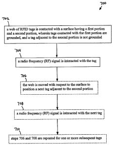
[0054] FIG. 7 shows an example flowchart 700 for interacting with a tags of a
web of tags, according to an embodiment of the present invention. For
example, the structural embodiments described herein may operate according
to flowchart 700 in particular applications. Although described in terms of a
web of tags, flowchart 700 may be applied to a plurality of tags supplied in
any format, including a roll. Other structural and operational embodiments
will be apparent to persons skilled in the relevant art(s) based on the
following
discussion related to flowchart 700. The steps shown in FIG. 7 do not
necessarily have to occur in the order shown. The steps of FIG. 7 are
described in detail below.
[0055] Flowchart 700 begins with step 702. In step 702, a web of RFID tags
is contacted with a surface having a first portion and a second portion,
wherein
tags contacted with the first portion are grounded, and a tag adjacent to the
second portion is not grounded. For example, the web may be a web similar
to web 200 shown in FIG. 2. Furthermore, in an embodiment, the surface can
be contact surface 302 shown in FIG. 3. Contact surface 302 has a first
portion 304 that is grounded, and a second portion 306. FIG. 4 shows a tag
100f adjacent to second portion 306 that is not grounded. In another
embodiment, the surface of step 702 may be contact surface 620 shown in
FIG. 6.
[0056] In step 704, a radio frequency (RF) signal is interacted with the tag.
For example, FIG. 5 shows an RF signal 502 interacting with tag 100f. FIG. 6
shows an antenna 610 that can transmit an RF signal to interact with a tag
located in web portion 624 of web 604. The RF signal may include a test
signal to test functionality/operation of the tag and/or may include a
CA 02576772 2007-02-08
WO 2006/023620 PCT/US2005/029352
-14-
programming signal to program the tag. For example, the programming signal
may be used to write an identification number or other data to the tag.
Computer 614 may be present to control reader 612.
[0057] Steps 706, 708, and 710 are optional. These steps may be performed in
embodiments where a plurality of tags are to be interacted with in a web.
[0058] In step 706, the web is moved with respect to the surface to position a
next tag adjacent to the second portion. For example, FIG. 6 shows a supply
spool 602 and collection spool with stepper motor 606 that may be used to
move a web with respect to a surface, such as contact surface 620. Computer
614 may be present to control stepper motor 606. The web is moved to
position a next tag, such as tag 100b shown in FIG. 5, adjacent to the second
portion (e.g., not grounded) of the surface. Furthermore, in an embodiment,
contact surface 620 may be additionally or alternatively moved. Still further,
contact surface 620 may have a plurality of controllable ungrounded areas 622
arranged to span a width of web 604. For example, the plurality of
controllable ungrounded areas 622 may be activated/opened sequentially by
computer 614, to sequential test tags across the width of web 604 (e.g,. to
sequentially test tags 100a-d across the width of web 200 shown in FIG. 2).
[0059] In step 708, a radio frequency (RF) signal is interacted with the next
tag. For example, antenna 610 shown in FIG. 6 can transmit an RF signal to
interact with the next tag located in web portion 624 of web 604.
[0060] In step 710, steps 706 and 708 are repeated for one or more subsequent
tags. Thus, according to step 710, any number of tags in a web can be
interacted with as desired by the particular application, including
interacting
serially with the tags of the web in a continuous fashion until all of the
tags of
the web have been interacted with. Furthermore, in embodiments, multiple
tags may be simultaneously interacted with in a web, using multiple
interaction stations, such as shown in FIGS. 5 and 6. The stations may be RF
shielded from each other, such as by using multiple enclosures 670, to prevent
interference.
CA 02576772 2007-02-08
WO 2006/023620 PCT/US2005/029352
-15-
[0061] It should be understood that elements of the systems described herein
can be implemented in hardware, firmware, software, or a combination
thereof. For example, hardware, firmware, or module of software can perform
one or more of the illustrated components of FIG. 6 (e.g., computer 614,
reader 612) and/or steps of FIG. 7. For example, the hardware, firmware,
software, or any combination thereof, may include algorithms for testing
and/or programming tags, including the control of reader 612, stepper motor
606, and/or marking device 616.
[0062] In this document, the terms "computer program medium" and
"computer usable medium" are used to generally refer to media such as a
removable storage unit, a hard disk installed in hard disk drive, and signals
(i.e., electronic, electromagnetic, optical, or other types of signals capable
of
being received by a communications interface): These computer program
products are means for providing software to a computer system. The
invention, in an embodiment, is directed to such computer program products.
[0063] In an embodiment where aspects of the present invention are
implemented using software, the software may be stored in a computer
program product and loaded into computer system using a removable storage
drive, hard drive, or communications interface. The control logic (software),
when executed by a processor, causes the processor to perform the functions
of the invention as described herein.
[0064] According to an example embodiment, a computer executes computer-
readable instructions to control one or more of a stepper motor, a reader, and
a
marker device. For instance, a computer may control movement of a roll or
web to test the various tags in the web by controlling the stepper motor.
Furthermore, the computer may instruct the reader to generate test and/or
programming signals synchronized with the movement of the web. Tags may
be communicated with by the reader according to any suitable communication
protocols, including binary traversal protocols, slotted aloha protocols,
Class
0, Class 1, EPC Gen 2, those mentioned elsewhere herein, and future
CA 02576772 2007-02-08
WO 2006/023620 PCT/US2005/029352
-16-
protocols. Still further, the computer may control the marking of defective
tags by the marking device.
[0065] In another example embodiment, aspects of the present invention are
implemented primarily in hardware using, for example, hardware components
such as application specific integrated circuits (ASICs). Implementation of
the hardware state machine so as to perform the functions described herein
will be apparent to one skilled in the relevant art(s).
Conclusion
[0066] While various embodiments of the present invention have been
described above, it should be understood that they have been presented by way
of example only, and not limitation. It will be apparent to persons skilled in
the relevant art that various changes in form and detail can be made therein
without departing from the spirit and scope of the invention. Thus, the
breadth
and scope of the present invention should not be limited by any of the above-
described exemplary embodiments, but should be defined only in accordance
with the following claims and their equivalents: