Note: Descriptions are shown in the official language in which they were submitted.
CA 02577117 2007-02-12
WO 2006/135393 PCT/US2005/028967
Method and System for Optimizing Surface Enhanced Raman Scattering
STATEMENT REGARDING FEDERALLY SPONSORED
RESEARCH OR DEVELOPMENT
This invention was made with government support under Grant F49620-03-C-0068
awarded by Air Force Office of Scientific Research. The United States
government has certain
rights in the invention.
FIELD OF THE INVENTION
The present invention relates generally to a method and system for performing
analysis
of Surface Enlianced Raman Scattering (SERS) on an analyte. More particularly,
aspects of the
present invention relate to plasmonic nanoparticle substrates used for surface
enhanced Raman
scattering. Still more particularly, aspects of the present invention relate
to selecting plasmonic
nanoparticle substrates that maximize the electromagnetic field strength at a
specific frequency.
BACKGROUND OF THE INVENTION
Since the initial discovery of (SERS), understanding how the local
electromagnetic
environment enhances the substrate-adsorbate complex's spectral response has
been of central
importance. It has become increasingly evident that plasmon resonances of the
metallic
substrate provide intense, local optical-frequency fields responsible for
SERS.
The lack of reliable techniques for controlling the properties of the local
field at the
metal surface has been a major experimental limitation in the quantification
and understanding
of SERS. A striking example of this is the series of experiments reporting
enormous SERS
enhancements of 1012 -1015 for dye molecules adsorbed on surfaces of
aggregated Au and Ag
colloid films. The SERS enhancements reported in these experiments have been
attributed to
localized plasmons, or "hot spots," occurring randomly across this film that
fortuitously
provide the appropriate electromagnetic nanoenvironment for large SERS
enhancements. More
recent studies have shown that localized plasmons giving rise to very large
field enhancements
can be formed at the junctions between adjacent nanoparticles. These plasmons
can be
described within the plasmon hybridization picture as dimer resonances.
Likewise, self-similar
geometries also provide a means for developing large field enhancements.
Several experimentally realizable geometries, such as triangles, nanorings,
and
nanoshells, support well-defined plasmon resonances whose frequencies can be
controlled by
judicious modification of the geometry of the nanoparticle. Each of these
nanostructured
geometries offers its own unique near field properties: plasmon resonant
frequency, spatial
1
CA 02577117 2007-02-12
WO 2006/135393 PCT/US2005/028967
distribution of the near field amplitude across the surface of the
nanostructure, orientation
dependence on polarization of the incident light wave, and spatial extent of
the near field.
The near field properties of metallic nanoparticles can be calculated very
precisely by a
variety of methods, such as analytic Mie scattering theory for high-symmetry
geometries, and
numerical methods such as the discrete dipole approximation (DDA) and the
finite difference
time domain (FDTD) methods for nanoscale objects of reduced symmetry. It is
thus possible to
approach a convergence between the electromagnetic fields determined
theoretically and those
achievable experimentally for an increasing range of nanoscale metallic
geometries, which will
ultimately lead to the development of precisely designed nano-optical
components for SERS
and other applications. Such a near infrared optimized nanosensor for
electromagnetic
emission spectroscopy is likely to be of utility in a variety of biological
studies and biomedical
applications, such as bioassays, intracellular spectroscopy and molecular
level diagnosis of
early stage cancer.
SERS has been previously performed using solid metal films, isolated metal
nanoparticles, and aggregates of nanoparticles. The plasmon resonance peak of
metal
nanoparticles can be altered to a limited degree by increasing the size of the
metal nanoparticle
or by aggregation of such particles. For example, the plasmon resonance peak
for gold
nanoparticles is generally approximately 525 nm, but will increase as the
particles are made
larger (e.g., increasing to approximately 600 nm as the particles are grown to
a diameter of 120
nm). In order to achieve a plasmon resonance peak at longer excitation
wavelengths, such as
633 nm or 785 nm, larger aggregates of particles are required. These longer
wavelengths are
useful for interrogation of biological or other samples where there is a
background
autofluorescence at lower wavelengths.
Isolated solid nanoparticles at their respective plasmon resonance (-525 nm
for gold,
-430 nm for silver) have reported enhancement factors up to 10~6. In order to
perform SERS
at wavelengths greater than the intrinsic plasmon resonance of the isolated
colloid, it is
necessary to aggregate the colloid.
The work of vanDuyne and others has identified "hot spots" in the aggregated
colloids
at these greater wavelengths; the SERS from the analyte at selected places
within the field, or a
"hot spot", has achieved reported enhancements of greater than 10~14. However,
these "hot
spots" are believed to be the result of a unique, and difficult to reproduce,
association between
the analyte and the aggregated particles at that particular location. This
effect was further
demonstrated by the work of Zhu.
2
CA 02577117 2007-02-12
WO 2006/135393 PCT/US2005/028967
Accordingly, there is a need for a reproducible method of SERS with
significant
enhancements at various excitation wavelengths.
As demonstrated by embodiments of this invention, the nanoparticle-based
substrates
described herein may be tunable to achieve strong electromagnetic fields at
desired excitation
wavelengths, resulting in significant enhancements from the individual
nanoparticles rather
than aggregates. Additionally, the electromagnetic peak can be tuned to
wavelengths between
the excitation and emission frequencies as desired. As a result, this
invention demonstrates a
platform for SERS from individual nanoparticles that can achieve enhancements
of >l0~7 at
the desired wavelengths, including wavelengths at 633nm or greater.
SUMMARY OF TH.E INVENTION
A substrate for enhanced electromagnetic spectroscopy of an analyte, the
substrate
comprises a solid support and a plurality of individual nanoparticles affixed
to the solid
support, wherein the individual nanoparticles are designed to have an
increased
electromagnetic field strength that is between a first frequency of an
incident electromagnetic
radiation and a second frequency of Raman response from the analyte and
wherein the
Raman response is enhanced by the individual nanoparticles. The individual
nanoparticles
may have a plasmon resonance frequency that is between a first frequency of an
incident
electromagnetic radiation and a second frequency of Raman response from the
analyte and
may enhance the Raman response by a factor of at least 107.
The nanoparticles may be nanospheres comprising a shell surrounding a core
material
with a lower conductivity than the shell_ material, and the thickness of the
core material and the
thickness of the shell material may be selected to generate the plasmon
resonance frequency.
The core may comprise at least one of the following: silicon dioxide, gold
sulfide, titanium
dioxide, polymethyl methacrylate (P1VIlVIA), polystyrene, hydrogels, and
macromolecules such
as dendrimers. The shell comprises at least one of the following: gold,
silver, copper,
platinum, palladium, lead, and iron.
The solid support may comprise at least one of the following: an inert glass,
a metal, a
metal film, an oxide, or a living cell, and may be a reflective surface.. The
substrate of claim 1
wherein the nanoparticle may be bonded to the solid support covalently,
electrostatically, or via
adsorption. The nanoparticle may be selected from among spherical or
elliptical shells, hollow
nanoshells, multilayer nanoshells, nanorods, nanostars nanotriangles, and
nanocubes.
The wavelength of the incident electromagnetic radiation is preferably between
200nm and 20
microns and may be selected from among wavelengths that reduce the
electromagnetic
3
CA 02577117 2007-02-12
WO 2006/135393 PCT/US2005/028967
emission from molecules other than the analyte to be detected. The analyte may
be a powder,
or may be suspended in a liquid and the liquid may be biological fluid such as
blood, cerebral
spinal fluid, phlegm, mucous, or urine.
In other embodiments, a substrate for surface enhanced Raman spectroscopy of
an
analyte comprises a solid support and a plurality of individual nanoparticles
affixed to the solid
support, wherein the individual nanoparticles are designed to have a peak
electromagnetic field
strength when illuminated with an excitation wavelength that is equal to or
greater than 600
nm.
BRIEF DESCRIPTION OF THE DRAWINGS
Figure 1 is a graph of the electromagnetic field (EMF) of multiple nanospheres
at
different wavelengths.
Figure 2 is a graph of the electromagnetic field (EMF) of multiple nanospheres
at
different wavelengths.
Figure 3 is a graph of Raman spectra.
Figure 4 is representation of different nanoshell densities.
Figure 5 is a table of nanoshell densities and clusters.
Figure 6 is graph of absoprtion spectra for different nanoshell densities.
Figure 7 is a graph of Raman spectra.
Figure 8 is graph of Raman intensity versus density.
Figure 9 is a display of calculated SERS optimization factor shown as a
function of core
radius and shell thickness.
Figure 10 is a comparison of Raman modes to theoretical calculations.
Figure 11 is a table of Raman enhancement as a function of core radius and
shell
thickness.
Figure 12 is a display of extinction for smooth and rough nanoshells.
DETAILED DESCRIPTION OF THE PREFERRED EMBODIMENT
Embodiments of the present invention include methods and apparatus for
performing
SERS analysis by maximizing a specific Raman mode or frequency of interest for
an analyte
exposed to incident electromagnetic radiation. One aspect of an embodiment of
the present
invention comprises choosing a specific geometric configuration for a
nanoparticle, such as a
nanosphere with a dielectric core and a conducting metallic shell, in order to
maximize the
inelastic electromagnetic emission. For example, by varying the core radius
and / or the
thickness of the shell, the electromagnetic field strength of the nanosphere
can be altered in
both the near-field and far-field regions for a given frequency. In another
aspect of an
4
CA 02577117 2007-02-12
WO 2006/135393 PCT/US2005/028967
embodiment of the present invention, the incident electromagnetic radiation
frequency is
selected so that the nanoparticle's maximum electromagnetic field strength is
at a frequency
between the incident electromagnetic radiation frequency and the frequency of
the inelastic
electromagnetic emission from the analyte. Embodiments of the present
invention comprise
methods incorporating the above-described steps to maximize the Raman
response, as well as
systems for performing such steps.
Research has indicated that the highest Raman response is obtained by
maximizing the
nanosphere's electromagnetic near-field strength at the wavelength
corresponding to the
midpoint of the excitation electromagnetic radiation frequency and the
frequency of the Raman
response of interest. Because the nanoparticle's electromagnetic field
strength at a given
wavelength will depend on the nanoparticle geometry, the amplitude of the
inelastic
electromagnetic emission is also dependent upon such geometry. As a result, a
specific Raman
response mode can be maximized by selecting the nanoparticle geometry that
yields the highest
electromagnetic field at the midpoint of the excitation (or incident)
electromagnetic radiation
frequency and the Raman response mode frequency. With regards to nanospheres,
the core
radius and shell thickness, as well as the materials of construction, can be
selected to yield the
maximum electromagnetic field at the midpoint frequency, thereby producing the
maximutn
inelastic electromagnetic emission from the analyte.
For the sake of simplicity, the following discussion of embodiments of the
present
invention includes nanospheres with a dielectric core and a conducting shell
as an example of a
nanoparticle and a laser as a source for electromagnetic radiation.
Embodiments of the present
invention are not limited to such features and may include other nanoparticles
such as elliptical
shells, hollow nanoshells, nanorods, nanostars, nanotriangles, and nanocubes.
The development of nanospheres comprising a non-conductive inner core and an
electrically conductive outer shell is well known in the art and is described
in U.S. Patent
6,344,272 by Oldenburg, et al. (hereinafter the '272 Patent), which is hereby
incorporated by
reference.
The use of an optical device as a support for a thin film formed by a matrix
containing
resonant nanoparticles is disclosed in U.S. Patent 6,778,316 by Halas, et al.
(hereinafter the
'316 Patent), also incorporated by reference.
The ability to shift the plasmon resonance of a nanosphere by adjusting the
core:shell
ratio is disclosed in U.S. Patent 6,699,724, also incorporated by reference.
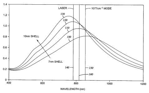
Referring now to Figure 1, a graph is shown displaying the electromagnetic
field (EMF)
of multiple nanospheres at different wavelengths. The EMF measurements
displayed in Figure
5
CA 02577117 2007-02-12
WO 2006/135393 PCT/US2005/028967
1 were taken with air as a medium and correspond to nanospheres with a silica
core with an 81
nm radius and silver shells with varying thicknesses ranging from 7 nm to 10
nm. A graph 100
corresponds to a nanosphere with a 7 nm shell, a graph 110 corresponds to a
nanosphere with
an 8 nm shell, a graph 120 corresponds to a nanosphere with a 9 nm shell and a
graph 130
corresponds to a nanosphere with a 10 nm shell.
A line 140 representing the 782 nm laser excitation frequency and a line 150
representing the 1077 cni 1 Raman mode shift (which corresponds to 854 nm in
this
embodiment) are also displayed on Figure 1. A line 160 is depicted at 818 nm,
the midpoint
between the 782 nm excitation frequency and the 854 nm frequency corresponding
to the 1077
cm 1 Raman mode shift.
As previously mentioned, research has indicated that the maximum response for
a
specific Raman mode shift is obtained by maximizing the electromagnetic field
for the
frequency at the midpoint of the excitation frequency and the Raman mode shift
frequency. In
the graph shown in Figure 1, it can be seen that for the particular nanoshell
thicknesses
displayed, the 10 nm shell nanosphere possesses the maximum electromagnetic
field at the 818
nm midpoint frequency. Therefore, the 10 nm shell nanosphere will produce a
greater response
for the 1077 cm 1 Raman mode shift and 782 nm excitation laser than the other
nanosphere
shell thicknesses displayed in Figure 1.
It should be noted that while the parameters used in Figure 1 resulted in the
thickest
nanoshell being the optimum configuration, such is not always the case. If the
midpoint is
shifted to a higher frequency (due to either an increase in the incident light
frequency or a
change in the Raman mode of interest), it is possible that the 10 nm shell
will not yield the
highest EMF at the frequency of interest.
For example, now referring to Figure 2, the EMF graphs are shown for the same
set of
nanosphere parameters displayed in Figure 1. Graphs 100, 110, 120 and 130
represent EMF
measurements for 7 nm, 8 nm, 9 nm, and 10 nm shell thicknesses, respectively.
However, as
shown in Figure 2, if the incident light frequency is set at 854 nm
(represented by a line 240),
the 1077 cm 1 Raman mode shift is now at 940 nm (represented by a line 250),
resulting in a
midpoint at 897 nm (represented by a line 260). As shown, line 260 intersects
plots 100, 110,
120 and 130 at differing EMF values. It can be seen from Figure 2 that line
110 intersects line
260 at the highest EMF value. Therefore, for the various shell thicknesses
listed in Figure 2,
the 8 nm shell thickness represented by line 110 will yield the greatest Raman
response for the
1077 cm 1 shift with an excitation frequency of 854 nm. It should be noted
that other
6
CA 02577117 2007-02-12
WO 2006/135393 PCT/US2005/028967
nanosphere configurations besides those depicted in Figure 2 may result in a
higher EMF and
Raman response.
As demonstrated in the discussion of Figures 1 and 2, if the excitation
frequency and
Raman frequency are known, as well as the EMF graphs for a group of
nanospheres, a
nanosphere can be selected from the group to yield the maximum Raman response
for an
analyte. Similarly, if a specific nanosphere must be used for a SERS analysis
and the Rainan
shift for an analyte is known, the frequency of the excitation laser can be
selected so that the
maximum EMF value of the nanosphere is between the incident light frequency
and the Raman
response frequency. For example, referring back now to Figure 1, it can be
seen that the peak
EMF value for the 8 nm shell (represented by line 110) is at or very near the
818 nm midpoint
of the excitation and 1077 cm 1 shift frequencies. In this case, the 782 nm
excitation frequency
would be the optimum frequency for the 1077 cm"1 Raman mode used with an 8 nm
shell
nanosphere.
Independent control of the core and shell dimensions of nanoshells offers a
valuable
opportunity to systematically control the plasmon resonance frequency of a
nanostructure and
therefore maximize the electromagnetic near-field strength at a specific
frequency. The
plasmon resonant frequency of a nanoshell can be tuned from the visible region
of the spectrum
into the infrared, giving rise to a host of useful applications. The plasmon
resonances for Au
and Ag nanoshells in this wavelength region are quite similar. The tunable
plasmon frequency
allows one skilled in the art to design substrates with plasmon resonances
shifted far away from
the electronic resonances of an adsorbate molecule, providing a strategy for
separating the
electromagnetic from the chemical effects in SERS. In addition, the spherical
symmetry of the
nanoshell provides a simple theoretical strategy for analyzing the near field
at the nanoparticle
surface. Previously reported solution phase measurements of para-
mercaptoaniline (pMA) on
Ag nanoshells showed that the magnitude of the SERS enhancement for a
saturated monolayer
of nonresonant molecules bound to the nanoshell surface could be controlled by
nanoparticle
geometry with precise, quantitative agreement between theory and experiment.
In another aspect of embodiments of the invention, electromagnetic emission
spectroscopy such as SERS can be used to detennine the identity of an analyte
based on a
change in the Raman response of a chemical moiety. For example, for a given
set of
parameters, suppose the Raman response is known for chemical moiety when it is
not in the
presence of the analyte (hereinafter referred to as the "first" Raman
response). The Raman
response for the chemical moiety will be different when it is in the presence
of the analyte
(hereinafter referred to as the "second" Raman response). By examining the
differences
7
CA 02577117 2007-02-12
WO 2006/135393 PCT/US2005/028967
between the first and the second Raman responses for the chemical moiety, the
identity of the
analyte can be determined. This method is particularly useful when the analyte
is not suited for
direct SERS analysis.
For example, a binding moiety is adsorbed on the nanoshell surface, and a
Raman
spectra is obtained. The binding moiety can be chosen such that it has a
distinctive Raman
spectrum and will chemically bind to the molecule of interest. The nanoshell /
moiety substrate
is then submerged in a solution of the molecule of interest. The presence of
the molecule of
interest is detected by changed in the Raman spectra of the substrate
This is demonstrated by the following example: paYa-mercaptoaniline (pMA) is
adsorbed onto a polyvinylpridine (PVP) / nanoshell film and a Raman spectra is
obtained,
shown as plot 300 in Figure 3. This film is then placed in a 100 M solution of
para-
mercaptobenzoic acid (pMB) and EDC is added. The EDC will chemically attach
the amine
group of pMA to the carboxylic acid of the pMB forming an amide group. The
Raman
response is measured and characteristic peaks of the amide group around -
1235cm"1 are
observed as plot 310 in Figure 3. This demonstrates the potential of nanoshell
films in
molecular detection whereas the only requirement on the molecule to be
detected is an
available carboxylic group.
In a related application, embodiments of the present invention can be used to
detect an
alteration in an environmental condition to which the analyte is exposed. For
example, if a
"base" Raman response is known for an analyte exposed to a certain pH or
temperature, an
alteration in the teinperature or pH can be detected by measuring the
"affected" Raman
response. If the effect of the environmental condition on the Raman response
is known, then a
measurement of the change in the base and affected Raman responses will allow
the new
environmental condition to be determined.
In yet another aspect of embodiments of the present invention, the use of
nanoparticles
coupled to a fixed support addresses a problem associated with previous SERS
analysis
performed in a solution phase geometry. The use of a solution phase geometry
to perform
SERS results in significant re-absorption of the Stokes and anti-Stokes
backscattered light by
the resonant nanoshell absorbers. This re-absorption limits the measured SERS
enhancements
to a maximum of _106.
Embodiments of the present invention address the issue of re-absorption of the
Stokes
and anti-Stokes backscattered light in a solution phase geometry. In one
embodiment, Ag and
Au nanoshells are used as SERS substrates, where the nanostructures are
deposited as films
8
CA 02577117 2007-02-12
WO 2006/135393 PCT/US2005/028967
onto an inert glass substrate or other solid support. This simpler collection
geometry yields
much larger SERS enhancements relative to the solution phase, evaluated by
direct
experimental comparison with the unenhanced Raman signal of the adsorbate
molecule (i.e.,
the analyte). In other embodiments of the present invention, nanoshells can
serve as a
standalone SERS nanosensor of sufficient sensitivity. The ability to
significantly increase the
Raman response by tuning the individual nanospheres, rather than relying on
"hotspots" created
in aggregates of nanoparticles, simplifies the design and fabrication of the
substrate used in
SERS analysis.
Experimental
To confirm the principles disclosed herein, Au nanosliells were fabricated and
then
deposited onto poly-4-vinylpyridine (PVP) functionalized glass substrates.
Glass substrates
were first cleaned in a piranha cleaning solution (70% sulfuric acid: 30%
hydrogen peroxide),
rinsed with milli-Q water, and submerged in a 1% solution of PVP (100mg PVP/l
OmL ethanol)
for 12 hours. The substrates were then removed from the PVP solution, rinsed
with ethanol,
and submerged in an aqueous Au nanoshell suspension. The Au nanoshells
fabricated in these
embodiments had a silica core radius of 94 nm and a Au shell thickness of -9
nm, as
determined by comparing jJV/Vis spectroscopy and Mie scattering theory, and
independently
verified by electron microscopy. The nanoshell deposition time was varied from
15 minutes to
24 hours to obtain a variety of nanoshell particle densities in the films. To
obtain the highest
nanoshell densities, it was necessary to neutralize the nanoshell surface
charge by the addition
of 3 mg of sodium chloride 12 hours into the deposition process. Finally, the
PVP/nanoshell
films were submerged in a 100 M solution of pMA in ethanol for 3 hours to
ensure saturation
of the available nanoshell surface.
Absorption spectra were obtained using a Cary 5000 UV/Vis/NIR
spectrophotometer in
the range of 400 nm to 2000 nm. Raman spectra were obtained with a Renishaw
micro-Raman
spectrophotometer using a 782 nm excitation laser, 2 m diameter spot size,
and a 30 sec
acquisition time. PVP/nanoshell films were sputter coated with a thin (-10 nm)
layer of Au for
analysis in a Phillips FEI XL-30 Environmental Scanning Electron Microscope
(SEM). The
SEM analysis of these nanoshell fihns is presented first for clarity.
The intensity dependence of the SERS response was evaluated for nanoshells
with
monolayer coverage of pMA, as a function of nanoparticle density. This was
accomplished by
preparing films of increasing nanoparticle density ranging from < 3 Au
nanoshells in the beam
spot of a Raman microscope to dense multilayer films for SERS studies.
Representative images
9
CA 02577117 2007-02-12
WO 2006/135393 PCT/US2005/028967
of these filrns are shown in Figure 4. Each Au nanoshell film was analyzed by
using at least 20
SEM images at 2000X magnification and 10 images at 800X magnification. The
film images
were analyzed by counting the number of nanoshells in the entire image area,
tabulating the
number of isolated nanoshells, the number of aggregates, and the number of
nanoshells in each
of the aggregates. Figure 4 displays representative ESEM images of PVP/gold
nanoshell films,
characterized by the number of nanoshells per 2 m spot (NS/spot). (a)
2.58:L0.32 NS/spot, (b)
16.66 1.9 NS/spot, (c) optical micrograph of a dense multilayer nanoshell
film.
Nanoshells were considered to be in an aggregate only if they appeared to be
in contact
with another nanoshell. With some larger aggregates it was necessary to
estimate the number
of nanoshells present by dividing the area of the aggregate by the area of a
single nanoshell. All
nanoshell densities are tabulated as the number of nanoshells per 3.14 m2,
consistent with the
2 micron diameter sampling area of the microRaman instrument. The individual
and aggregate
nanoshell densities for the series of PVP/gold nanoshell fihns are tabulated
in Figure 5. The
percentage of nanoshells in a cluster, or equivalently the percent probability
that a nanoshell
probed in this sample was part of an aggregate, was determined by dividing the
number of
nanoshells in a cluster by the total number of nanoshells in that sample. The
percentage of
aggregates was determined by normalizing the number of nanoshell aggregates by
the total
number of particles (the number of aggregates plus the number of free
nanoshells). This is the
percent probability that the laser spot is probing an aggregate during the
Raman spectrum
acquisition.
The UV/Vis spectrum of the previously-described nanoshell films as a function
of
nanoshell density is shown in Figure 6, which displays the absorption spectrum
of the PVP/gold
nanoshell films for each nanoshell density listed in Figure 5. The pump laser
wavelength of 782
nm is also shown.
This spectrum indicates two important features: the isolated nanoshell plasmon
resonance corresponds to the peak at -950 nm and the nanoshell aggregate
resonance which
becomes apparent at -1800 nm as the nanoshell density increases. At the
highest coverages, a
significant fraction of the overall nanoshell film plasmon response has
shifted into the infrared
region of the spectrum. However, the curves in Figure 6 are shown as measured,
indicating the
plasmon response at the single nanoshell resonance nonetheless increases with
an increasing
number of nanoshells. To sample variability of the SERS spectrum across each
PVP/nanoshell
film, at least 30 Raman spectra were taken at random locations on each sample.
A
representative Stokes and anti-Stokes SERS spectrum of pMA on a nanoshell film
is shown in
Figure 7. In section (a) of Figure 7, typical Raman spectra of Au nanoshells
with adsorbed
CA 02577117 2007-02-12
WO 2006/135393 PCT/US2005/028967
pMA in a film geometry are displayed. The (i)1590cm-1, (ii)1180 cm-1,
(iii)1077 cm-l,
(iv)1003 em-1, and (v)390 cm-1 ring vibrational modes of pMA are indicated. In
section (b) of
Figure 7 displays the corresponding anti-Stokes spectra.
Each Raman spectrum was analyzed by subtracting the baseline from the peak
magnitude at each specific Rarnan mode. This analysis was confined to the 390
cm 1, 1077 cm
1 and 1590 cm 1 modes because they were the only observable modes at the
lowest nanoshell
densities used.
Magnitudes of these three Raman modes as a function of nanoshell density on
each film
are shown in Figure 8. Different Raman modes for 1077cm-1, 1590cm-1, and 390cm-
1 are
depicted as lines (a), (b), and (c) as a function of Au nanoshell density on
the substrate.
A linear response of the Ra.man mode intensities with nanoshell density is
clearly
observed, extending across the range of densities shown in Figure 5 to a
maximum density
corresponding to the dense multilayer film shown in section (c) of Figure 4.
The linear
dependence over this broad range indicates that the SERS response for
nanoshells of these
internal dimensions and at this pump laser wavelength is driven by the single
nanoshell
resonance response, not that of nanoshell dimers or aggregates. The maximum
observed
variation in the magnitudes of the Raman modes was -25%, obtained by sampling
multiple
spots across each sample. This error is just slightly larger than the
statistical deviation in the
number of nanoshells per spot shown in Figure 5 (a maximum of -15%).
The SERS response of nanoshell films observed here is dramatically different
than the
Raman response of solid Au colloidal aggregate films as a function of
nanoparticle density.
Zhu, et al. recently performed an experiment with films composed of solid Au
colloid and the
same adsorbate molecule, at an excitation wavelength of 632 nm. For solid Au
nanoparticles,
this pump wavelength is resonant with the plasmon response of the "dimer" or
aggregate
plasmon, and off-resonance with respect to the single nanoparticle plasmon
response. In these
experiments a drastically different behavior was observed: only a minimal SERS
response was
reported until the solid colloid particle density exceeded a threshold
corresponding to the onset
of nanoparticle aggregates in the films, whereupon a dramatic supralinear
increase in the
Raman response was observed.
The Raman enhancement, G, is measured experimentally by direct comparison as
(17,
34):
G _ RS ENH ,k [y.eference]
RSPEF * [sanzple] (1)
11
CA 02577117 2007-02-12
WO 2006/135393 PCT/US2005/028967
Where RSENH and RSREF are the measured Raman magnitudes and [sample] and
[reference] are the estimated number of molecules in the enhanced and
reference samples,
respectively. The number of molecules in the sample was estimated using the
average number
of nanoshells per spot, the surface area of the nanoshell, and the packing
density of pMA on the
surface. This assumes that the entire nanoshell surface area contributes to
the Raman response
and is a conservative estimate, essentially a lower bound, of the Raman
enhancement. The
density of neat pMA (1.06 g/cm) and the parameters of the optical beam are
used to estimate
the number of molecules in a non-enhanced sample, as 3.14x10¹³ molecules. The
enhancement
is the weighted ratio of the measured Raman intensities of the enhanced signal
vs. the non-
enhanced signal. The observed Raman response is independent of nanoshell
density, as would
be expected if the response were attributable to the individual nanoshell
plasmon response. The
average Raman enhancement of the 1077 cm 1, 1590 cni 1, and 390 cm 1 modes are
2.21 0.42x10⁸, 1.04 0.19x10⁸, and 5.72 0.48x10⁷, respectively. This again
reinforces the
conclusion that when the single nanoshell plasmon is resonant with the Raman
pump laser the
individual nanoparticles give rise to the large Raman enhancements observed.
In addition, Ag nanoshells were constructed using 39 nm, 58 nm, 81 nm, and 94
nm
radius silica cores, upon which Ag shells ranging from 7 nm to 18 nm were
deposited.
Following fabrication, UV/Vis spectroscopy measurements were correlated with
Mie scattering
theory for each nanoshell sample to verify core diameter and shell thickness.
This showed that
deviations in the shell thicknesses of -1 nm were preseint in all nanoshell
sa.mples. The Ag
nanoshell films fabricated by repeatedly evaporating 300 L aliquots of _108
particles/mL
nanoshell suspension onto a 7 mm2 area of a glass microscope slide until
complete surface
coverage is achieved. pMA was deposited onto the nanoshell film by evaporating
10 L of a
10 M solution of pMA in ethanol.
In these embodiments of the present invention, Ag nanoshell films were used to
investigate the Raman response as a function of nanoshell core and shell
dimensions. Dense
nanoshell films were used exclusively in these embodiments, to ensure the same
nanoshell
densities per unit surface area and hence the same number of molecules probed
in each
measurement. This allows for the direct comparison of SERS enhancements from
nanoshells of
differing dimensions. The signal strength of the 1590 cm 1, 1180 cni 1, 1077
cm 1, 1003 cm 1,
and 390 cm 1 ring modes of pMA were monitored as a function of Ag shell
thickness for four
different silica core radii. These Raman modes are indicated in the spectrum
shown in Figure
7.
12
CA 02577117 2007-02-12
WO 2006/135393 PCT/US2005/028967
The calculation of the relative dependent Raman response due to the local
electromagnetic field at a nanoshell surface follows the method of Kerker,
Wang, and Chew.
The field exciting the molecule is taken as the sum of the incident plane wave
and the local
electromagnetic field on the nanoshell surface as calculated by Mie scattering
theory. The
excited molecular layer on the nauoshell is treated as a layer of
noninteracting dipoles all
oriented perpendicular to the nanoshell surface with a molecular
polarizability taken as unity
and radiating at the Stokes shifted frequency. This models a monolayer
coverage of Raman
active molecules where the CZv axis of all molecules are perpendicular to the
nanoshell surface.
The Raman shifted electromagnetic field contribution is the sum of the
electromagnetic field of
the molecule's dipole and the nanoshell response at the Stokes shifted
frequency eos:
ERaman (r, ois ) Edipole (~,cos )+ Eshell (Y, O)s ) (2)
The total electromagnetic contribution to the SERS process is generally
considered to
be proportional to the product of field contributions at the incident ((oo)
and shifted frequencies.
Therefore, the measured Raman response should be proportional to JEshe11(wo)1
2JERaman ((0s)1 a=
This SERS optimization factor, JEshell(Oo)121Exa.=((Os)i2, is then calculated
at each point on the
nanoshell surface, assuming a monolayer of a molecule covering the surface of
the nanoshell,
and allowing for a coverage of 0.3 nm2 per molecule.
JEshell(Oo)12IElzaman(ws)1 2 is averaged over
the surface of the nanoshell, which is justified because the response of a
complete layer of
dipoles at the nanoshell surface is being modeled. It should be emphasized
that this is not a
calculation of the overall Raman enhancement, but rather a relative comparison
of the
electromagnetic response as a function of nanoshell geometry, under the same
experimental
conditions.
The calculated SERS optimization factor is shown as a function of core radius
and shell
thickness for the 1590 cm 1(depicted in graph (a) above) and 390 cm 1(depicted
in graph (b)
below) Stokes modes in Figure 9. This is the normalized Raman optimization
factor for these
two modes as a function of core radius and shell thickness for an excitation
wavelength of 782
nm. The circles in Figure 9 correspond to the specific Ag nanoshell dimensions
fabricated in
certain embodiments of the present invention. The optimization factor is
greatest at the center
of the dark area that is surrounded by the lighter areas.
The measured Raman spectra are compared to the electromagnetic theory in
Figure 10,
which displays a comparison of the measured Raman modes to theoretical
calculations
13
CA 02577117 2007-02-12
WO 2006/135393 PCT/US2005/028967
extracted from the contour plots shown in Figure 5. The normalized
JERaman((os)J2JEshell(c)o)J2 of the (i) 1590, (ii) 1180, (iii) 1077, (iv)
1003, and (v) 390 cm-1
Stokes modes are plotted for each fabricated core radius, where (a) is 94nm,
(b) 81nm, and (c)
58nm
For each mode, JEshe11(o)o)12IExa,,-,aõ(ws)12 is plotted for a specific core
radius as a function
of shell thickness. JEshe11(~o)12IE>z~man(ws)12 is scaled and offset for
comparison to measured
values. The y-axis error bars arise from standard deviations between different
nanoshell
samples as well as different locations on the same sample. The x-axis error
bars are the shell
thickness deviations calculated from Mie scattering theory, assuming a
Gaussian distribution in
shell thickness. The excellent agreement of the measured and calculated SERS
response of
nanoshells in Fig. 6(a), (b), and (c) indicates that the SERS response follows
the single
nanoshell electromagnetic response in this geometry when the individual
nanoshells are tuned
near the excitation and Stokes frequencies. Data was also acquired in the case
of the single
nanoshell plasmon resonance blue shifted from the excitation wavelength. For
these
nanoshells, the excitation laser was tuned to the aggregate resonance
wavelength and the SERS
response did not follow the single nanoshell plasmon response.
The Raman enhancement of these dense nanoshell films was determined
experimentally
following Eq. (1). The number of molecules in the enhanced sample was
determined to be
approximately 1.05x10⁶ molecules. The Raman enhancement for the 1077 cm 1,
1180 cm 1,
and 1590 cm 1 Stokes Raman modes as a function of core radius and shell
thickness are shown
in Figure 11, which lists Raman Enhancement as a function of silica core
radius and Ag shell
thickness. These Raman enhancement values are consistent with the enhancement
factors
calculated in the nanoshell density analysis.
None of the conducted studies produced an overwhelmingly large SERS response
due
to a nanoshell dimer plasmon' resonance, as is characteristic of the plasmon
response of
colloidal aggregate films. There are several possible reasons for this
observation. Study
observations clearly indicate that tuning the individual nanoshell peak on
resonance with the
pump laser results in the enhancement following the individual nanoshell SERS
response.
However, from field calculations it is known that the predicted enhancement in
the junction
between two nanoparticles is much larger than the single nanoshell near field
enhancement, and
that it also has a broader spectral response, so dimer plasmon resonances
could be excited at the
pump laser frequency used. The most likely explanation for the lack of a dimer
plasmon
14
CA 02577117 2007-02-12
WO 2006/135393 PCT/US2005/028967
contribution is that, in the dimer and small aggregates that are formed in
these films, the
junctions between particles are touching and too narrow to allow adsorbate
molecules between
the nanoparticles. Indeed, for nanoparticles as massive as nanoshells the
interparticle forces are
very strong; in the films studied to date, no observation has been made of
nanoshell aggregates
where the individual nanoparticles were less than a particle radius away but
did not appear to
be in direct contact.
It is also important to consider the effect of nanoscale roughness on the
surface of the
nanoshells and whether this surface roughness may be responsible for
additional local field
enhancements beyond the ideal case of the smooth spherical nanoshell described
by Mie
scattering theory.
FDTD techniques were used to examine the electromagnetic response in both the
near
and far field for a smooth versus a roughened nanoshell Figure 12, which
displays in graph (a)
the extinction cross section of a smooth (solid) and rough (dashed) silver
nanoshell with a 39
nm radius core and 9 nm thick shell. The magnitude of the electromagnetic
field on
representation (b) is of the smooth nanoshell at the peak dipole resonance
(545 nm) and
respresentation (c) is the rough nanoshell at the peak dipole resonance (562
nm
For the topologies considered here, there was only a slight increase in local
field
intensities relative to the smooth shell local field at the peak of each
respective naizoparticle's
plasmon resonance. The plasmon extinction spectrum is largely independent of
roughness
(although a small spectral peak shift does occur) provided the metallic shell
is complete (Fig.
7(a)). It is noted, however, that the near field just off the peak of the
plasmon resonance falls off
more sharply for a smooth nanoshell than for the roughened nanoshell topology
considered
here, which may lead to a slight increase of enhancement for the rougher
nanostructure. When
pinholes are introduced onto the nanoshell surface there is further local
field enhancement,
however, the far field plasmon response (i.e. the coupling between the near
field at the
nanoparticle surface and the input and output waves) is significantly reduced
at the pump and
Stokes wavelengths. Because the far field plasmon response for all the
nanoshells utilized in
these experiments corresponded well to that of a smooth nanoshell plasmon, and
because of the
systematic core-shell dependence observed in these experiments, it is
concluded that pinholes
in the shell layer are not likely to be contributing significantly to the SERS
enhancements
measured in this series of experiments.
While preferred embodiments of this invention have been shown and described,
modifications thereof can be made by one skilled in the art without departing
from the scope of
CA 02577117 2007-02-12
WO 2006/135393 PCT/US2005/028967
this invention. The embodiments described herein are exemplary only and are
not limiting. For
example, while nanospheres comprising silica cores and silver shells are
disclosed, it will be
understood that other nanoparticles could be used instead, including but not
limited to
nanospheres with varying core and shell materials and thicknesses. In
addition, while Raman
responses have been described as one example of inelastic electromagnetic
emissions, other
embodiments of the invention may comprise other types of inelastic
electromagnetic emissions.
Accordingly, the scope of protection is not limited to the embodiments
described herein, but is
only limited by the claims that follow, the scope of which shall include all
equivalents of the
subject matter of the claims.
16